
Guide to RF Microwave PCBs : Achieving Flawless Signal Integrity Through Precision Fabrication
12 min
- Specialized Materials Driving RF Microwave Performance
- Core Engineering Principles for RF Microwave PCBs
- Expert Fabrication Techniques Ensuring RF Microwave Reliability
- JLCPCB’s Leadership in RF Microwave PCB Production
- Frequently Asked Questions (FAQ)
What then is RF and microwave within the context of PCB? RF (Radio Frequency) simply means signals within a range of 3 MHz to 300 GHz, and microwaves narrow down to 300MHz to 300 GHz. In practice, in PCB design, we typically use the term RF microwave PCB to mean a board that takes in and gives out signals in the range of 500MHz to more than 100GHz, and the board is not merely a passive device. These frequencies are found everywhere in modern technology. 5G cellular networks operate between sub-6GHz to 39 GHz millimeter-wave frequencies. Adas radar (automotive) and autonomous driving radar work at 77 GHz. Satellite communications encompass L-band (1-2 GHz) up to the Ka-band (26-40 GHz).
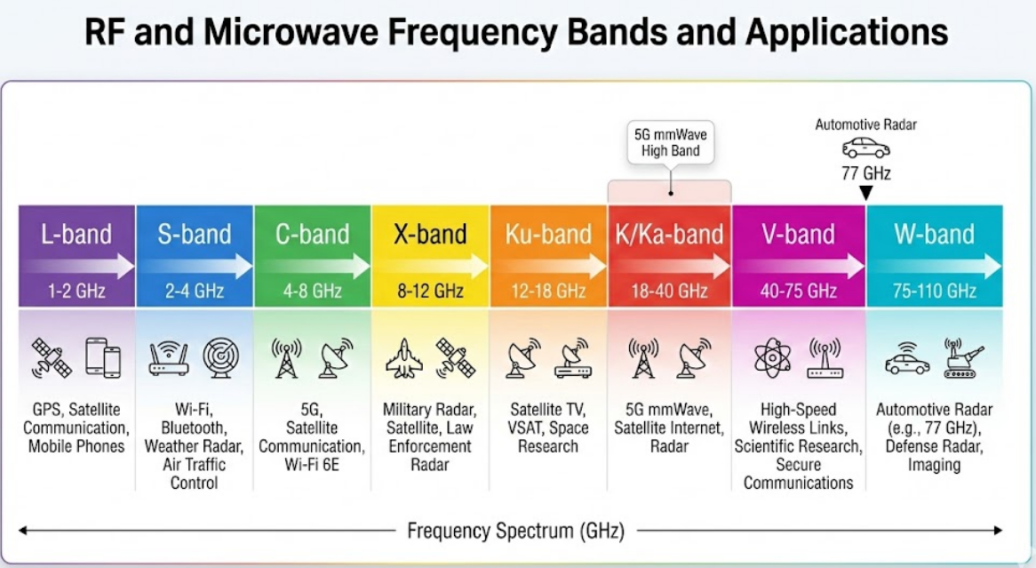
Radar systems and military electronic warfare extend to over 100GHz. Wi-Fi 6E and 7 have also been adopted even in consumer Wi-Fi. It is the explosive nature of all of these aspects that has necessitated a massive requirement for RF microwave PCBs that can easily and reliably operate at such high frequencies without signal degradation. Any loss of 0.1dB counts when you want to extract the last bit of range out of a 5G base station or achieve the best sensitivity with a radar receiver.
Challenges: Insertion Loss, Crosstalk, and Thermal Management
The art of designing a PCB for microwave is essentially a balancing act between three large issues that just keep on escalating as the frequency increases. First up, insertion loss. Each time the signal goes through a trace, via or through any interconnection, it is losing power, and at the gigahertz frequencies, loss actually compounds very rapidly. A 77 GHz automotive radar signal can lose 2-3 dB per centimeter in a poorly designed transmission line, which makes every millimeter of trace length a precious resource.
Next is crosstalk. In the case of proximity between two transmission lines, the fields begin to interfere. At 28 GHz, two parallel microstrip lines spaced at three times the dielectric thickness can still exhibit -20 dB or worse coupling. And it is enough to corrupt a sensitive receiver input.
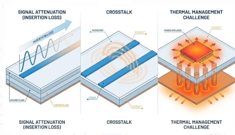
And lastly, there is the matter of thermal management. A high level of heat is generated by power amplifiers, mixers, and oscillators, and their performance metrics, which include gain, noise figure, and linearity, change significantly with temperature. The PCB must be able to effectively extract that heat and maintain the precise impedance environment that high-frequency signals require.
Specialized Materials Driving RF Microwave Performance
Low-Dk/Df Laminates Such as Rogers and PTFE-Based Options
Material selection is arguably the most consequential decision in RF microwave PCB design. The substrate’s dielectric constant (Dk) and dissipation factor (Df) directly determine transmission line dimensions and signal loss.
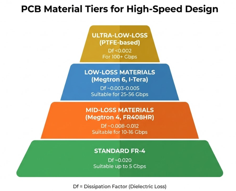
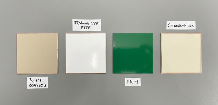
Rogers Corporation dominates the RF laminate market with products spanning a wide performance range. RO4003C and RO4350B offer excellent performance to about 20 GHz with good processability. RO3003 and RO3010 extend into millimeter-wave territory with very low Df values. RT/duroid 5880, a PTFE-glass laminate with Df around 0.0009 at 10 GHz, is the gold standard for the lowest-loss applications.
According to what I have studied during our recent modules, PTFE laminates based on PTFE demonstrate outstanding electrical characteristics, but present a number of manufacturing challenges: they have low peel strength to copper, require special drilling to avoid smearing, and cannot bond with standard FR-4 in hybrid stack-ups without adhesive layers. These trade-offs are important to understand to make knowledgeable choices of materials.
Copper Foil Quality and Surface Roughness Impact
In microwave frequencies, the skin effect restricts the current flowing to a nearly unattainable layer of conductor. The skin depth of copper at 10 GHz is approximately 0.66µm, and therefore any surface roughness, which is usually 1 to 5 µm in standard electrodeposited foils, makes the current take a longer and more winding path, thereby increasing conductor loss.
Low-profile and ultra-low-profile copper foils (such as rolled annealed or hyper-VLP foils) reduce surface roughness to below 1µm, providing measurable loss reduction at frequencies above 5 GHz. The improvement can be 0.5-1.5 dB per inch at 28 GHz, which is substantial for any microwave design. Specify the copper foil type in your fabrication notes. Standard ED foil is adequate below about 5 GHz, but above that, the investment in low-roughness foil pays for itself in improved system performance.
Pro-Tip: When comparing laminate datasheets, pay attention to the copper foil used for the published loss data. Some manufacturers test with ultra-smooth foil, making their laminate look better than it will perform with the standard foil your fabricator stocks. Always specify your foil requirement explicitly.
Hybrid Material Stacks for Balanced Cost and Performance
High-quality PTFE or even high-quality ceramic-filled stackups are costly, and not all RF designs require such high-quality materials on all layers. To achieve a cost-effective solution, hybrid stackups are used, where the RF signal-carrying laminates are made of low-loss material, and the power-distribution and low-speed digital carrying layers are made of inexpensive FR-4 or mid-range materials. An RF front-end module may have a standard FR-4 core with Rogers RO4350B on the top two layers (where the microstrip and stripline circuits are located) and standard FR-4 on the core with power and ground, and perhaps a second RF signal, in which case you could also use another Rogers layer.
Prepreg layers of adhesive hold the various materials together, and the Dk of these layers is adjusted to ensure that the impedance remains relatively constant. This has the potential to reduce the price of laminate by approximately 40 to 60% and retain full RF performance on the critical layers. The point is that it is necessary to ensure that the adhesive layers and the boundaries between materials do not produce impedance jumps and delamination.
Core Engineering Principles for RF Microwave PCBs
Impedance Matching, Transmission Line Design, and Grounding Techniques
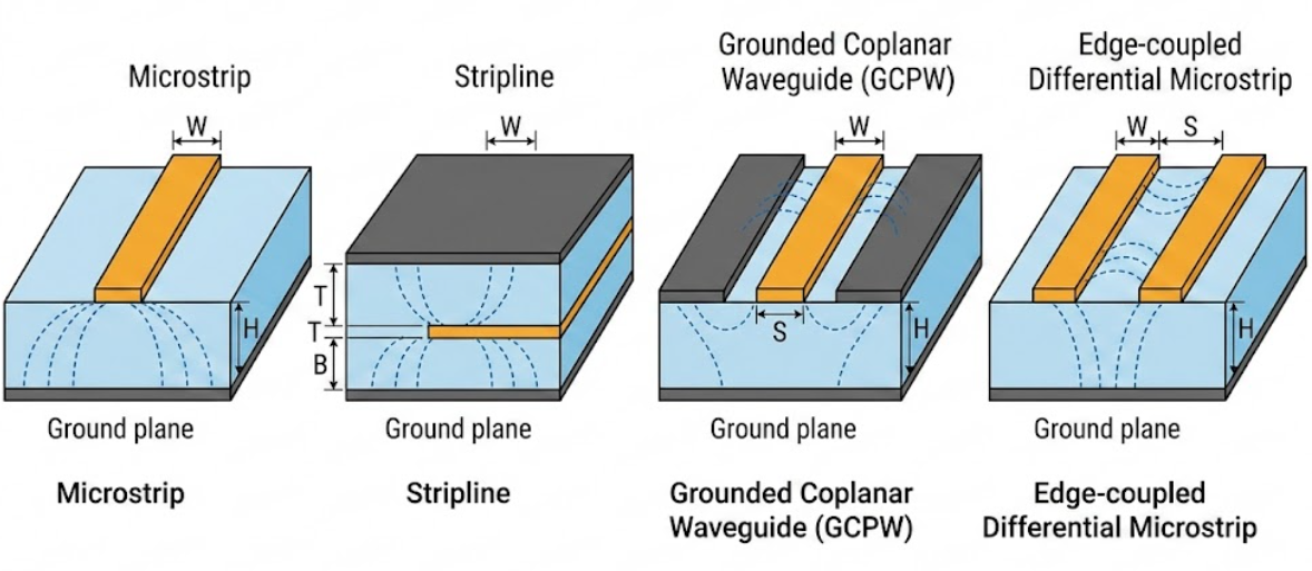
All RF traces on a microwave PCB are simply transmission lines, meaning that you must control their impedance very tightly. Microstrip, with the trace on the surface, and stripline with the trace between two ground planes are the common suspects. Next, there is the grounded coplanar waveguide (GCPW), which is a surface trace surrounded by ground copper on the same sheet and is still covered by a ground plane under it; it is a bit more flexible and has better isolation.
In matching impedance at all junctions: pad edges, via drops, and connector starts, you want a return loss of at least -15 dB, but since even the most demanding applications require it, -20 dB or better. You will find people use quarter-wave transformers, tapered transitions, or matching networks to maintain the impedance constant all the way through.
Grounding is the foundation of microwave PCB performance. A solid, continuous ground plane immediately adjacent to every RF signal layer is non-negotiable. Via stitching along RF transmission lines controls the ground plane’s resonant behavior and prevents unwanted mode propagation between parallel plates.
Via Optimization and Shielding for Noise Reduction
Vias in RF circuits must be treated as designed elements, not routing conveniences. Each via introduces parasitic inductance (typically 0.5-1.5 nH depending on geometry) and capacitance that create impedance discontinuities. Multiple parallel ground vias around signal vias reduce the effective inductance and create a coaxial-like transition.
For critical signal transitions, use via arrays or via fences to create shielded passages through the board. An RF microwave isolator effect can be achieved by surrounding sensitive signal paths with dense via fences connected to ground planes above and below, creating in-board waveguide structures that contain electromagnetic energy.
Shielding between channels is essential in multi-channel systems. Via fences between adjacent RF channels provide 20-40 dB of isolation depending on via pitch and frequency. For higher isolation requirements, internal metal walls (created with overlapping via rows) or board-level shielding cans are necessary.
Thermal and Mechanical Considerations in Layout
Power amplifiers and active RF components generate concentrated heat that must be managed to maintain performance and reliability. Thermal via arrays under hot components, connecting to internal or external copper spreaders, are the primary thermal management tool at the PCB level.
Mechanical considerations include CTE (coefficient of thermal expansion) matching between dissimilar materials in hybrid stackups, board warpage during reflow (particularly for thin PTFE-based boards), and structural integrity of the via-to-pad connections under thermal cycling. These factors influence both the laminate selection and the physical layout of the RF circuit.
Expert Fabrication Techniques Ensuring RF Microwave Reliability
Tight Tolerance Etching, Drilling, and Plating Processes
RF microwave PCB fabrication tolerances are significantly tighter than standard boards. Trace width tolerance of ±0.5 mil or better is typical for controlled-impedance RF lines. Etch profile control — the cross-sectional shape of the etched trace — is critical because trapezoidal profiles (inevitable with wet etching) change the effective impedance compared to the ideal rectangular profile assumed by most impedance calculators.
Drilling PTFE-based laminates requires specialized bit geometry and feed rates to prevent resin smearing that can degrade reliability. Plating adhesion to PTFE surfaces requires surface treatment (sodium etching or plasma treatment) that is not needed for standard FR-4.
Controlled Lamination and Surface Finish Application
Laminating hybrid stackups with dissimilar materials demands precise temperature and pressure control. The bonding adhesive must flow adequately to fill gaps around copper features while maintaining controlled thickness for impedance accuracy. Under-fill creates voids; over-flow changes dielectric thickness.
Surface finish choice for RF pads favors immersion silver or ENIG, both of which provide flat surfaces for consistent component attachment. For gold wire bonding (common in RF module assembly), electrolytic nickel-gold (hard gold) or soft gold finishes are required. The surface finish must be specified for each pad area individually when different requirements exist on the same board.
Rigorous Testing for S-Parameters and Signal Integrity
Comprehensive testing distinguishes a professional RF microwave fabrication facility from a general-purpose shop. TDR impedance measurements verify transmission line impedance across the panel. Vector Network Analyzer (VNA) measurements on dedicated test structures characterize insertion loss, return loss, and coupling (S-parameters) at the actual operating frequencies.
These test results provide objective proof of fabrication quality and serve as baseline data for correlating PCB performance with system-level measurements. A high-quality RF PCB manufacturer provides this data routinely as part of the quality package.
JLCPCB’s Leadership in RF Microwave PCB Production
Access to Premium Materials and Advanced Manufacturing Lines
The material portfolio of JLCPCB is a fairly strong one; they have the Rogers, PTF-based, and ceramic-filled laminates, which are slick when it comes to RF components between UHF and millimeter-wave. Combine that with their high-precision machining equipment capable of striking the tight tolerances such as those required by the microwave circuit, and you have a high-quality RF microwave PCB production service, basically.
Customized DFM Guidance for Optimal High-Frequency Outcomes
When you have the fab guys on your design early on, doing HF RF designs is much easier. The JLCPCB engineering group would be happy to discuss the material choices, tolerances you can really achieve, stacking up hybrids, and the best surface finish in your particular RF project. That early collaboration prevents you from having to redesign your design again later and ensures that your design is actually manufacturable.
Scalable Solutions from Prototypes to Volume Manufacturing

JLCPCB maintains the same process quality of RF microwave boards through the first prototype tests, to the last production run. Their material options, production processes, and quality checks remain the same irrespective of size, hence your prototype will translate to the end product. Simply add your RF design files, and then the automatic DFM checker will ensure that your board is ready to be manufactured.

Frequently Asked Questions (FAQ)
Q. What is the difference between RF and microwave PCBs?
The terms are often used interchangeably in the PCB industry. Strictly, RF covers the broad 3 kHz to 300 GHz range, while microwave specifically refers to 300 MHz to 300 GHz. In practice, an RF microwave PCB describes any board designed for signals above approximately 500 MHz.
Q. Can standard FR-4 be used for RF applications?
FR-4 can work for less demanding RF applications below about 1-2 GHz, where moderate loss is acceptable. Above 2 GHz, the dielectric loss of FR-4 degrades signal quality significantly.
Q. How does copper roughness affect RF performance?
Copper surface roughness increases conductor loss at microwave frequencies due to the skin effect, which confines current flow to the conductor surface. At 10+ GHz, switching from standard electrodeposited foil to ultra-low-profile foil can reduce insertion loss by 0.5-1.5 dB per inch.
Q. What impedance tolerance should I specify for RF traces?
Standard controlled-impedance tolerance is ±10%. For demanding RF applications, specify ±7% or ±5%. Tighter tolerances require premium fabrication processes and may increase cost.
Q. Why are hybrid stackups popular for RF boards?
Hybrid stackups use premium low-loss laminates only on the layers carrying RF signals and cost-effective FR-4 on non-critical layers. This reduces material cost by 40-60% while maintaining full RF performance where it matters.
Keep Learning
Building Reliable High-Speed Performance with Effective Timing Analysis
Key Takeaways Timing analysis is essential for high-speed PCBs — clean signals can still fail if they miss setup or hold windows. Focus on setup time, hold time, clock skew, and propagation delay to ensure reliable data sampling. Prioritize length matching, controlled impedance, and proper stackup to maintain positive timing margins. Combine static timing analysis with dynamic simulation for best results. Precision manufacturing is critical — small variations in impedance or dielectric thickness can d......
Low Loss PCBs : Advanced Materials for Superior High-Speed Signal Performance
Key Takeaways Low Loss PCBs using advanced materials like Rogers RO4003C, RO4350B, and PTFE laminates deliver superior signal integrity by dramatically reducing dielectric loss at multi-gigahertz frequencies. Ideal for 5G, mmWave, RF, and high-speed digital designs, these boards offer significantly lower insertion loss, stable impedance, and better thermal performance compared to standard FR4. By choosing the right low-loss laminate and partnering with experienced manufacturers like JLCPCB, engineers ......
How to Reduce Insertion Loss for Better High-Speed PCB Performance
Key Takeaways Reducing insertion loss is essential for achieving reliable high-speed PCB performance. By selecting low-loss materials with lower Df, optimizing trace routing and stackup design, minimizing via transitions, using smoother copper foils, and applying precision manufacturing techniques, designers can significantly lower both dielectric and conductor losses. These strategies help maintain better signal integrity, wider eye openings, and higher data rates in multi-gigabit designs. Have you e......
How to Create the Perfect PCB Stackup for High-Speed and Reliable Designs
Key Takeaways A well-designed PCB stackup is the foundation of high-speed, reliable designs, determining signal integrity, controlled impedance, and EMI performance. Use symmetrical layers with adjacent reference planes, proper dielectric spacing, and copper balancing to avoid warpage and crosstalk. Choose standard FR4 for <3 GHz or low-loss materials (Megtron 6, Rogers) for higher speeds, and work closely with manufacturers for optimal results. Mastering your stackup is essential for high-speed succe......
Achieving Reliable High-Speed Performance with PCB Transmission Lines
Key Takeaways PCB Transmission Lines are essential for reliable high-speed PCB performance in USB 3.0, PCIe, DDR4, and RF designs, turning traces into controlled-impedance structures that eliminate reflections, crosstalk, and attenuation. Select microstrip, stripline, or GCPW geometries with accurate calculations, continuous reference planes, mitered bends, and 3W spacing, then rely on precise etching, copper profile control, and TDR testing at JLCPCB for consistent results from prototype to volume pr......
Backdrill Vias: Enhancing Signal Integrity in High-Speed PCBs
Key Takeaways Backdrill vias remove unused copper stubs from plated through-hole vias, shortening the residual stub to under 0.15 mm (6 mils). This eliminates impedance discontinuities, reflections, and resonances in high-speed signals above 5–10 Gbps. It delivers better return loss, insertion loss, lower jitter, and clearer eye diagrams — all while keeping simple stack-ups and far lower cost than blind/buried vias. Use backdrilling for any stub longer than 15 mils (0.381 mm), especially on boards thi......