DDR5 PCB Layout Guidelines: Design Rules and Best Practices
14 min
- Introduction
- DDR5 Architecture and PCB Impact
- Stackup and Material Selection
- Layout Guidelines and Best Practices
- Power Delivery Network Design
- Signal Integrity Verification
- Common Mistakes about DDR5 PCB Design
- DDR5 PCB Design Checklist
- FAQ about DDR5 PCB Layout
- Conclusion about DDR5 PCB Layout
Key Takeaways
- DDR5 raises the stakes on layout: 1.1V rails and data rates up to 8800 MT/s leave far less margin for error than DDR4 did.
- Target around 40–45 Ω single-ended for DQ/CA and 80 Ω differential for CLK/DQS — exact values come from vendor guidelines — and hold them through every via and connector.
- Keep DQ and DQS length matching within about 5 mil per byte lane, and never route a DDR5 signal over a gap in its reference plane.
- Plan for 8 to 12 layers with dedicated ground references next to every signal layer, not after routing is already underway.
- The on-DIMM PMIC shifts power integrity work onto the module, but the host board's PDN still needs its own impedance budget.
Introduction
A DDR5 design passes simulation, then fails intermittently once it ships. Nothing on the schematic looks wrong. The parts are the right ones, the pinout matches the datasheet, and the board still won’t hold a stable link at full speed.
This is usually a layout problem, not a component problem. DDR5 raised the data rate to 6400 MT/s at its original JEDEC release, and the spec has since been extended to 8800 MT/s. (JEDEC, JEDEC Updates JESD79-5C DDR5 SDRAM Standard) At the same time, the core voltage dropped from DDR4’s 1.2V to 1.1V. Faster edges and a smaller voltage swing add up to noise margins that used to forgive a sloppy trace and no longer do.
DDR5 also changed where some of the hard problems live. Voltage regulation moved off the motherboard and onto the DIMM itself, DQ lines gained decision feedback equalization to fight channel loss, and the pinout shifted enough that a DDR4 breakout strategy doesn’t just carry over.
This article walks through the DDR5 PCB layout guidelines that matter in practice: stackup and material selection, routing and length matching, power delivery, and signal integrity verification. Each section sticks to numbers and rules you can apply directly, not general theory you already know. The focus here is conventional DDR5 SDRAM interfaces in DIMM and memory-down designs; exact constraints vary by controller, memory topology, and vendor, so treat the numbers as starting points and defer to your vendor’s guidelines where they differ.
DDR5 Architecture and PCB Impact
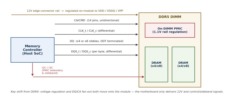
Figure 1. DDR5 moves voltage regulation onto the DIMM. The motherboard delivers a 12V rail plus control, clock, and data groups.
DDR5 vs DDR4
| DDR4 | DDR5 | |
|---|---|---|
| Standard max data rate | 3200 MT/s | 6400 MT/s (to 8800 MT/s) |
| Core / I/O voltage | 1.2V | 1.1V |
| Voltage regulation | Motherboard VRM | On-DIMM PMIC |
| Channel structure | One 64-bit channel | Two independent 40-bit sub-channels (32 data + 8 ECC) |
| Command/address bus | Wide parallel CA | Per-sub-channel CA bus, fly-by topology |
Voltage regulation moving to an on-module PMIC shifts the host board’s job from "deliver 1.2V cleanly" to "deliver a clean 12V rail." DDR5 also splits each DIMM into two independent 32-bit (plus ECC) sub-channels instead of one 64-bit channel, reshaping how CA, CLK, and DQ groups fan out from the controller.
Sub-Channel Topology and CA Fan-Out
DDR5 divides each DIMM into two independent 40-bit sub-channels (32-bit data plus 8-bit ECC on ECC modules), and this reorganizes how signals leave the controller. Each sub-channel carries its own CA bus, CLK pair, and DQ/DQS groups, so what used to be one wide 64-bit channel becomes two narrower, self-contained sets of routing rules.
The topology within each sub-channel, however, is closer to DDR4 than it first appears. On DIMM-based designs, CLK and CA/CMD still fly by the DRAMs in series — the chains are simply shorter, with fewer devices per chain — while DQ and DQS run point-to-point to a single device, as they did in DDR4. Board-level topology ultimately depends on the memory configuration: memory-down designs can shorten the CA chain considerably. Plan the breakout so each sub-channel’s CA, CLK, and DQS groups fan out without crossing the other sub-channel’s escape paths, and route each sub-channel as a parallel copy of the same rule set.
DDR5 Pin Layout Essentials
The DDR5 pin layout groups pins by function: DQ bytes, DQS strobe pairs, the CA/CMD bus, and the differential CLK_t/CLK_c. Each group has its own impedance and length-matching rules, so keep them visually separated in schematic and layout.
Host-side BGA ball pitch is typically 0.65-0.8 mm, so breakout routing dominates the first few layers. Plan via patterns and layer assignment for fanout before placing a single trace, and set up differential-pair rules for CLK and DQS from the start.
Stackup and Material Selection
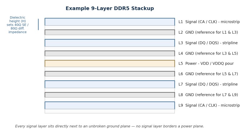
Figure 2. An example 9-layer DDR5 stackup keeps every signal layer next to a ground reference, with power isolated between two ground layers.
Choosing layer count, dielectric material, and target impedance together, rather than one at a time, keeps the stackup buildable and the signals clean. See our PCB stackup best practices guide for the general theory behind layer ordering.
Layer Count
A small single-rank interface can sometimes route on 8 layers. Many DDR5 motherboard and SoM designs land on 10-12 layers
Dual-rank designs or multiple DDR5 channels push toward 12 layers. If DQ groups end up crossing CA traces or sharing a plane with power, that is the signal to add a layer rather than force the routing through.
Dielectric Material
Conventional FR-4 laminates have loss tangents typically around 0.015–0.02, varying by resin system and glass style — fine at low speed, but a real contributor to eye closure on longer traces at 6400 MT/s and above. Low-loss laminates such as Megtron 6, FR408HR, or I-Speed bring that down to roughly 0.004-0.01. (Isola, FR408HR Laminate and Prepreg)
Glass weave also matters: standard weave creates periodic dielectric-constant variation that shows up as skew between traces in a differential pair. Spread-glass or rotated-weave laminates reduce this, worth the cost on tight DQS or CLK pairs.
Impedance Targets
DQ and CA single-ended signals typically target ~40 Ω — some controller design guides, such as Intel’s, list 45 Ω for specific stripline configurations — and CLK/DQS differential pairs target ~80 Ω. (Intel, DDR5 PCB Layout Guidelines) Always confirm exact values against your controller and DRAM vendor’s design guidelines.
| Signal Group | Type | Target Impedance |
|---|---|---|
| DQ (data) | Single-ended | ~40 Ω |
| CA/CMD (address/command) | Single-ended | ~40 Ω |
| DQS (data strobe) | Differential | ~80 Ω |
| CLK_t / CLK_c | Differential | ~80 Ω |
Impedance must hold through the entire channel, not just straight trace sections. Vias, connector footprints, and reference-plane transitions are the usual discontinuity points, and DDR5’s tight margins make each reflection cost more.
Calculate trace geometry against your real stackup with a 2D field solver or an online impedance calculator, using actual copper weight and dielectric constant. Budget roughly ±10% tolerance as a starting target.
Layout Guidelines and Best Practices
This is the section to keep open while you’re actually routing. The rules below cover placement, trace routing, vias, reference planes, crosstalk, and decoupling, the decisions that determine whether the board works on the first spin.
Component Placement
Keep the DRAM close enough to the controller for short, matchable traces, but leave room for decoupling caps and via fanout. Orient the package so DQ/DQS pins face the controller directly whenever the pinout allows it.
Thermal matters more here than on DDR4 because the on-DIMM PMIC and denser routing both add heat. Keep decoupling caps close to their power pins without blocking escape routing for nearby signals.
Trace Routing and Length Matching
Match DQ to DQS within about 5 mil per byte lane as a typical starting point — the final constraint is the skew or propagation-delay budget in your controller vendor’s guidelines, not a universal mil value. Across byte lanes, the allowable skew should likewise follow the controller's training and timing budget rather than a fixed PCB length tolerance. Keep CLK_t/CLK_c intra-pair skew similarly tight, since skew there adds jitter to every signal using that clock.
Use serpentine routing to close small gaps, but keep amplitude conservative — space bumps at least 3× the trace width apart. Keep controller-to-DIMM traces short; every added inch eats into the insertion-loss budget.
Via Design
Every via is a small impedance discontinuity and potential resonant stub. Keep DQ, DQS, and CLK on a single layer where routing density allows, and treat any unavoidable layer change carefully.
Back-drill unavoidable vias to remove unused stub, or use blind/buried microvias on simpler boards. Place a ground via close to any signal via that changes layers — within about 20-30 mil is a common starting point — so return current has a short path; the exact spacing depends on your stackup and via geometry.
Reference Planes and Crosstalk
An unbroken reference plane keeps return current tracking directly under the signal, which is what holds impedance steady. A split, slot, or keepout crossing under a DDR5 trace forces a detour that can measurably close the eye.
Vendor-recommended or 3H spacing, where H is the distance from the trace to its reference plane, is the more rigorous crosstalk constraint for tight DDR5 routing; the familiar 3W rule — spacing at least 3× the trace width — works as an early guideline but should not replace stackup-based crosstalk analysis. Watch especially where CLK or DQS runs parallel to a DQ byte group, since crosstalk into the timing reference adds jitter even if DQ looks clean.
Decoupling Capacitors
Use a layered approach: bulk capacitance (tens to hundreds of µF) for low-frequency transients, mid-range (0.1-1 µF) for the mid-band, and high-frequency (1-10 nF or smaller) placed as close to power pins as possible.
Via-in-pad construction helps place high-frequency caps with the shortest loop to ground. Keep them as close as practical to the pins they decouple — within roughly 100 mil is a common starting point — and let the DRAM or PMIC vendor’s reference design, rather than a fixed recipe, drive the final capacitor selection and placement.
Power Delivery Network Design
DDR5 shifted a large share of power integrity work onto the module by putting a PMIC on the DIMM itself. That doesn’t remove the host board’s responsibility — it changes what the host board’s PDN needs to deliver.
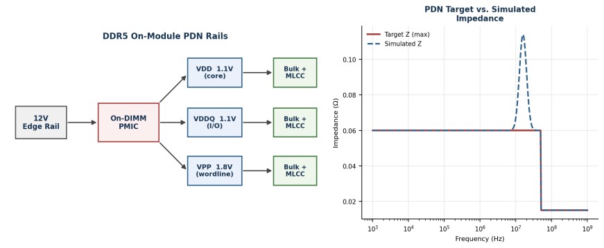
Figure 3. The on-DIMM PMIC regulates 12V down to VDD, VDDQ, and VPP (left); the simulated PDN impedance is checked against its target profile (right).
Allocate sufficient copper area and low-inductance paths for each major rail (VDD, VDDQ, 12V input) rather than splitting one plane into isolated pours, which avoids copper slivers and via-placement risk; whether a rail needs its own dedicated plane depends on the stackup, current demand, and PDN analysis. Keep pour continuous under the DDR5 IC footprint, and skip thermal reliefs on power vias.
Target impedance starts with allowed voltage ripple divided by worst-case transient current. Simulate the PDN with real capacitor values and plane geometry before finalizing placement — resonant peaks usually show up at the crossover frequency between capacitor tiers.
Signal Integrity Verification
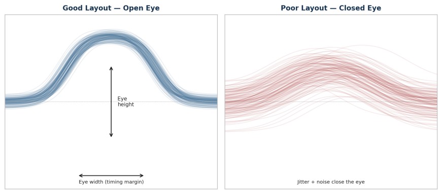
Figure 4. An open eye reflects controlled impedance, tight length matching, and clean reference planes.
An eye diagram overlays many bit periods on top of each other. Eye height reflects voltage margin; eye width reflects timing margin. Where the interface uses DFE, it cancels some inter-symbol interference, but it only buys reserve margin
DDR5 relies mainly on on-die termination rather than external resistors, which puts more weight on getting layout impedance right in the first place. After routing, extract S-parameters from the actual layout and run an IBIS-based simulation to generate a real eye diagram, then check it against the compliance mask with margin to spare.
Common Mistakes about DDR5 PCB Design
Common Mistakes
- Reusing a DDR4 stackup and routing strategy. DDR5’s tighter margins don’t forgive DDR4-era impedance tolerances or length-matching windows.
- Treating the on-DIMM PMIC as someone else’s problem. The 12V rail still needs its own decoupling and a clean path to the connector.
- Under-matching CA/CLK length while over-matching DQ. CLK times everything else on the bus, so skew there outweighs tight DQ matching.
- Routing across a connector shield keepout or mounting-hole cluster. Check reference-plane continuity at every board edge, connector, and mechanical keepout.
DDR5 PCB Design Checklist
- Layer count matches channel count and bus width, typically 8 to 12 layers, with a dedicated ground reference next to every signal layer.
- Dielectric material loss tangent and glass weave selected for your target data rate, not defaulted to standard FR-4.
- Single-ended (typically ~40–45 Ω) and differential (~80 Ω) impedance targets confirmed against vendor guidelines and your actual stackup with a field solver.
- DQ-to-DQS and CLK intra-pair skew within the controller vendor’s timing budget (often only a few mils of trace length); byte-lane-to-byte-lane skew within the leveling range.
- No DDR5 signal routed across a plane split, connector keepout, or mounting-hole cluster.
- Every via carrying a DDR5 signal paired with an adjacent ground via; unused stubs back-drilled or avoided with blind/buried vias.
- DDR5 signal groups spaced at least 3W apart, with extra spacing or guard traces where CLK/DQS runs parallel to DQ.
- Decoupling capacitors placed by tier, high-frequency closest to the pin, with via-in-pad used where the layout allows it.
- PDN target impedance calculated and simulated against actual capacitor placement before the board is finalized.
- Post-layout S-parameter extraction and IBIS-based eye simulation completed, with margin against the compliance mask, not just a pass.
FAQ about DDR5 PCB Layout
Q: What is the minimum number of PCB layers required for a DDR5 design?
Eight layers can work for a small, single-rank interface, but most designs that follow practical DDR5 PCB layout guidelines land on 10 to 12 layers once every signal layer needs its own ground reference and power gets a dedicated plane.
Q: How does DDR5 pin layout affect PCB routing complexity?
DDR5’s tighter ball pitch and dual sub-channel structure concentrate a large number of signals in a small breakout area, which pushes more routing complexity into the first few layers near the package and makes early fanout planning more important than it was for DDR4.
Q: What impedance values should I target for DDR5 single-ended and differential signals?
Roughly 40 Ω single-ended for DQ and CA, and roughly 80 Ω differential for CLK and DQS, though you should confirm exact values against your DRAM and controller datasheets since ODT settings vary by vendor and speed grade.
Q: Can I use standard FR4 material for DDR5 PCB design?
Standard FR-4 can work for shorter, lower-speed DDR5 channels, but its higher loss tangent starts costing real margin on longer traces or designs targeting the upper end of DDR5’s extended speed grades, where a low-loss laminate becomes worth the added cost.
Q: How do I verify my DDR5 layout meets signal integrity requirements?
Extract S-parameters from the actual routed layout, run an IBIS-based eye simulation using your vendor’s models, and compare the resulting eye diagram against the compliance mask with margin to spare. Vendor DDR5 reference design documentation typically budgets extra margin, because a layout that only barely passes simulation often fails once manufacturing variation is added.
Conclusion about DDR5 PCB Layout
Successful DDR5 PCB layout comes down to treating stackup, impedance, routing, power integrity, and signal integrity verification as one connected problem rather than four separate checklists. A stackup that doesn’t support your impedance target undermines careful routing. Routing that ignores the PDN’s needs undermines careful power planning. Each piece depends on the others.
Following these DDR5 PCB layout guidelines from the start of a design, not as a fix after the first prototype fails, is what prevents a costly re-spin. The rules here aren’t exotic: hold impedance, match lengths where it matters, keep reference planes unbroken, and verify with simulation before the board goes to fabrication.
If you’re working on a DDR5 design and want a second set of eyes on your stackup, routing, or impedance before you send it off, JLCPCB’s PCB layout service can review the design while it’s still easy to fix.
Keep Learning
SFP Pinout Explained: PCB Layout & Design Guide
Key Takeaways The SFP pinout follows a standard 20-pin edge connector, with dedicated pins for power, ground, differential data pairs, and I2C control signals. The Tx and Rx differential pairs carry the high-speed optical or copper signal and need controlled 100 ohm differential impedance through the entire routing path. Low-speed control pins (TX_FAULT, TX_DISABLE, MOD_ABS, LOS, Rate Select/RS1) use standard single-ended routing and don't need impedance matching. Placing the SFP cage near the board e......
DDR5 PCB Layout Guidelines: Design Rules and Best Practices
Key Takeaways DDR5 raises the stakes on layout: 1.1V rails and data rates up to 8800 MT/s leave far less margin for error than DDR4 did. Target around 40–45 Ω single-ended for DQ/CA and 80 Ω differential for CLK/DQS — exact values come from vendor guidelines — and hold them through every via and connector. Keep DQ and DQS length matching within about 5 mil per byte lane, and never route a DDR5 signal over a gap in its reference plane. Plan for 8 to 12 layers with dedicated ground references next to ev......
Via Stitching in PCB Design: A Complete Guide
Key Takeaways Via stitching bonds same-net copper across layers with repeated plated vias, most often ground, to cut high-frequency impedance between regions. A grounded via next to a signal layer transition gives return current a short local path and helps confine the field around the via. Via fences along board edges and RF cavities suppress edge radiation, but their isolation is geometry- and frequency-dependent, with no universal dB value. Keep stitching pitch at or below one-twentieth of the in-b......
Crosstalk in PCB Design: Causes, Types, and How to Reduce It
Key Takeaways Crosstalk starts at an edge: a changing aggressor voltage and current produce electric and magnetic fields that couple energy into a neighboring victim trace. Edge rate matters more than clock frequency alone. A modest-rate bus with fast I/O edges can still create a serious coupling problem. More spacing and a smaller signal-to-reference-plane distance usually provide the cleanest layout improvements, but the result depends on the complete cross-section. NEXT and FEXT do not scale in the......
Mastering IC Board Design: Layout Rules & Best Practices
Key Takeaways Placement is the foundation of good layout. Position ICs, decoupling capacitors, and crystals to minimize trace lengths before routing anything — placement quality determines most of your signal performance. Respect the physics, not just the schematic. High-speed designs demand controlled impedance (e.g., 90-ohm USB differential pairs), length matching, and a well-planned layer stackup to prevent reflections, crosstalk, and power noise. Handle power and heat deliberately. Size power trac......
LVDS PCB Layout Guidelines: Design Tips and Worked Example
Key Takeaways 100 Ω Differential Impedance: LVDS PCB layout starts with one number: 100 Ω of differential impedance. Trace width, spacing, and board thickness all set that number. Route Pairs Together: Route the two traces of a pair together, side by side, and keep their lengths within 5 to 10 mil of each other. Solid Ground Plane: Never let an LVDS pair cross a gap in the ground plane. It breaks the return path and hurts the signal. 4-Layer Minimum: A 4-layer board with a solid ground plane is enough......