
Transistor Pin Identification Using a Multimeter: Complete Step-by-Step Guide
14 min
- Understanding Transistor Pins Before Testing
- Tool Needed for Transistor Pin Identification
- Transistor Pin Identification Using a Multimeter [Step-by-Step Guide]
- Common Transistor Pin Identification Mistakes
- Checking a Transistor with a Multimeter: Troubleshooting Guide
- FAQs About Transistor Pin Identification
- Conclusion
Identifying transistor pins correctly is one of the first checks every engineer, hobbyist, and EE student needs before placing a bipolar junction transistor (BJT) into a circuit. A wrong base, collector, or emitter assignment can destroy the part on first power-up or leave a prototype board silently non-functional.
This guide explains how to identify transistor pins using a multimeter when no datasheet is available. The method works because a BJT is internally built from two PN junctions sharing a common base, the same structure found in a diode. That fact is what makes a multimeter's diode-test mode the right tool for the job.
By the end of this article, you will be able to:
- Find the base pin on an unmarked transistor
- Determine whether it is NPN or PNP
- Identify the collector and emitter
- Recognize the extra risk that SOT-23 and other SMD packages introduce
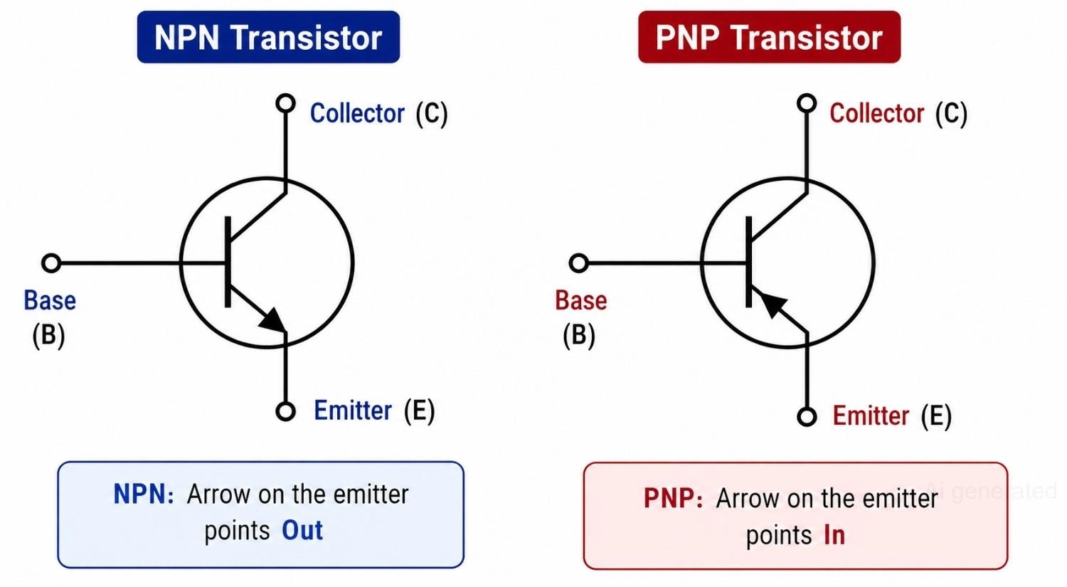
Figure: NPN and PNP transistor symbols showing base, collector, and emitter terminals.
Understanding Transistor Pins Before Testing
What Are the Base, Collector, and Emitter Pins?
A BJT has three terminals:
- Base (B): The control terminal. A small current here turns the transistor on and allows a much larger current to flow between the collector and the emitter.
- Collector (C): Carries the larger current into or out of the transistor, depending on the type.
- Emitter (E): The terminal current flows from (NPN) or into (PNP) on its way back to the supply.
Misidentifying any of these three terminals during manual assembly is one of the most common causes of "dead on arrival" prototype boards, even when every other component on the circuit is correct. When preparing designs for professional PCB Assembly, correct pin mapping is crucial to ensure that automated assembly machines place components with the correct orientation.
Why a BJT Behaves Like Two Diodes
Internally, a BJT is two PN junctions arranged back-to-back, sharing the base region:
- Base-Emitter junction
- Base-Collector junction
Because each junction behaves like an individual diode, a multimeter's diode-test mode can probe each junction independently. This physical structure is the foundation of every identification step that follows.
However, it is vital to know that this diode equivalence only works for testing purposes; you cannot build a functional transistor simply by wiring two separate diodes together, as the physical base region in a real BJT must be extremely thin to allow minority carrier diffusion.
If you are working with field-effect components instead, understanding the fundamental differences between a BJT vs MOSFET will help you avoid applying BJT diode-test logic to insulated gate terminals.
NPN vs PNP Transistor
NPN and PNP transistors differ in current carrier type, junction polarity, and the schematic arrow direction. These differences translate directly into how a multimeter probe responds to each pin.
| Feature | NPN | PNP |
|---|---|---|
| Current carriers | Electrons | Holes |
| Symbol arrow | Outward (on emitter) | Inward (on emitter) |
| Base polarity | Positive relative to the emitter | Negative relative to the emitter |
| Diode test direction | Red probe on base | Black probe on base |
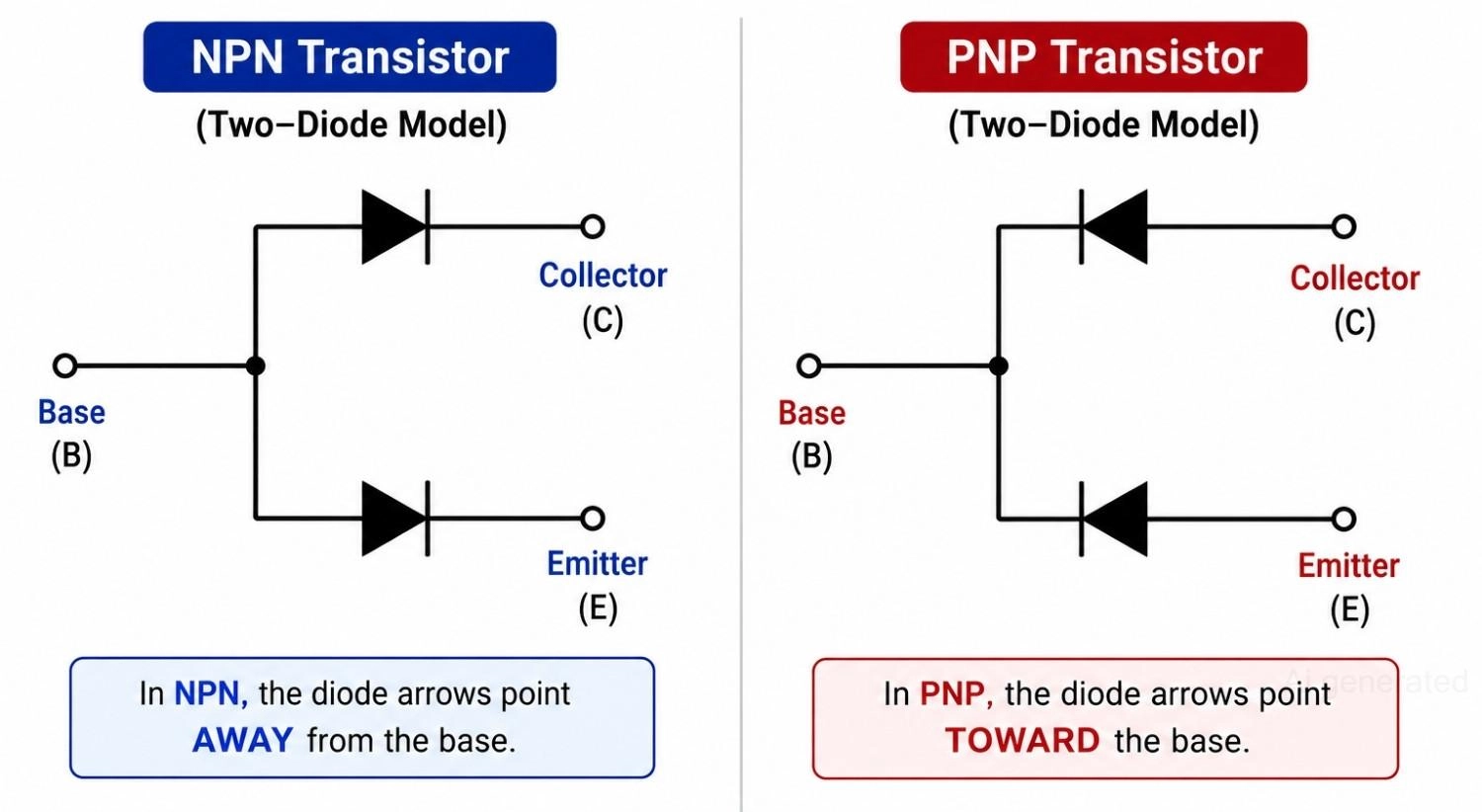
Figure: NPN and PNP transistors represented as two diode junctions sharing a common base.
Tool Needed for Transistor Pin Identification
Digital Multimeter with Diode Test Mode
A digital multimeter (DMM) with a dedicated diode test mode (marked with a diode symbol, an arrow pointing at a vertical line) is the primary tool required. This mode is vastly superior to resistance (ohms) mode. A standard resistance mode uses very low voltages to prevent turning on semiconductor junctions in-circuit.
Conversely, the diode test mode applies a small, constant current (typically around 1 mA) and measures the resulting forward voltage drop across the junction. This gives a clear, reliable voltage reading (in Volts) instead of an ambiguous, fluctuating resistance value.
Safety Tips Before Transistor Testing with Multimeter
Always remove the transistor from the circuit board before testing whenever possible.
Testing in-circuit risks parallel paths through other components, such as bias resistors, inductor windings, or capacitors, which can produce false voltage readings.
Measuring with the transistor still soldered in place is one of the most common sources of an incorrect result.
If testing confirms that a transistor has failed, replacing it with the correct part is the next step. Browse the JLCPCB Parts Library to source genuine BJTs and matching passive components from trusted manufacturers for your repair or next PCB project.
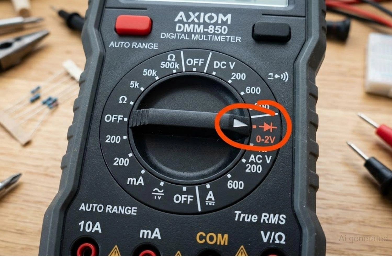
Figure: Multimeter rotary dial highlighting the diode test mode symbol.
Transistor Pin Identification Using a Multimeter [Step-by-Step Guide]
Step 1: Set the Multimeter to Diode Test Mode
Locate the diode symbol on your multimeter's rotary dial and turn the selector to that mode. In this mode, a healthy silicon PN junction produces a forward voltage reading between 0.55 V and 0.75 V. A reversed junction or an open circuit will show "OL" (Over Limit or Open Loop) on the display.
| Reading | Meaning |
|---|---|
| 0.55V - 0.75V | Good silicon junction (forward-biased) |
| 0.2V - 0.3V | Germanium junction (forward-biased) |
| OL | Open circuit or Reverse-biased junction |
| 0.00V | Shorted junction (Damaged semiconductor) |
Step 2: Find the Base Pin of the Transistor
Before testing, label the unknown leads as Pin 1, Pin 2, and Pin 3 with a marker or small sticky tab. Do not assume the pin order based solely on the package shape. Many through-hole packages that look identical can use completely different internal pin layouts.
To find the base, you must systematically test the combinations. The base is the only terminal that will produce a forward voltage drop (around 0.6 V for silicon) when paired with both of the other two pins using a specific probe polarity.
- Connect the Red (positive) probe to Pin 1. Touch the Black (negative) probe to Pin 2, then Pin 3. Record the readings.
- If both readings show a forward voltage drop (e.g., 0.6 V to 0.7 V), then Pin 1 is the Base, and the transistor is an NPN type.
- If not, move the Red probe to Pin 2 and repeat the test on Pin 1 and Pin 3.
- If that fails, move the Red probe to Pin 3 and test Pin 1 and Pin 2.
- If you still have not found a common anode, switch polarities: Connect the Black probe to Pin 1 and test with the Red probe on Pin 2, then Pin 3. If both conduct, Pin 1 is the Base, and the transistor is a PNP type.
- Repeat this process with the Black probe on Pin 2, then Pin 3, until you locate the common terminal that connects to both other pins.
| Red Probe (+) | Black Probe (-) | Reading | Conclusion |
|---|---|---|---|
| Pin 1 (Base) | Pin 2 | 0.62V | Forward junction found |
| Pin 1 (Base) | Pin 3 | 0.61V | Forward junction found |
| Pin 2 | Pin 3 | OL | No direct PN junction |
Example measurement walkthrough
In this set of readings, Pin 1 produced a forward voltage against both Pin 2 (0.62 V) and Pin 3 (0.61 V), while Pin 2 and Pin 3 showed no connection to each other (OL) in either direction. Because Pin 1 forms a junction with both remaining pins, Pin 1 is the base. Pin 2 and Pin 3 are the collector and emitter, in an order still to be determined in Step 4.
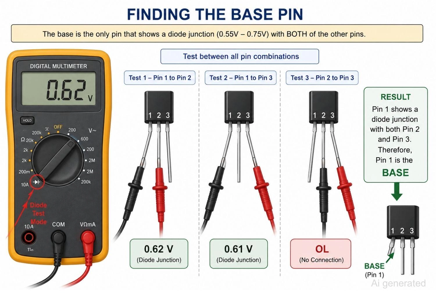
Figure: Multimeter probe placement on a transistor for base pin identification.
Step 3: Determine Whether the Transistor Is NPN or PNP
Once you have successfully identified the base pin, determining the polarity type (NPN or PNP) is incredibly simple based on which probe was held static on the base pin during conduction:
- How to identify NPN transistor: The Red (positive) probe is connected to the base pin, and the Black (negative) probe produces a forward voltage drop when touching the other two pins.
- How to identify PNP transistor: The Black (negative) probe is connected to the base pin, and the Red (positive) probe produces a forward voltage drop when touching the other two pins.
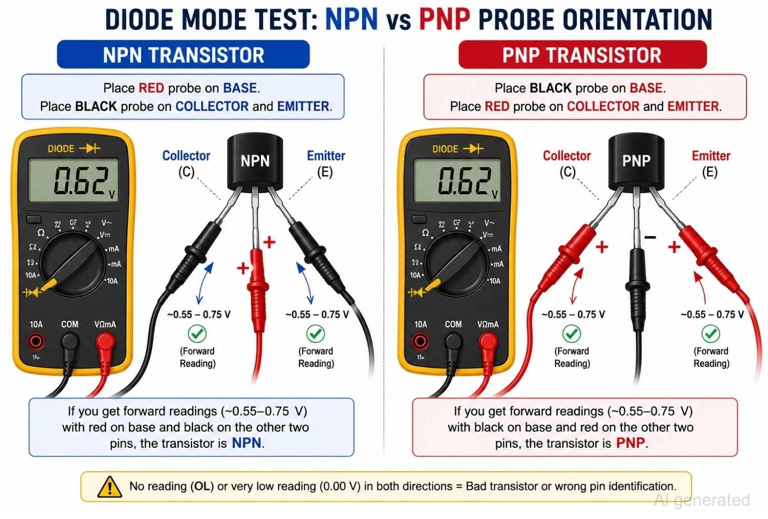
Figure: Multiple Probe Placement for NPN vs PNP
Step 4: Identify the Collector and Emitter Pins
This is the most technically challenging step.
The base-emitter (B-E) and base-collector (B-C) junctions read very close to each other. On many modern digital multimeters, the resolution might show only a tiny difference. Because of this, relying on simple diode-mode voltage alone can be an approximation rather than a guaranteed answer.
Note
Use one of the three following methods to confirm the pins with certainty.
Method 1: Compare Junction Voltage Drop (Approximate)
The physical properties of BJTs dictate that the emitter is typically more heavily doped than the collector to maximize carrier injection efficiency into the base. This heavier doping results in a slightly higher forward voltage drop across the base-emitter junction compared to the base-collector junction.
- Base-Emitter (B-E) junction voltage: Slightly higher drop (e.g., 0.635 V).
- Base-Collector (B-C) junction voltage: Slightly lower drop (e.g., 0.628 V).
Note: Since the difference can be as small as 1 mV to 5 mV, ensure your multimeter probes make clean, firm contact with the legs to avoid contact-resistance errors.
Method 2: Use hFE Mode (Preferred)
Most benchtop and handheld multimeters feature an "hFE mode" socket for measuring the DC current gain (beta) of a transistor.
- Insert the transistor leads into the NPN or PNP-designated slots on the meter's socket.
- Try both possible pin orientations for the remaining two leads (assuming you already know which one is the base).
- The orientation that yields a significantly higher hFE (gain) reading is correct. If you connect it backward (reversing the collector and emitter), the transistor operates in "reverse-active mode," which exhibits extremely poor current gain (typically less than 10, compared to a normal gain of 100 to 500).
Method 3: Build a Simple LED Test Circuit (Most Reliable)
If your multimeter lacks an hFE slot, you can verify the pins on a breadboard:
- Wire a current-limiting resistor (around 1 kΩ) from your VCC supply rail (e.g., 5 V) to the suspected collector pin.
- Connect the suspected emitter pin to ground through a standard LED (anode to emitter, cathode to ground).
- Connect the base pin to VCC through a 10 kΩ current-limiting bias resistor.
- If the transistor is oriented correctly, the LED will light brightly. If the collector and emitter are swapped, the LED will remain dim or completely unlit due to the low reverse-active gain.
Pro Tip: Always confirm the transistor's pinout and package dimensions against the manufacturer's datasheet before placing the component on your PCB.
Step 5: Identify Pins on SOT-23 and Other SMD Transistors
Surface-mount technology (SMT) has largely replaced traditional through-hole TO-92 packages. Probing these tiny components manually presents distinct physical challenges. SOT-23 is the most common package for small-signal surface-mount BJTs, but its physical pin layout is rarely uniform across different manufacturers.
Unlike TO-92, where the base is frequently (though not always) the middle leg, SOT-23 packages have three terminals: two on one side, and one on the opposite side. Probing SOT-23 transistors requires fine-tip probes or micro-grabbers to avoid shorting the adjacent pins.
| Feature | TO-92 (Through-Hole) | SOT-23 (Surface-Mount) |
|---|---|---|
| Pin visibility | High / Easy to probe | Low / Very small physical footprint |
| Pinout Consistency | Varies, but often middle-base | Extremely variable; requires datasheet |
| Multimeter probe access | Easy with standard alligator clips | Difficult; requires micro-tips or tweezers |
| Risk of misidentification | Moderate | High |
Because SOT-23 devices are incredibly small, identifying them purely with a multimeter can be tedious and risky. It is highly recommended to decode the surface marking on the package. You can cross-reference the tiny two- or three-character marking with a database to find the exact SMD transistor code, which reveals the true manufacturer pinout.
Understanding how these smaller IC packages fit into the broader range of IC package types helps engineers select components that simplify PCB assembly, improve manufacturability, and increase assembly yield.
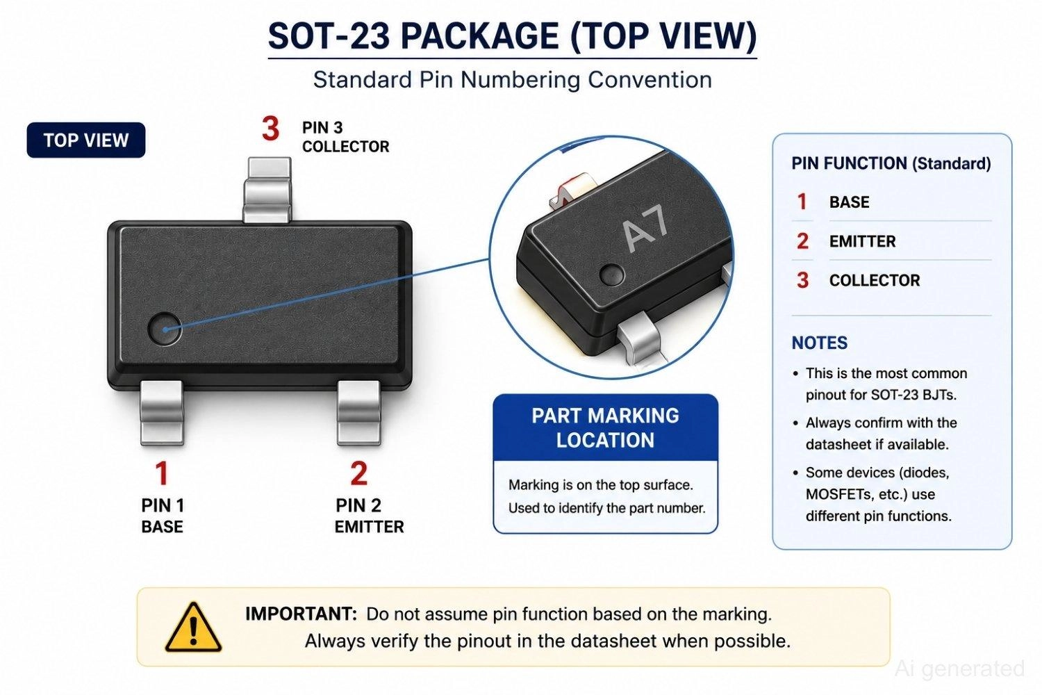
Figure: SOT-23 package top view with standard pin numbering convention.
Common Transistor Pin Identification Mistakes
- Testing the transistor while it is still on the PCB: Surrounding components like bypass capacitors, pull-up resistors, or inductors form parallel electrical paths. These paths bypass the transistor junction under test, leading to incorrect "shorted" or "open" readings. Always desolder the component first.
- Assuming the middle pin is always the base: This is a classic beginner mistake. While many common transistors like the 2N3904 or BC547 have specific layouts, many RF transistors or Japanese standard pinouts (like the 2SA1015) feature the base on Pin 3 (right side) or Pin 1 (left side). Always test, never assume.
- Mistaking a MOSFET for a BJT: If you attempt to identify the gate, drain, and source of a MOSFET using BJT diode-test steps, you will get highly confusing results (typically OL in almost all configurations due to the insulated gate). Make sure you are working with a BJT before applying these diode test routines.
- Confusing "OL" with a dead transistor: In diode mode, "OL" simply means no current is flowing. This is the correct, healthy response for any reverse-biased PN junction. It only indicates a blown transistor if it occurs when the junction should be forward-biased.
- Ignoring thermal effects during testing: Holding the transistor body tightly with your fingers while probing can warm up the silicon die. Since semiconductor junction voltage drop has a negative temperature coefficient (it decreases by approximately -2 mV per degree Celsius), body heat can cause readings to drift, making collector-emitter comparisons inaccurate.
Checking a Transistor with a Multimeter: Troubleshooting Guide
| Observed Reading | Possible Cause | Recommended Action |
|---|---|---|
| OL in all directions | Open-circuit failure (internal wire bond fused) | Replace the transistor |
| 0.00V in multiple directions | Short-circuit failure (junction melted due to overcurrent) | Replace the transistor |
| Conduction in both directions on one pair | Damaged junction | Replace the transistor |
| Symmetrical readings (no voltage difference) | Highly symmetrical structure or low-quality meter resolution | Use hFE mode or build the breadboard LED test circuit |
| Drifting or unstable readings | Poor probe contact, finger oils, or in-circuit loading | Clean the leads, isolate the part completely, and retest |
FAQs About Transistor Pin Identification
Q: Can I identify transistor pins without a datasheet?
Yes. By using a digital multimeter set to diode-test mode, you can systematically test all three pins to find the common base, determine if it is NPN or PNP based on probe polarity, and isolate the emitter and collector by comparing minor forward-voltage variances or using the meter's hFE mode.
Q: How do I find the base pin of a transistor using a multimeter?
Set your multimeter to diode-test mode. Keeping one probe fixed on one pin, touch the other probe to the remaining two pins. The single pin that exhibits a forward-bias voltage drop (typically 0.55 V to 0.75 V) to both other pins is the base.
Q: How do I tell NPN from PNP with a multimeter?
Once you identify the common base pin, check which probe is connected to it during forward conduction to the other two pins. If the Red (positive) probe is on the base, it is an NPN transistor. If the Black (negative) probe is on the base, it is a PNP transistor.
Q: What does OL mean on a multimeter during a transistor test?
OL stands for "Open Loop" or "Over Limit." It indicates that the multimeter is detecting an open circuit or infinite resistance. This is the normal and expected reading when testing a reverse-biased PN junction.
Q: Can I test a transistor without removing it from the circuit?
It is highly discouraged. In-circuit components connected to the transistor legs create alternative pathways for the multimeter's test current, yielding false voltage drops or indicating non-existent shorts. For precise results, desolder the transistor before testing.
Conclusion
Using a multimeter's diode-test mode is the most efficient and reliable way to identify BJT transistor pins and polarity without a datasheet. By mapping the two internal diode junctions, you can easily isolate the base, determine if it is NPN or PNP, and compare voltage drops to distinguish the collector from the emitter. While SMD packages like SOT-23 require extra caution due to layout variations, a systematic multimeter test prevents costly component damage and assembly errors.
For your next hardware project, you can easily streamline production by uploading your verified designs directly to the JLCPCB platform to get instant prototyping quote.
Popular Articles
• PCB X-Ray Inspection Explained: Non-Destructive Testing for PCB Assembly Quality Control
• Flying Probe Testing: Revolutionizing PCB Quality Assurance in Modern Electronics Manufacturing
• Solder Paste Inspection (SPI): A Complete Guide to Process Control in SMT Assembly
• What Is PCBA Testing? Complete Guide to Inspection Methods, Process, and Quality Control
• Automated Optical Inspection (AOI): Principles, Defects, and PCB Applications
Keep Learning
PCB X-Ray Inspection Explained: Non-Destructive Testing for PCB Assembly Quality Control
In the era of miniaturization, modern printed circuit boards (PCBs) face an invisible challenge: verifying the quality of solder joints hidden beneath components. With Ball Grid Array (BGA) packages featuring pitch sizes down to 0.3mm and Quad Flat No-lead (QFN) components concealing critical thermal connections, traditional optical methods are blind to the most critical failure points. PCB X-ray inspection has emerged as the definitive solution. This guide explores the technical foundations, applicat......
Flying Probe Testing: Revolutionizing PCB Quality Assurance in Modern Electronics Manufacturing
The process for manufacturing printed circuit boards (PCBs) includes a critical testing phase. Each board must undergo testing to ensure manufacturers detect every electrical or circuitry problem before leaving the center. When a PCB passes this testing, it further ensures that it performs reliably. The most common types of testing methods include in-circuit testing (ICT) and flying probe testing (FPT). 6 high-precision probes (needles), 4 on top and 2 on the bottom are programmatically able to contac......
Transistor Pin Identification Using a Multimeter: Complete Step-by-Step Guide
Identifying transistor pins correctly is one of the first checks every engineer, hobbyist, and EE student needs before placing a bipolar junction transistor (BJT) into a circuit. A wrong base, collector, or emitter assignment can destroy the part on first power-up or leave a prototype board silently non-functional. This guide explains how to identify transistor pins using a multimeter when no datasheet is available. The method works because a BJT is internally built from two PN junctions sharing a com......
Solder Paste Inspection (SPI): A Complete Guide to Process Control in SMT Assembly
In today's Surface Mount Technology (SMT) manufacturing world, the consistency of the solder paste deposit is the element that drives electrical performance, mechanical shear strength, and long-term reliability of assembled Printed Circuit Boards. The solder paste is the medium that bonds the component terminations to the copper pads on the PCB. Therefore, any variations in the solder paste deposit in terms of volume, thickness, or placement will drastically impact the quality of the solder joints in ......
What Is PCBA Testing? Complete Guide to Inspection Methods, Process, and Quality Control
In modern electronics, the performance and long-term reliability of a finished product are directly tied to its Printed Circuit Board Assembly (PCBA) quality control. Even small defects at the board level—such as microscopic solder cracks, misaligned components, or incorrect passive values—can cascade into costly field failures, product recalls, and long-term damage to a brand's reputation. High-quality PCBA is not achieved through a single final inspection; it is the result of a repetitive and system......
Automated Optical Inspection (AOI): Principles, Defects, and PCB Applications
What Is Automated Optical Inspection (AOI)? Automated Optical Inspection (AOI) is a machine-based inspection method that uses high-resolution cameras, controlled lighting, and image-processing software to automatically detect visual defects on printed circuit boards (PCBs). It is widely used in PCB fabrication and PCB assembly to inspect components, solder joints, and conductor patterns without physical contact. By comparing captured images with design data or reference models, AOI systems can quickly......