
What Is PCBA Testing? Complete Guide to Inspection Methods, Process, and Quality Control
12 min
- PCBA Testing: Pre-Assembly Verification
- PCBA Testing: In-Process Inspection
- PCBA Testing: Final Electrical & Functional Validation
- FAQ about PCBA Testing
- Conclusion: PCBA Testing
In modern electronics, the performance and long-term reliability of a finished product are directly tied to its Printed Circuit Board Assembly (PCBA) quality control. Even small defects at the board level—such as microscopic solder cracks, misaligned components, or incorrect passive values—can cascade into costly field failures, product recalls, and long-term damage to a brand's reputation.
High-quality PCBA is not achieved through a single final inspection; it is the result of a repetitive and systematic testing workflow that begins before the first reel of components is loaded and continues until every assembled board has demonstrated full functionality.
For complex, high-density designs, partnering with a manufacturer that implements advanced inspection and test methods is essential. At JLCPCB, we integrate rigorous, technology-driven PCBA inspection throughout the entire assembly process to ensure every board meets the highest standards of performance and reliability.
This guide outlines the best practices and advanced techniques used in a PCBA testing workflow—from component verification to final functional testing.
PCBA Testing: Pre-Assembly Verification
The most effective way to prevent defects is to ensure that only perfect components and PCBs enter the PCB assembly line. This foundational stage, known as incoming quality control (IQC), is a critical first line of defense.
1Incoming Quality Control (IQC) for Components
Every printed circuit board assembly (PCBA) begins with a Bill of Materials (BOM), and the integrity of the final product depends on the absolute accuracy of the components used. The incoming quality control (IQC) for the components is a comprehensive verification process that can occur at any stage of the assembly process, which includes:
- Authenticity and Part Number Verification: Components are validated against the BOM and manufacturer data sheets to confirm the part number and values (resistance, capacitance) and tolerances. This is a vital step to eliminate counterfeit or incorrect parts that can induce a failure, either immediately or latent.
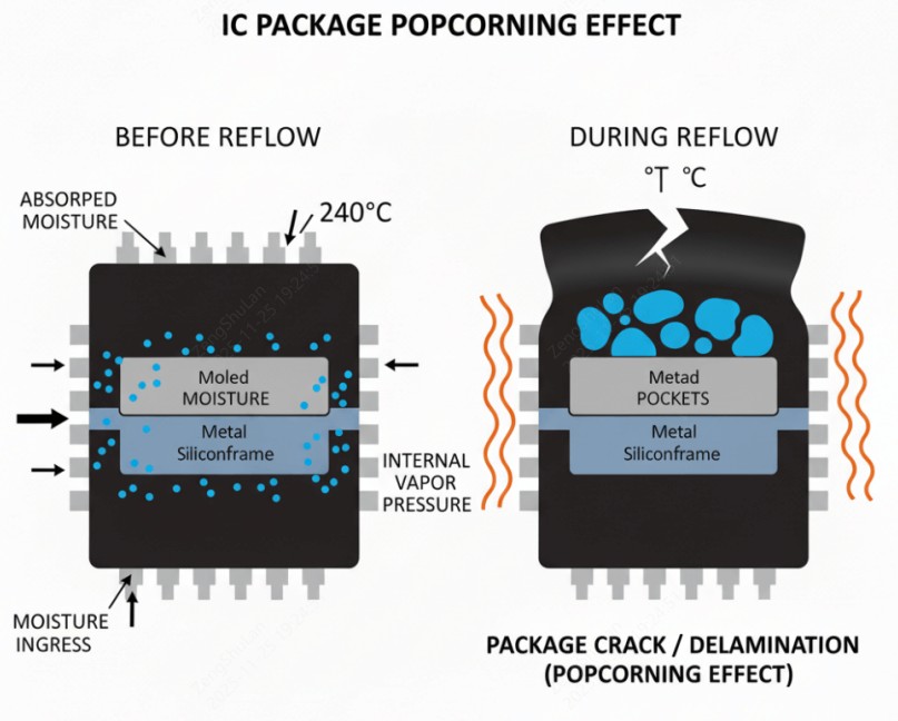
- Moisture Sensitivity Level (MSL) Management: Integrated circuits and certain passive components are hygroscopic, absorbing moisture from the surrounding air. Each component has an MSL rating, including its allowable exposure time ("floor life") outside of dry storage. During the high temperatures of the reflow soldering process, any moisture trapped in the parts will vaporize, creating significant internal pressure. The pressure can cause the package layers to delaminate, internal wire bonds to fail, or result in an explosive failure known as "popcorning".
Proper IQC involves verifying the MSL, checking dry pack seals, and baking any components that have exceeded their "floor life" to safely remove moisture before assembly.
JLCPCB offers a massive in-stock component sourcing and verification process, minimizing the risk of counterfeit or incorrect parts in PCB assemblies. We expertly manage MSL components through careful storage, tracking, and secure transport.
2Bare Board (PCB) Inspection
The bare PCB itself is a complex engineered product. Before it enters the SMT line, it must undergo its own set of quality control tests:
- Visual and Automated Optical Inspection (AOI): Each board will experience some form of inspection for surface defects such as scratches, contamination, or oxidation on the pads. In addition to visual inspections, AOI systems can also easily verify that trace widths and spacing are compliant with the design.
- Dimensional Checks: Critical dimensions, board thickness, and the diameter of plated through holes (PTH) are measured for mechanical compatibility and proper component fit. Warpage and twist are measured, as an excessively bowed board can cause major problems during solder paste printing and component placement.
- Electrical Testing (E-Test): This is arguably the most critical PCB test. A "bed-of-nails" fixture for high-volume runs, or a "flying probe" tester for prototypes, is used for E-Test to confirm the connectivity of the PCB. The E-Test ensures that each net that should be connected is connected and that no separate nets are shorted together.
- Solder Mask and Silkscreen Registration: The registration or alignment of the solder mask and silkscreen layers is checked. A solder mask that is not aligned can lead to solder bridging, while a silkscreen that is not aligned can cover pads or lead to incorrect component placement during manual assembly or rework.
| Potential Impact | Primary Detection Method | |
|---|---|---|
| Counterfeit IC | Complete or intermittent functional failure, reduced lifespan | Supplier verification, X-Ray Fluorescence (XRF) for materials, Decapsulation |
| Incorrect Component Value | Circuit malfunction, damage to other components | Part number verification, LCR meter measurement during IQC |
| Component Oxidation | Poor solderability, weak or non-existent solder joints | Visual inspection, Solderability testing |
| Excessive PCB Warpage | Poor solder paste stencil seal, component placement issues | Measurement against proper design standards (e.g., IPC-A-600) |
| PCB Internal Short/Open | Complete functional failure of the affected circuit | Electrical Testing (E-Test) |
PCBA Testing: In-Process Inspection
Once materials are verified, inspection will become a meaningful part of the SMT assembly line. Those in-process inspections allow for real-time feedback to identify defects at their source.
1Solder Paste Inspection (SPI)
Industry data consistently shows that 60-70% of all SMT defects can be traced back to the solder paste printing process. Therefore, inspecting the solder paste deposits before components are placed is one of the highest-leverage inspection steps.
Modern manufacturing relies on 3D SPI machines, which use laser triangulation to create a topographical map of the solder paste on every single pad. Unlike older 2D systems that only checked for area and bridging, 3D SPI provides precise quantitative data on:
- Volume: The total amount of solder paste, ensuring there's enough for a strong joint but not so much to risk bridging.
- Height: Critical for ensuring components will sit correctly in the paste.
- Area: The coverage of the paste on the pad.
- XY-Offset: The alignment of the paste deposit on the pad.
This data allows for immediate process correction if, for example, the machine detects a gradual decrease in paste volume, indicating a clogged stencil aperture.
2Automated Optical Inspection (AOI)
AOI systems utilize high-definition cameras and advanced image analysis software to autonomously scan printed circuit board assemblies and find defects. AOI is usually employed at two major points:
- Pre-reflow: checks for the correct placement of components, whether the component is present/absent, verifying that components are oriented correctly (diodes, electrolytic capacitors, integrated circuits, etc.), and ensuring tombstoning has not occurred before entering the reflow oven. Finding a defect at this stage makes rework much easier.
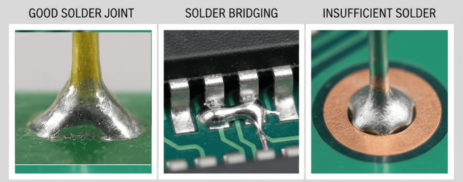
- Post-reflow: This is by far the most typical use of AOI. It inspects the quality of the solder joints, looking for defects such as solder bridges, insufficient solder, excess solder, and lifted leads.
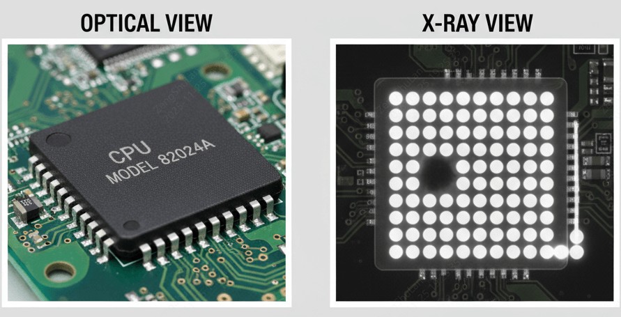
Although AOI is extremely effective for components with surface defects, it has a simple limitation: it cannot see what is hidden. Therefore, AOI is not applicable for inspecting solder joints under components such as BGAs and QFNs.
3Automated X-Ray Inspection (AXI)
Automated X-Ray Inspection (AXI) is the industry standard for evaluating solder joints that are not visible from the outside. AXI systems can image through an IC package—down to the silicon level—to reveal the solder balls of BGAs or the thermal pad and leads of QFN packages. AXI is essential for performing the following inspections:
- Solder Joint Integrity: looking for shorts, opens, or proper formation of the solder joint.
- Voids: identify gas bubbles that can be trapped inside the solder joint. Excessive voiding can compromise thermal and electrical performance and increase the risk of mechanical failure.
- Component Alignment: checks the ball pattern of a BGA to the PCB pads.
Advanced 3D AXI systems can even slice through the board digitally, isolating and inspecting individual layers on densely populated, double-sided assemblies.
PCBA Testing: Final Electrical & Functional Validation
Once a board is fully assembled, the last inspection phase is focused on checking overall quality and, crucially, on function.
Visual Inspection and IPC Standards
While certain automated systems are advanced, a trained eye of a human inspector is invaluable. Technicians perform a final visual check, looking for any subtle defects that machines might miss.
This inspection is not arbitrary; it is governed by rigorous in-house quality standards that align with global industry benchmarks. The most common benchmark is IPC-A-610, "Acceptability of Electronic Assemblies". This document provides the detailed, visual "rulebook" for what constitutes an acceptable solder joint, component placement, and overall assembly quality. It defines three classes of product:
- Class 1: General Electronic Products (e.g., consumer toys)
- Class 2: Dedicated Service Electronic Products (e.g., laptops, smartphones)
- Class 3: High-Performance/Harsh Environment Electronic Products (e.g., medical life support, aerospace, automotive)
JLCPCB's adherence to stringent, certified quality systems like ISO 9001:2015 and the automotive-grade IATF 16949:2016 ensures that these visual inspection processes are documented, repeatable, and traceable, providing a robust framework for delivering high-reliability assemblies.
| Class 1 (Target) | Class 2 (Acceptable) | Class 3 (Acceptable) | |
|---|---|---|---|
| End Joint Width | Width (W) ≥ 75% Lead (L) | W ≥ 50% L | W ≥ 75% L |
| Side Joint Length | Length (D) ≥ 3 × W | D ≥ 1.5 × W or 0.5mm | D ≥ 3 × W or 0.5mm |
| Solder Wetting | Well-wetted fillet visible | Wetting is evident | Well-wetted fillet visible |
IPC-A-610 Solder Joint Criteria for a Gull-Wing Lead
Note
Ultimately, the final determinant of a PCBA's quality is whether it works.
Flying Probe Test (FPT)
Flying Probe Test is well-suited for prototypes and low-volume PCB assembly. It employs 2-6 robotic probes that move across the board, touching test points to verify for shorts, opens, and accurate component values (such as resistors and capacitors). This method offers high flexibility and eliminates the need for custom fixtures, though the testing time per board is comparatively slower.
Functional Testing (FCT)
Functional testing can be considered the ultimate "go/no-go" test. It will simulate your PCBA's final operating environment. You can either create a custom fixture or use a test bench to power the board and communicate with it to validate its behavior against its design specifications.
For example, does the LED blink at the proper frequency? Is data being transmitted over the wireless module, and are the sensor readings accurate? FCT is assuring the entire system works as intended.
In-Circuit Testing (ICT)
In-Circuit Testing (ICT) is best for high-volume, mature products. It uses a custom "bed-of-nails" fixture to contact designated board test points. It will turn the board on and electrically test each component individually to verify the correct value, as well as check for shorts and opens. ICT delivers excellent fault coverage, but does have a heavier upfront fixture cost.
FAQ about PCBA Testing
Q: What is PCBA testing?
PCBA testing is the process of inspecting, measuring, and validating assembled circuit boards to ensure they function correctly. It includes SPI, AOI, AXI, flying probe testing, ICT, and functional testing.
Q: What are the main PCBA testing methods?
The main PCBA testing methods are:
- Solder Paste Inspection (SPI)
- Automated Optical Inspection (AOI)
- Automated X-Ray Inspection (AXI)
- Flying Probe Testing (FPT)
- In-Circuit Testing (ICT)
- Functional Testing (FCT)
Q: What is the main difference between Automated Optical Inspection (AOI) and Automated X-Ray Inspection (AXI)?
AOI uses visible light to detect external, surface-level defects such as incorrect component placement, polarity errors, and solder bridges.
AXI, on the other hand, uses X-ray imaging to inspect internal or hidden features—such as BGA solder balls, QFN thermal pads, voids, and insufficient solder beneath packages that AOI cannot see.
Q: Can Functional Testing (FCT) replace any of the inspection methods (AOI, ICT)?
No. Functional Testing complements AOI and ICT but does not replace them.
AOI and ICT are designed to detect manufacturing defects—such as opens, shorts, misplacements, and solder joint issues—while Functional Testing verifies whether the assembled board performs according to the intended electrical and system functions.
A robust quality workflow typically includes all three because each method addresses a different type of risk.
Q: How does complexity influence the PCBA inspection method?
As PCB complexity increases, the required level of inspection becomes more advanced.
Simple boards may only require manual visual checks and basic AOI.
However, dense, multilayer, or component-rich designs—especially those with hidden interconnects like BGAs, WLPs, or QFNs—require more sophisticated methods such as 3D SPI, 3D AOI, ICT, and AXI to properly verify solder joints and component integrity.
Conclusion: PCBA Testing
As we know, ensuring robust PCBA quality is not a single action but a comprehensive and deeply integrated strategy. From ensuring all components and bare boards are verified before assembly, using real-time SPI, AOI, and AXI data on the SMT line, and checking the final product against IPC and functional requirements, each inspection relies on the previous stage. This multi-layered approach is the only way to ensure the systematic elimination of defects, reduced field failures, and ultimately, provides the highest reliability in a final product.
Verify and assure the quality and reliability of your next electronics project. Upload your files for an instant quote and take advantage of our advanced inspection processes today.
Popular Articles
• PCB X-Ray Inspection Explained: Non-Destructive Testing for PCB Assembly Quality Control
• Flying Probe Testing: Revolutionizing PCB Quality Assurance in Modern Electronics Manufacturing
• Solder Paste Inspection (SPI): A Complete Guide to Process Control in SMT Assembly
• What Is PCBA Testing? Complete Guide to Inspection Methods, Process, and Quality Control
• Automated Optical Inspection (AOI): Principles, Defects, and PCB Applications
Keep Learning
PCB X-Ray Inspection Explained: Non-Destructive Testing for PCB Assembly Quality Control
In the era of miniaturization, modern printed circuit boards (PCBs) face an invisible challenge: verifying the quality of solder joints hidden beneath components. With Ball Grid Array (BGA) packages featuring pitch sizes down to 0.3mm and Quad Flat No-lead (QFN) components concealing critical thermal connections, traditional optical methods are blind to the most critical failure points. PCB X-ray inspection has emerged as the definitive solution. This guide explores the technical foundations, applicat......
Flying Probe Testing: Revolutionizing PCB Quality Assurance in Modern Electronics Manufacturing
The process for manufacturing printed circuit boards (PCBs) includes a critical testing phase. Each board must undergo testing to ensure manufacturers detect every electrical or circuitry problem before leaving the center. When a PCB passes this testing, it further ensures that it performs reliably. The most common types of testing methods include in-circuit testing (ICT) and flying probe testing (FPT). 6 high-precision probes (needles), 4 on top and 2 on the bottom are programmatically able to contac......
Transistor Pin Identification Using a Multimeter: Complete Step-by-Step Guide
Identifying transistor pins correctly is one of the first checks every engineer, hobbyist, and EE student needs before placing a bipolar junction transistor (BJT) into a circuit. A wrong base, collector, or emitter assignment can destroy the part on first power-up or leave a prototype board silently non-functional. This guide explains how to identify transistor pins using a multimeter when no datasheet is available. The method works because a BJT is internally built from two PN junctions sharing a com......
Solder Paste Inspection (SPI): A Complete Guide to Process Control in SMT Assembly
In today's Surface Mount Technology (SMT) manufacturing world, the consistency of the solder paste deposit is the element that drives electrical performance, mechanical shear strength, and long-term reliability of assembled Printed Circuit Boards. The solder paste is the medium that bonds the component terminations to the copper pads on the PCB. Therefore, any variations in the solder paste deposit in terms of volume, thickness, or placement will drastically impact the quality of the solder joints in ......
What Is PCBA Testing? Complete Guide to Inspection Methods, Process, and Quality Control
In modern electronics, the performance and long-term reliability of a finished product are directly tied to its Printed Circuit Board Assembly (PCBA) quality control. Even small defects at the board level—such as microscopic solder cracks, misaligned components, or incorrect passive values—can cascade into costly field failures, product recalls, and long-term damage to a brand's reputation. High-quality PCBA is not achieved through a single final inspection; it is the result of a repetitive and system......
Automated Optical Inspection (AOI): Principles, Defects, and PCB Applications
What Is Automated Optical Inspection (AOI)? Automated Optical Inspection (AOI) is a machine-based inspection method that uses high-resolution cameras, controlled lighting, and image-processing software to automatically detect visual defects on printed circuit boards (PCBs). It is widely used in PCB fabrication and PCB assembly to inspect components, solder joints, and conductor patterns without physical contact. By comparing captured images with design data or reference models, AOI systems can quickly......