Polyimide Flex PCB: A Complete Guide for Engineers
16 min
- Understanding Polyimide Flex PCB and Its Role in Flexible Electronics
- Polyimide Flex PCB Structure, Materials, and Key Properties
- Advantages and Applications of Polyimide Flex PCBs
- Polyimide Flex PCB Design and Manufacturing Considerations
- Why Choose JLCPCB for Polyimide Flex PCB Manufacturing
- Conclusion
- FAQs About Polyimide Flex PCB
A polyimide flex PCB can be folded about 285,000 times when the base film is 25 µm (1 mil) thick. Make that film 75 µm (3 mil), and the same MIT fold test gives up near 6,000 cycles. Bending is a strain problem, not a material problem. Copper sits above the center of the stack, so a bend forces it to stretch around the longer outer path.
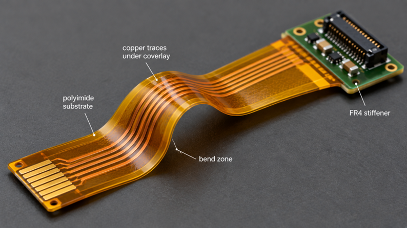
Figure 1: A polyimide flex circuit folded tight, with a stiffener holding the connector
A thicker stack places the copper farther out, resulting in more stretch at the same radius. The film elongates 72% before it breaks, but the copper on it gives up far sooner. The foil fails first, so thickness drives almost every flex decision. This guide covers the four-layer construction and the material data behind it. It then covers the applications, the bend radius, and the copper rules a fabricator can actually hold.
Understanding Polyimide Flex PCB and Its Role in Flexible Electronics
Flexible electronics exist because one polymer works across a temperature range that no other cheap film survives. Polyimide is that polymer, and most of what a flex circuit can do follows from it.
What is a Polyimide Flex PCB and How Does It Work?
A polyimide flex PCB is a circuit built on thin polyimide film instead of rigid glass-epoxy. Copper foil is bonded to that film, and a second polyimide layer is laminated over the traces as protection. Finished builds run 0.07 mm to 0.2 mm (2.8 mil to 8 mil), so the whole board folds.
Electrically, nothing changes, but the difference is mechanical. When the board bends, the outside of the curve stretches and the inside compresses. A thin neutral plane between them does neither, which is why copper placed near it barely strains. Polyimide is not a coating over some other substrate. It is the structural material here, so its 231 MPa (33,500 psi) tensile strength is what allows a 25 µm film to withstand a connector push without tearing.
Why Polyimide Is Widely Used as a Flexible PCB Material
Polyester (PET) film is cheaper and bends just as well, but it softens near 80 °C. It cannot be reflowed much above 150 °C, which rules it out for soldered assemblies. Polyimide has no melting point, and its glass transition temperature ranges from 360 °C to 410 °C, so a 260 °C lead-free peak passes straight through.
Against FR4, the question is less about heat and more about what the board has to do. FR4 is stiffer, drier, and cheaper per square inch, so it is usually selected based on how to select the Tg of a PCB. Polyimide is thinner, foldable, and dimensionally much closer to the copper it carries.
| Property | Polyimide (Kapton HN) | Standard FR4 | What It Means for Your Board |
| Glass transition | 360 to 410 °C | 130 to 180 °C | Nothing softens at reflow, so Tg stops mattering |
| Dielectric constant, 1 kHz | 3.4 | 4.2 to 4.7 | Traces run wider for the same impedance |
| Thermal conductivity | 0.12 W/mK | about 0.3 W/mK | Heat leaves through copper, never the substrate |
| Moisture at 50% RH | about 1.8% | about 0.1 to 0.2% | Flex panels need a bake before reflow |
Polyimide Flex PCB Structure, Materials, and Key Properties
A flex build is a short stack, but every layer in it shows up later as a bend life or as a field failure. The construction also decides how thin the finished circuit can be.
Polyimide Substrate, Copper Foil, Coverlay, and Stiffeners
Four layers make up almost every polyimide flexible circuit, and they serve two functions. Two of them carry the circuit, while two protect and support it.
- Polyimide substrate: the base film, normally 25 µm or 50 µm (1 mil or 2 mil), specified to IPC-4204.
- Copper foil: 12 µm to 35 µm (1/3 oz to 1 oz), rolled, annealed, or electrodeposited.
- Coverlay: a second polyimide film of 12.5 µm to 25 µm (0.5 mil to 1 mil), laminated over the copper.
- Stiffeners: local backing in polyimide, FR,4, or steel, bonded under connectors so those areas cannot flex.
Substrate and foil set bend life together, because they are the two layers that take the strain. A thinner base film puts the copper nearer the neutral plane, which is why it folds many times more often. Liquid photoimageable solder mask is brittle and cracks the first time a board folds, so flex uses a laminated polyimide coverlay instead. Stiffeners do the opposite job, since a 0.2 mm (8 mil) FR4 pad gives the connector insertion force something rigid to push against.
Adhesive vs. Adhesiveless Polyimide Flex PCB Construction
There are two ways to get copper onto polyimide, and the difference is a 12.5 µm to 25 µm (0.5 mil to 1 mil) glue layer. Adhesive-based laminate bonds rolled foil to the film with acrylic or epoxy. Adhesiveless laminate puts copper straight onto the film, so nothing sits between them.
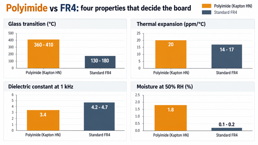
Figure 2: Cross-sections of adhesive and adhesiveless polyimide laminate
That glue layer expands far more in the z-axis than the materials around it, because a soft unreinforced polymer has nothing holding it back. When the panel goes through reflow, the adhesive pushes outward against the plated barrel of any via crossing it, which is where barrel cracks start. Removing the adhesive removes thickness, too, so an adhesiveless build finishes thinner and bends tighter. JLCPCB supports both constructions, but adhesiveless is what to specify for anything that flexes in service.
Key Thermal, Mechanical, and Electrical Properties of Polyimide
The values below are DuPont Kapton HN, since most flex laminates are built on that grade. Your board inherits these limits, regardless of whether the brand appears on the order.
Figure 3: Polyimide and FR4 compared across Tg, expansion, Dk, and moisture.
| Property | Typical value, Kapton HN | What It Means for Your Board |
| Usable temperature range | -269 °C to 400 °C (-452 °F to 752 °F) | Survives reflow and under-hood ambients |
| MIT fold endurance | 285,000 cycles at 25 µm, 6,000 at 75 µm | Thin film is what buys dynamic bend life |
| Thermal expansion | 20 ppm/°C | Close to copper at 17 ppm/°C, so features hold position |
| Thermal conductivity | 0.12 W/mK | The substrate cannot act as a heatsink |
| Dielectric strength | 303 kV/mm (7,700 V/mil) at 25 µm | Insulates past any board-level voltage |
| Moisture at 50% RH | about 1.8% by weight | Bake before reflow, or the water flashes to steam |
The 0.12 W/mK figure means copper pours have to spread the heat, since the substrate will not. Moisture at 1.8% means a pre-bake is not optional before a 260 °C reflow. The choice of adhesive determines whether your vias survive thermal cycling. Film thickness decides whether the copper survives the bend, so the two are specified together.
Advantages and Applications of Polyimide Flex PCBs
Three properties explain why designers pay the flex premium: heat tolerance, foldability, and low mass. Each maps onto a different family of products, so the application list below follows from them.
High-Temperature Resistance, Flexibility, and Lightweight Construction
Heat tolerance is what rules out the cheaper films. Polyimide works continuously near 200 °C and reaches a 260 °C peak without dimensional change. Solder is involved in every assembled board, so that one difference settles the material choice.
Flexibility and low mass come from the same source: thickness. A two-layer flex at 0.11 mm (4.3 mil) is roughly one-fifteenth the thickness of a 1.6 mm (63 mil) rigid board, so the finished tail weighs very little. Thin also means the circuit follows a shape instead of dictating one, so a tail can wrap a housing or run through a hinge rather than forcing a flat rectangle.
Reliability Benefits for Repeated Bending and Harsh Environments
Every connector and crimp is a place where a product can fail, so flex removes them wholesale. One circuit replaces a harness and two connectors, which deletes dozens of mechanical interfaces. That is usually a bigger gain than the material itself brings.
Where the circuit moves, life depends on strain rather than time. Rolled annealed foil has grains flattened into the plane of the sheet, like a stack of paper. It elongates by 20% to 45% before fracture, whereas electrodeposited foil elongates by 4% to 11%. RA copper is therefore mandatory once bending repeats. Harsh environments suit polyimide because it stays chemically stable and does not embrittle in the cold. Vibration is handled the way bending is, since the tail moves with the assembly instead of passing movement into a solder joint.
Common Applications in Consumer Electronics, Automotive, Medical, and Industrial Devices
Four sectors buy most of the world's polyimide flex, but each buys it for a different reason, and that reason decides which property binds the design.
- Consumer electronics: camera module tails, display connections, and folding-phone hinges, where bend life drives the design.
- Automotive: LED tail lamps, ADAS camera modules, and cell-monitoring flex in EV battery packs, at ambients reaching 125 °C.
- Medical: catheters, hearing aids, and endoscope heads, where the circuit fits a tube a few millimeters across.
- Industrial: printer carriages, robot joints, and instrumentation, where one joint moves for years.
Consumer and automotive pull the material in opposite directions. A folding-phone hinge is a dynamic bend problem counted in hundreds of thousands of cycles, so it requires the thinnest film and RA copper. A tail lamp flex barely moves, but it sits near 125 °C for a decade, which makes thermal aging the deciding factor. Medical and industrial products add constraints that the first two never see. A catheter circuit has to clear biocompatibility testing and survive autoclave cycles at 134 °C.
Polyimide Flex PCB Design and Manufacturing Considerations
Most flex problems are settled before the board reaches the fab, in three decisions: stack thickness, how copper crosses the bend, and where the rigid areas sit. Process limits sit on top, so a layout that clears DRC can still be unbuildable.
Choosing the Right Thickness, Copper Type, and Layer Count
On a rigid board, PCB thickness is mostly a mechanical decision. On flex, it sets bend radius, handling, and layer count at once, because every added copper layer stiffens the bend. Copper weight is a current decision, not a bending decision, and the flex PCB stackup design guide covers how the two interact. Foil at 12 µm (1/3 oz) carries roughly a third of the current that 35 µm (1 oz) carries at the same width. Power flex therefore lands at 35 µm, signal flex at 12 µm or 18 µm.
| Application | Film | Copper | Layers | JLCPCB Build |
| Folded once during assembly | 50 µm (2 mil) | ED or RA, 35 µm (1 oz) | 1 to 2 | 0.12 mm (4.7 mil) |
| Occasional flexing for service | 25 µm (1 mil) | RA, 18 µm (0.5 oz) | 1 to 2 | 0.11 mm (4.3 mil) |
| Continuous dynamic motion | 25 µm (1 mil) | RA, 12 µm (1/3 oz) | 1 | 0.07 mm (2.8 mil), adhesiveless |
| Dense routing, limited bending | 50 µm (2 mil) | RA or ED, 18 µm (0.5 oz) | 4 | 0.2 to 0.45 mm (8 to 18 mil) |
Bend Radius, Trace Layout, and Stiffener Design Requirements
Bend radius is specified as a multiple of total stack thickness, and IPC-2223 sets the multipliers. A static single-layer bend needs 6 times the thickness, a two-layer bend 12 times, while dynamic bending needs 100 times or more. The JLCPCB flexible PCB bend radius guide adds another 20%-30% margin.
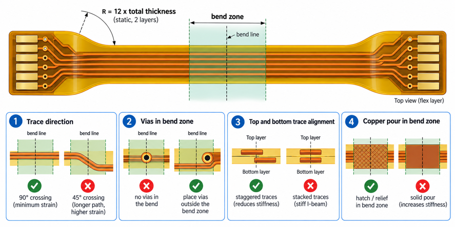
Figure 4: Bend zone layout with 90-degree crossings and staggered copper
Run those multipliers on a 0.11 mm (4.3 mil) two-layer flex. A static fold needs 1.32 mm (52 mil), or about 1.7 mm (67 mil) once the margin is added. The same circuit used dynamically needs 11 mm (433 mil), so a dynamic tail usually gets redesigned as a single layer.
- Cross the bend line at 90 degrees. A trace at an angle takes a longer path and higher strain.
- Keep vias and pads out of the bend zone. A plated hole is a stress riser, so it cracks first.
- Stagger copper on a two-layer flex. Stacked traces form a stiff I-beam.
- Hatch any ground plane. A solid pour work-hardens, while a hatched pour keeps bending.
Stiffeners decide where the board can move at all. Bond one under every connector and every through-hole part, because that force would otherwise flex the film at a solder joint. JLCPCB offers polyimide stiffeners from 0.1 mm to 0.25 mm (4 mil to 10 mil), FR4 from 0.2 mm to 1.6 mm (8 mil to 63 mil), and steel from 0.1 mm to 0.3 mm (4 mil to 12 mil).
From Circuit Patterning and Lamination to Coverlay and Surface Finishing
Flex fabrication follows the rigid process in outline and differs at every handling step, because a 25 µm panel cannot support itself. Material is dried before it is imaged, since polyimide holds roughly 1.8% water. That water shifts dimensions as the panel heats.
- Bake and drill: Panels are dried, then vias are drilled or laser-cut to 0.1 mm (4 mil).
- Plate: Electroless copper and electroplating build the barrel joining the layers.
- Image and etch: Photoresist transfers the artwork, and exposed copper is etched away.
- Laminate the coverlay: Pre-cut polyimide is pressed on under heat.
- Finish and test: ENIG plates the pads, then a flying-probe test the circuit before profiling.
Coverlay openings are where new flex designers get caught. They are cut mechanically before lamination rather than photo-imaged, so each carries a registration tolerance. Pad openings are therefore drawn more generously than solder mask openings. ENIG is the practical finish here, because a HASL air knife would deform the film. Coverlay is drawn as a mechanical layer, not as a solder mask.
Why Choose JLCPCB for Polyimide Flex PCB Manufacturing
A flex design is only as good as the shop's control over thin material, because polyimide punishes loose registration faster than FR4 does.
Precision FPC Fabrication with Reliable Materials and Tight Manufacturing Control
JLCPCB builds polyimide flex in 1, 2, and 4-layer constructions, on 25 µm and 50 µm film. Polyimide is offered as a flexible material rather than a rigid substrate, so a rigid polyimide board is not something to plan around.
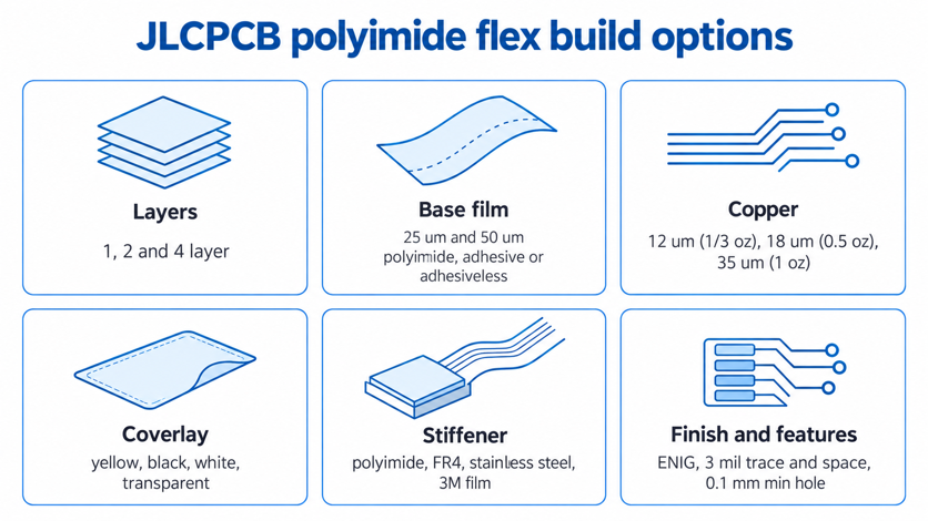
Figure 5: JLCPCB polyimide flex build options, from film and copper to coverlay.
The line holds 3 mil (0.076 mm) trace and space on 12 µm copper and 4 mil (0.1 mm) on 35 µm. Thicker foil etches with more undercut, so the finest rules only apply to the thinnest copper. Minimum hole size is 0.1 mm (4 mil) at ±0.08 mm (3 mil). Coverlay and stiffener options come from one fixed list on every order, so a repeat build stays repeatable. Coverlay is yellow, black, white, or transparent, stiffeners are polyimide, FR4, steel, or 3M film, and the finish is ENIG.
Rapid Prototyping, DFM Support, and Scalable Polyimide Flex PCB Production
Quoting is where a flex project stalls, because price depends on stackup, coverlay, and stiffener choices. Upload your Gerbers and the JLCPCB quote page prices the build directly, with each stackup option listed as you pick it.
DFM review then catches the flex-specific errors, because rigid design rules never flag them. Vias inside a bend zone, coverlay openings drawn as solder mask, and a missing stiffener all show up there. Assembly parts come from the JLCPCB parts library. Prototype quantities exist to prove the stackup. Production quantities reuse that stackup and tooling, so nothing needs re-qualifying at volume.
Conclusion
Polyimide flex PCB design comes down to a strain budget. Anything that thins the stack or moves copper toward the neutral plane buys bend life, while every added layer spends it. Flex keeps shifting from a packaging convenience to a structural choice as wearables, EV packs, and surgical instruments keep shrinking. When the design is ready to build, JLCPCB covers 1 to 4-layer polyimide flex on 25 µm and 50 µm film, with DFM review before any panel is cut.

FAQs About Polyimide Flex PCB
Q: Can a polyimide flex PCB be used as a rigid board?
Ans: No. Polyimide is supplied as a thin film with no rigidity of its own, so JLCPCB offers it as a flexible material rather than a rigid substrate. Bond stiffeners under any area that must stay rigid.
Q: Why does a flex circuit have to be baked before soldering?
Ans: Polyimide holds roughly 1.8% of its weight in water at normal room humidity. That water turns to steam at a 260 °C reflow peak, so it can blister the coverlay or lift copper. Panels are typically baked for one to two hours at 120 °C first.
Q: Can a flex circuit be bent after assembly, or must it be formed first?
Ans: Form the bend during assembly and leave it formed. Copper work-hardens every time it is bent, so a circuit designed for one static fold loses life if it is straightened and re-bent.
Q: Is polyimide the same thing as Kapton?
Ans: Kapton is DuPont's brand of polyimide film, the way a grade name refers to one maker's version of a generic material. Most published flex data, including the numbers here, comes from Kapton HN.
Q: Does a polyimide flex PCB cost more than the same circuit in FR4?
Ans: Yes. The film, the coverlay lamination step, and the extra handling all cost more than their FR4 equivalents, while the copper costs the same as for FR4. Shrinking the flex area saves more than dropping a layer.

Popular Articles
• Understanding the Basics of Electronic Devices and Circuits
• Understanding Digital Circuit Timing: Setup Time, Hold Time, Contamination Delay & Clock Skew
• PCBs Explained: A Simple Guide to Printed Circuit Boards
• Guide to the Top 10 Commonly Used Electronic Components
• Digital 101: Fundamental Building Blocks of Digital Logic Design
Keep Learning
Polyimide Flex PCB: A Complete Guide for Engineers
A polyimide flex PCB can be folded about 285,000 times when the base film is 25 µm (1 mil) thick. Make that film 75 µm (3 mil), and the same MIT fold test gives up near 6,000 cycles. Bending is a strain problem, not a material problem. Copper sits above the center of the stack, so a bend forces it to stretch around the longer outer path. Figure 1: A polyimide flex circuit folded tight, with a stiffener holding the connector A thicker stack places the copper farther out, resulting in more stretch at th......
Flex PCB Bend Radius: Calculation, Minimum Radius & Design Guidelines
Flex PCB bend radius is the one dimension on an FPC that no design rule check will catch. Bend the circuit tighter than its material allows; the outer copper stretches from its elongation limit, and then it cracks. Figure 1: A flex circuit formed around a mandrel, with bend radius and stack thickness A flex circuit bends around a neutral axis near the middle of its stack. Copper below that line is squeezed, and copper above it is pulled. So the further a layer sits from the line, the harder it is to w......
Flexible Circuit Connector: Types, Features & Selection Guide
A flexible circuit connector clamps onto the bare copper at the end of a flex circuit, so nothing is soldered at that joint. The tail slides into the housing, and an actuator presses a row of spring contacts onto the pads. Every connector is built around one tail thickness. TE's 0.5 mm pitch 2328702 family expects 0.30 mm (12 mil) of flex, because the contact beams are deflected by exactly that dimension. Figure 1: Cross-section of a 0.5 mm pitch FPC connector with the tail inserted Feed it a bare sin......
FPC vs FFC: Understanding the Key Differences Between Flexible Circuit Technologies
The FPC vs FFC decision is really a question about how the copper was made. An FFC consists of flat copper strips laminated between two PET films. Every conductor runs straight from end to end at one fixed pitch, because nothing in that process can make a trace turn or branch. An FPC starts as copper-clad polyimide and is etched exactly like a rigid board. Traces can turn, taper, split onto a second layer, and land under a soldered component. The finished circuit can be as thin as 0.1 mm (4 mil). Figu......
A Comprehensive Guide to Capacitor ESR: What It Is, Good Values, and How to Measure It
Key Takeaways Definition: Capacitor ESR (equivalent series resistance) is the single resistance that represents the losses inside a real capacitor, from its electrodes, terminations, electrolyte, and dielectric. Why It Matters: Ripple current flowing through the ESR produces a ripple-voltage step on the supply rail and I²R heating in the capacitor, which limits the capacitor's ripple-current rating and service life. Conditions Matter: ESR varies with frequency, temperature, capacitance, case size, and......
Understanding IPC-6012 Standards for High-Reliability Rigid PCB Fabrication
Key Takeaways IPC-6012 vs. IPC-A-600: IPC-6012 is the binding specification, while IPC-A-600 is only for visual reference. Class 2 vs. Class 3: Class 3 requires thicker copper (25μm vs. 20μm) and zero plating voids. Coupon Verification: Quality is tested by microsectioning panel coupons after thermal stress. Upfront Callout: Specify the class on drawings upfront; boards cannot be upgraded later. IPC-6012 is the line on your fabrication drawing that decides what your supplier is allowed to ship. Most d......