Flex PCB Bend Radius: Calculation, Minimum Radius & Design Guidelines
16 min
- Understanding Flex PCB Bend Radius
- How to Calculate the Minimum Flex PCB Bend Radius
- Static vs. Dynamic Flex PCB Bend Radius
- What Factors Affect Flex PCB Bend Radius?
- Flex PCB Bend Radius Design Guidelines
- How JLCPCB Supports Reliable Flex PCB Manufacturing
- Conclusion
- FAQs About Flex PCB Bend Radius
Flex PCB bend radius is the one dimension on an FPC that no design rule check will catch. Bend the circuit tighter than its material allows; the outer copper stretches from its elongation limit, and then it cracks.
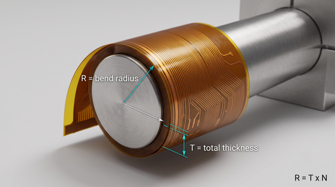
Figure 1: A flex circuit formed around a mandrel, with bend radius and stack thickness
A flex circuit bends around a neutral axis near the middle of its stack. Copper below that line is squeezed, and copper above it is pulled. So the further a layer sits from the line, the harder it is to work. Doubling the thickness doubles the strain at the same radius. That is why every published minimum is a multiple of thickness rather than a fixed millimeter value. A crack from that strain can still pass a bench test, because it opens only while the circuit is bent.
This guide covers the R = T x N formula and the static and dynamic minimums drawn from IPC-2223. It then works through the factors that drive those numbers and the layout rules that protect the bend area.
Understanding Flex PCB Bend Radius
Bend radius is quoted as a minimum, and it is measured to the inside face of the curve. Both halves matter because a figure taken from the wrong face is wrong by half a thickness.
What Is Flex PCB Bend Radius?
Flex PCB bend radius is the radius of the curve that a flexible circuit is formed. It is measured from the center of the bend to the innermost surface of the flex. Manufacturers publish it as a minimum, because below that figure, the copper is damaged rather than deformed. The figure is always a multiple of the circuit's total thickness, so there is no universal answer in millimeters. Total thickness means the whole stack inside the bend zone. That means base polyimide, copper on every layer, any adhesive, and coverlay on both faces.
Why Bend Radius Matters for Flex PCB Reliability
Bending a flex stretches the copper on the outside of the curve and compresses the copper inside. Between them sits the neutral axis, the plane whose length does not change. The strain grows with distance from it, so the outermost copper always works hardest.
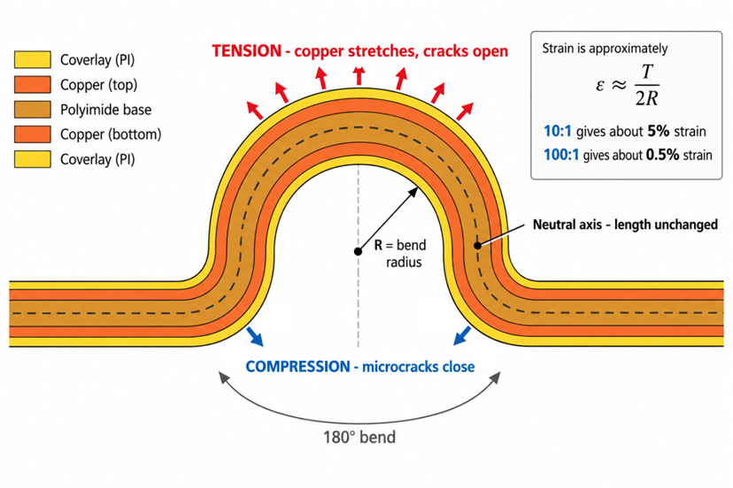
Figure 2: Cross-section of a bent flex, showing the neutral axis, and tension
Surface strain is roughly the thickness divided by twice the radius. A 10:1 bend, therefore, works the outer copper to about 5%. Rolled annealed copper stretches around 16% before it tears, so one bend at that ratio is comfortable. Repeated bending fails far earlier, because fatigue cracks grow at the strain the foil absorbs once without complaint. A dynamic flex needs a working strain near 0.5%. That is the whole reason the dynamic ratios are ten times larger.
How to Calculate the Minimum Flex PCB Bend Radius
Calculating a flex PCB's bend radius requires only one multiplication. The work is in choosing the two numbers. Get either one wrong, and the answer is off by a factor of ten.
Flex PCB Bend Radius Formula: R = T x N
The minimum flex PCB bend radius is R = T x N. The total thickness of the flexible section is multiplied by a ratio set by construction and bend type.
- R is the minimum bend radius, measured to the inside surface of the bend.
- T is the total thickness of the flex in the bend zone, coverlay, and adhesive included.
- N is the ratio for your construction and bend type, from 6:1 for a one-time crease up to 150:1 for a double-layer dynamic flex.
Designers usually get T wrong by taking it from the rigid section of a rigid-flex board. Only the flexible section bends, so measure the stack where the bend actually happens.
Flex PCB Bend Radius Calculation Example
Working the formula on a two-layer polyimide flex shows how far apart the two answers land. The stack is 18 µm (0.7 mil) copper on both faces of a 50 µm (2 mil) base. Coverlay adds 25 µm (1 mil) on each side.
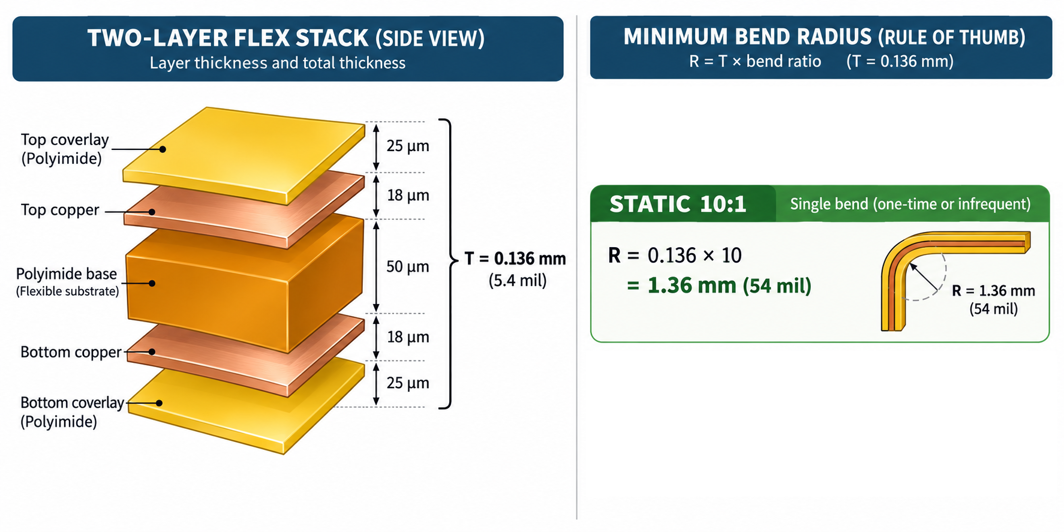
Figure 3: The two-layer stack summed to T, multiplied by the static and dynamic ratios.
- Add the stack: 18 + 50 + 18 + 25 + 25 µm gives T = 0.136 mm (5.4 mil).
- Pick N: A double-layer circuit bent once at assembly uses a 10:1 ratio.
- Multiply: R = 0.136 mm x 10 = 1.36 mm (54 mil).
- Repeat for dynamic use: At 150:1, the same circuit needs 20.4 mm (803 mil).
The two results are fifteen times apart on one circuit. Bend type, therefore, outweighs every material choice made afterward. If the mechanism cannot give 20 mm (787 mil) of clearance, drop that section to single-layer flex.
Flex PCB Bend Radius Chart by Thickness and Layer Count
Ratios increase with layer count because each additional copper layer is farther from the neutral axis. The chart applies the IPC-2223 figures to the FPC stackups JLCPCB builds most often.
| Construction and Total Thickness | Static Minimum Radius | Dynamic Minimum Radius | What This Means for Your Design |
| 1 layer, 12 µm copper, 0.10 mm (4 mil) | 1.0 mm (39 mil) at 10:1 | 10 mm (394 mil) at 100:1 | The only build for a tight fold or high cycle count |
| 1 layer, 35 µm copper, 0.13 mm (5 mil) | 1.3 mm (51 mil) at 10:1 | 13 mm (512 mil) at 100:1 | Heavier copper for current, paid for with a wider bend |
| 2 layer, 18 µm copper, 0.14 mm (5.5 mil) | 1.4 mm (55 mil) at 10:1 | 20 mm (800 mil) at 150:1 | Routing density doubles, dynamic radius grows by half |
| 4 layer, 0.30 mm (12 mil) | 6.0 mm (236 mil) at 20:1 | Not recommended | Move the bend to a 2-layer section or rigid-flex tail |
Static minimums stay small enough to design around, while dynamic minimums grow large enough to dictate the enclosure. The formula gives you a floor, not a target. Design two or three times above it where you can, so the flex stops being the part that fails first.
Static vs. Dynamic Flex PCB Bend Radius
Static and dynamic bends fail by different mechanisms, so they take different ratios from the same formula. Deciding which one you have comes before any routing.
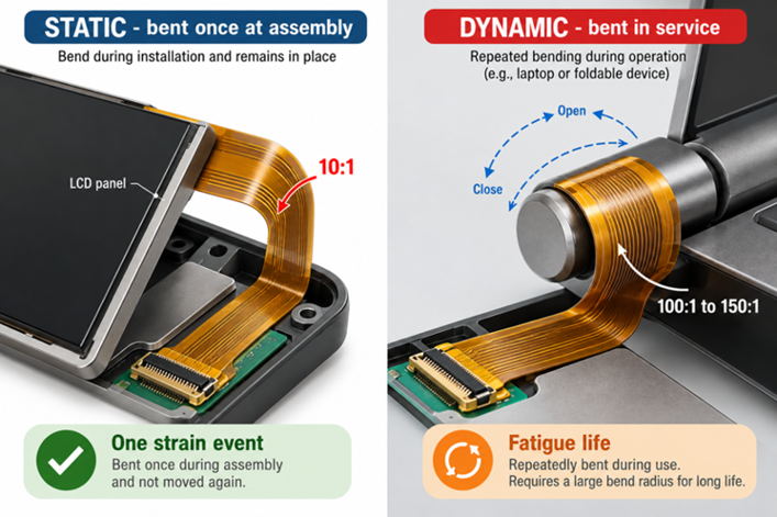
Figure 4: A static fold behind a display next to a dynamic bend at a hinge.
Static Flex PCB Bend Radius for One-Time Bending
A static bend is formed once during assembly and then holds that shape for life. IPC-2223 puts the floor at 10 times the total thickness for single and double-layer flex. Multilayer needs 20 times. Copper survives it because a single strain event near 5% sits well inside its elongation limit. A one-time crease folded flat against a stiffener can go down to 6 times the thickness. That applies only to single-layer circuits, and only where the copper faces inward.
Dynamic Flex PCB Bend Radius for Repeated Bending
A dynamic bend flexes repeatedly in service, so the limit is fatigue life rather than one strain event. Ratios jump to 100:1 for single-layer flex and 150:1 for double-layer. Multilayer is not recommended in a dynamic zone at all. Each extra layer moves copper further from the neutral axis, which raises strain at the same radius and sharply shortens life. Printer head cables and laptop hinge harnesses use single-layer flex with rolled annealed copper for that reason.
How to Choose the Right Bend Radius for Your Application
The mechanism, rather than the layout, determines the bend type, so settle on it before routing. The table maps four common applications onto the ratio each one needs.
| Application | Bend Type | Ratio to Use | What This Decides |
| The LCD tail folded behind the display at assembly | Static, one bend for life | 10:1, single or double layer | A 0.12 mm (4.7 mil) flex needs only 1.2 mm (47 mil) of clearance |
| Camera ribbon creased against a stiffener during installation | One-time crease | 6:1, single layer only | Copper must face the inside of the crease |
| Laptop lid harness, tens of thousands of cycles | Dynamic, low-cycle | 100:1 to 150:1 | Hinge diameter, not trace width, drives the layout |
| Printer head cable, millions of cycles at speed | Dynamic, high-cycle | 100:1 with rolled annealed copper | Single layer only, with hatched copper in the bend |
The right-hand column moves further than the ratio does, because a dynamic bend hands the radius decision to the mechanical designer. Static bends are a clearance problem you solve in the enclosure. Dynamic bends are a lifetime problem you solve in the stackup.
What Factors Affect Flex PCB Bend Radius?
Three properties of the circuit decide where its minimum sits, and they compound rather than add. All three are fixed at stackup, so none of them can be recovered later in routing.
- FPC thickness and layer count directly determine the strain, because both determine how far the copper sits from the neutral axis.
- Copper type and copper thickness set how much of that strain the foil absorbs before it cracks.
- Material construction and bend direction decide which side of the bend the copper ends up on.
How FPC Thickness and Layer Count Affect Bend Radius
Total thickness enters the formula directly. A stack growing from 0.10 mm (4 mil) to 0.20 mm (8 mil) doubles the minimum radius on its own. Layer count then raises the ratio on top of that, so the two effects multiply. A four-layer flex at 0.30 mm (12 mil) needs 6.0 mm (236 mil) of static radius. A single-layer circuit needs 1.0 mm (39 mil) for the same job. Splitting the flex into two thinner tails is usually cheaper than enlarging the hinge. The trade-offs mirror those in choosing PCB thickness on a rigid board.
How Copper Type and Copper Thickness Affect Flexibility
Copper foil comes in two grain structures, and the difference decides whether a circuit survives repeated bending. Rolled annealed foil is rolled into long grains lying flat in the plane of the sheet. Electrodeposited foil grows in columns standing perpendicular to it, and those columns crack apart.
Foil weight matters as much as grain structure, because thicker copper sits further from the neutral axis. Dropping from 35 µm (1 oz) to 12 µm (1/3 oz) through the bend zone cuts strain directly. JLCPCB lists 12 µm as a standard FPC option.
| Copper Type | Typical Elongation | Suited To | What This Means for Your Bend |
| Rolled annealed (RA) | About 16% | Static and dynamic bends | The default for any flex that moves in service |
| Electrodeposited (ED) | About 11% | Static bends only | Fine for a one-time fold, wrong for a hinge |
| High-ductility ED (HDED) | Between the two | Light dynamic use | A cost compromise when the RA lead time is long |
How Material Construction and Bend Direction Affect Flex PCB Reliability
Adhesive-based laminates bond copper to polyimide through an acrylic layer. That layer adds 25 µm (1 mil) or more per interface. Adhesiveless construction removes it, so the stack is thinner and the copper sits closer to the neutral axis.
The bend direction decides which copper layer takes the tension. On a single-layer flex, the copper should face the inside of the curve. Compression closes a microcrack, whereas tension opens it, so the same circuit lasts longer bent one way. Adhesiveless construction buys a smaller radius through the stackup. Bend direction buys the rest, and it costs nothing but a note on the fab drawing.
Flex PCB Bend Radius Design Guidelines
Three layout rules determine whether a bend area survives the product's life. They sit on top of your normal PCB design rules rather than replacing them.
- Keep vias, pads, and components out of the bend zone, because a plated hole is a rigid inclusion in a sheet that has to stretch.
- Avoid sharp corners and abrupt width changes, because strain concentrates wherever the geometry changes suddenly.
- Specify bend cycles, angle, and installation conditions, because a fabricator cannot infer any of them from the Gerbers.
Keep Vias, Pads, and Components Away From Bend Areas
A plated through hole inside a bend zone is the most common cause of flex failure. The copper barrel cannot stretch with the polyimide around it. Strain concentrates at the knee where the barrel meets the pad, so the crack starts there.
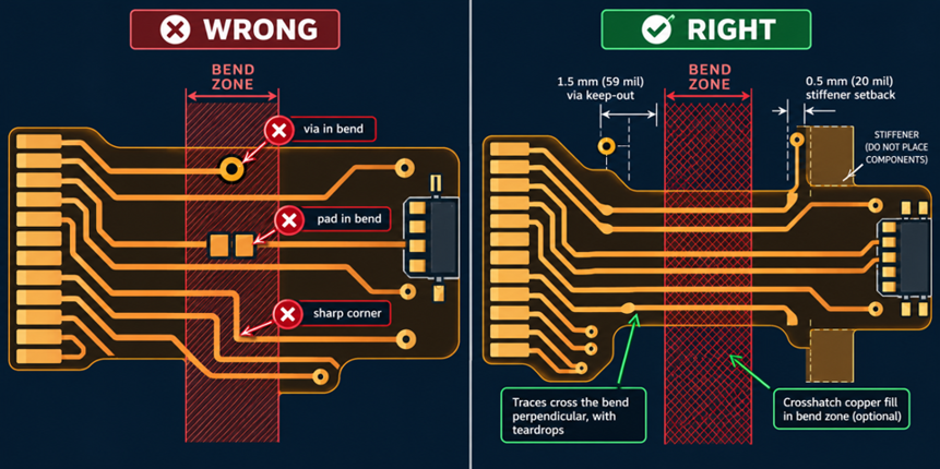
Figure 5: Bend-zone keep-out, with vias, pads, and stiffener edges held clear.
- Vias and plated holes: keep them at least 1.5 mm (59 mil) clear of the bend zone on both sides.
- Component pads and solder joints: keep them off the flexible section entirely, or back them with a stiffener.
- Stiffener edges: hold them 0.5 mm (20 mil) clear of where the bend begins, since the edge is itself a strain riser.
- Coverlay openings: keep them out of the bend, because an opening removes the layer that balances the stack.
Where a via has to sit close to a bend, teardrops spread the load into the surrounding copper. A hatched copper pour helps for the same reason, since a solid plane stiffens the flex and cracks in one piece.
Avoid Sharp Corners and Stress Concentration
Strain concentrates wherever a conductor changes direction or width abruptly. A 90-degree corner inside a bend zone is a crack waiting to start. Route traces across the bend perpendicular to the bend axis, and keep them straight through the flexible section. When a trace needs to turn, use a curved corner instead of a mitered corner. Make the corner radius at least three times the trace width. On a two-layer flex, stagger traces on opposite faces instead of stacking them, because overlapping copper behaves like one thicker conductor.
Consider Bend Cycles, Angle, and Installation Conditions
Cycle count separates two designs that look identical in the layout editor. A hinge rated for 10,000 cycles and one rated for a million need different copper and different radii. So that number belongs in the requirements before the stackup is chosen.
Bend angle matters less than most designers expect, since strain depends on radius rather than on arc length. Installation is the larger risk, because a circuit created by hand sees a radius close to zero. Your Gerbers describe the copper. The fab drawing describes the bend, and without one, no fabricator can check your radius.
How JLCPCB Supports Reliable Flex PCB Manufacturing
A calculated bend radius is only as good as the thickness the fabricator actually builds. T sits inside the multiplication, so process control through the bend zone keeps the calculation honest.
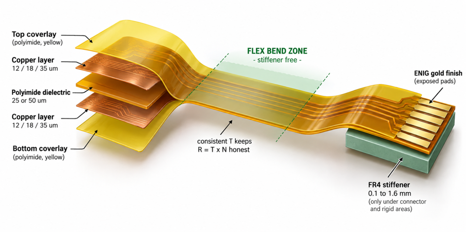
Figure 6: JLCPCB FPC stackup: copper, coverlay, stiffener, and the bend zone.
Precision FPC Manufacturing for Consistent Thickness and Layer Structures
JLCPCB builds flexible circuits in 1 to 4 layers on polyimide, with 25 µm and 50 µm dielectric options. Copper weights are available in 12 µm, 18 µm, and 35 µm sizes. Choosing the thinner dielectric and the lighter foil is the cheapest way to shrink a bend radius, because both feed straight into T.
Adhesiveless substrate and coverlay options keep the stack thin. Stiffeners are offered in polyimide (0.1 mm (4 mil) to 1.6 mm (63 mil)), FR4, and stainless steel. Placing one under the connector areas keeps the rigid parts rigid, so the flex bends only where you intended.
Flexible PCB Prototyping and Engineering Support
Flex prototypes are built in about 4 to 5 days with ENIG as the standard finish. So bending a real sample before committing to a mechanism costs very little. Physical testing catches the assembly crease that no calculation ever sees. Upload your Gerbers and fab drawing together on the JLCPCB quote page: Mark the bend area, the bend axis, and the minimum radius on the drawing. Engineering review then checks the built stack against what you specified, so a mismatch surfaces early.
Conclusion
Flex PCB bend radius reduces to one multiplication and one decision. Take the real thickness of the flexible section, multiply it by the ratio your bend type demands, then add a margin. Static bends forgive a tight radius, because the copper only has to survive one strain event. Foldable displays and wearables are pushing flex circuits toward tighter hinges and higher cycle counts. That favors single-layer, adhesiveless, rolled annealed builds. When your design is ready for hardware, JLCPCB's flexible PCB service covers 1- to 4-layer FPCs with the stiffener and coverlay options these builds require.

FAQs About Flex PCB Bend Radius
Q: Can I bend a flex PCB tighter than the minimum radius just once during assembly?
Ans: A single bend below the minimum often survives, but it leaves permanent damage in the copper. It shows up later as an intermittent open. If the mechanism forces it, move that section to single-layer construction rather than accepting the tighter bend.
Q: Is the bend radius measured to the inside or the outside of the curve?
Ans: Bend radius is measured to the inside surface of the flex, the face pressed against the mechanism. Measuring to the center of the stack gives a figure half a thickness too large, which matters on tight static bends.
Q: Can a stiffener protect the flex in a bend area?
Ans: A stiffener makes that section rigid, so it does not protect the bend at all. It moves the bend to the stiffener edge, concentrating strain there. Keep stiffener edges at least 0.5 mm (20 mil) back from where the bend begins.
Q: Why did my flex fail after a few thousand cycles when the radius met the static minimum?
Ans: Static minimums assume one strain event, so they are set by copper elongation rather than fatigue life. Repeated bending needs 100:1 for single-layer flex and 150:1 for double-layer. Rolled annealed copper is required as well.
Q: Does a larger bend radius hurt anything?
Ans: Electrically, no, and mechanically, yes, a larger radius always improves life. The only cost is space, because the flex needs a longer service loop and a wider curve in the enclosure.

Popular Articles
• Understanding the Basics of Electronic Devices and Circuits
• Understanding Digital Circuit Timing: Setup Time, Hold Time, Contamination Delay & Clock Skew
• PCBs Explained: A Simple Guide to Printed Circuit Boards
• Guide to the Top 10 Commonly Used Electronic Components
• Digital 101: Fundamental Building Blocks of Digital Logic Design
Keep Learning
Polyimide Flex PCB: A Complete Guide for Engineers
A polyimide flex PCB can be folded about 285,000 times when the base film is 25 µm (1 mil) thick. Make that film 75 µm (3 mil), and the same MIT fold test gives up near 6,000 cycles. Bending is a strain problem, not a material problem. Copper sits above the center of the stack, so a bend forces it to stretch around the longer outer path. Figure 1: A polyimide flex circuit folded tight, with a stiffener holding the connector A thicker stack places the copper farther out, resulting in more stretch at th......
Flex PCB Bend Radius: Calculation, Minimum Radius & Design Guidelines
Flex PCB bend radius is the one dimension on an FPC that no design rule check will catch. Bend the circuit tighter than its material allows; the outer copper stretches from its elongation limit, and then it cracks. Figure 1: A flex circuit formed around a mandrel, with bend radius and stack thickness A flex circuit bends around a neutral axis near the middle of its stack. Copper below that line is squeezed, and copper above it is pulled. So the further a layer sits from the line, the harder it is to w......
Flexible Circuit Connector: Types, Features & Selection Guide
A flexible circuit connector clamps onto the bare copper at the end of a flex circuit, so nothing is soldered at that joint. The tail slides into the housing, and an actuator presses a row of spring contacts onto the pads. Every connector is built around one tail thickness. TE's 0.5 mm pitch 2328702 family expects 0.30 mm (12 mil) of flex, because the contact beams are deflected by exactly that dimension. Figure 1: Cross-section of a 0.5 mm pitch FPC connector with the tail inserted Feed it a bare sin......
FPC vs FFC: Understanding the Key Differences Between Flexible Circuit Technologies
The FPC vs FFC decision is really a question about how the copper was made. An FFC consists of flat copper strips laminated between two PET films. Every conductor runs straight from end to end at one fixed pitch, because nothing in that process can make a trace turn or branch. An FPC starts as copper-clad polyimide and is etched exactly like a rigid board. Traces can turn, taper, split onto a second layer, and land under a soldered component. The finished circuit can be as thin as 0.1 mm (4 mil). Figu......
A Comprehensive Guide to Capacitor ESR: What It Is, Good Values, and How to Measure It
Key Takeaways Definition: Capacitor ESR (equivalent series resistance) is the single resistance that represents the losses inside a real capacitor, from its electrodes, terminations, electrolyte, and dielectric. Why It Matters: Ripple current flowing through the ESR produces a ripple-voltage step on the supply rail and I²R heating in the capacitor, which limits the capacitor's ripple-current rating and service life. Conditions Matter: ESR varies with frequency, temperature, capacitance, case size, and......
Understanding IPC-6012 Standards for High-Reliability Rigid PCB Fabrication
Key Takeaways IPC-6012 vs. IPC-A-600: IPC-6012 is the binding specification, while IPC-A-600 is only for visual reference. Class 2 vs. Class 3: Class 3 requires thicker copper (25μm vs. 20μm) and zero plating voids. Coupon Verification: Quality is tested by microsectioning panel coupons after thermal stress. Upfront Callout: Specify the class on drawings upfront; boards cannot be upgraded later. IPC-6012 is the line on your fabrication drawing that decides what your supplier is allowed to ship. Most d......