
Unlocking Smaller and Smarter PCBs with Embedded Components
12 min
- What Embedded Components Are and Why They Matter
- Critical Design Considerations
- The General Manufacturing Process
- Common Challenges and Industry Solutions
- Evolving Manufacturing Approaches: HDI vs. Advanced Multi-Layer
- Frequently Asked Questions (FAQ)
- Conclusion
Have you ever opened a smartwatch or a pair of wireless earbuds, looked at the miniature chip inside, and wondered how engineers could pack so much functionality into such a small enclosure? While surface-mount technology (SMT) has become incredibly sophisticated—with the advent of ultra-small 0201 and 01005 packages—there is a physical limit to how many components can be crammed onto the surface of a board. To bypass this bottleneck, the electronics manufacturing industry is increasingly turning to embedded components. Resistors, capacitors, and even bare silicon dies are now being mounted directly inside the internal layers of the PCB. Far from being a futuristic laboratory concept, this technology is actively transforming modern electronics.
By burying parts inside the board, designers can reclaim valuable surface area, drastically shorten signal paths, and eliminate delicate surface solder joints that consume space and introduce failure risks. This guide provides a comprehensive, educational overview of what embedded components are, how they are designed and manufactured, the challenges they present, and how the electronics manufacturing industry brings this technology to mass production.
Note
This article is intended solely for the purpose of introducing electronics industry development trends. JLCPCB does not currently support the advanced embedded component manufacturing and related HDI fabrication processes described in this article.
What Embedded Components Are and Why They Matter
Definition and Types of Embedded Components
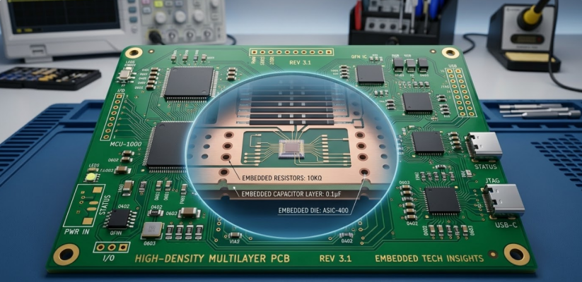
Embedded components are active or passive electronic elements placed within the inner layers of a PCB rather than soldered onto the outer surfaces. Instead of utilizing traditional surface solder pads, an embedded component is integrated directly into the laminate stack-up, with electrical connections established through vias and internal copper traces. The core standards governing this technology are IPC-6012E (qualification and performance of rigid PCBs) and IPC-2316 (design standard for embedded components).
The industry categorizes these components based on their materials and integration methods:
- Embedded Passives: Passive components rely on well-established material systems. For instance, embedded resistors are typically fabricated using thin-film nichrome (NiCr) or nickel-phosphorus (NiP) alloys deposited on copper foil, or carbon-based resistive foils like Ohmega-Ply. Embedded capacitors utilize thin, high-K dielectric layers embedded within the laminate stack-up.
- Bare Die Embedding: On the active side, bare silicon dies are thinned down to roughly 50–100 micrometers and inserted into precisely milled or laser-ablated cavities within the core or prepreg layers.
- Packaged IC Embedding: Alternatively, fabricators can embed ultra-small, pre-packaged integrated circuits (ICs), such as 0201, 01005, or wafer-level chip-scale packages (WLCSP) directly into the laminate.
| Component Type | Common Materials / Methods | Typical Tolerance / Spec | Primary Benefit |
| Embedded Resistor | NiCr thin-film, NiP, Ohmega-Ply carbon foil | +/-1% to +/-5% (laser trimmed) | 40-60% surface count reduction |
| Embedded Capacitor | 3M C-Ply, DuPont HK, BaTiO3-filled resin | pF to low nF range | Ultra-low ESL (10-50 pH) |
| Embedded Inductor | Spiral/meander PCB traces | Application-dependent | No discrete footprint needed |
| Embedded Bare Die | Thinned silicon (50-100 um) in cavity | Known-Good-Die required | Shortest possible interconnect |
| Embedded Packaged IC | 0201, 01005, WLCSP in laminate | Package-spec dependent | Eliminates solder joints |
Key Benefits for Size, Performance, and Reliability
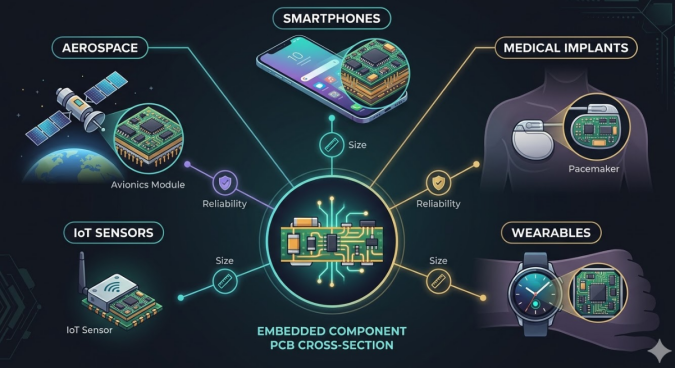
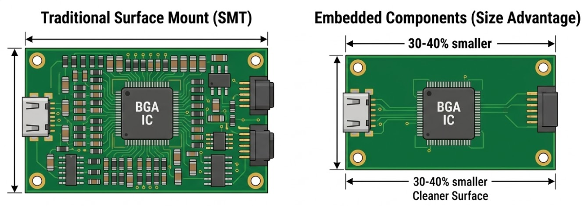
The most obvious driver for embedding components is miniaturization. Moving passive and active components off the outer layers typically yields a 20–40% savings in board area. For space-constrained applications like hearing aids, smartwatches, and IoT sensor nodes, this reclaimed real estate can be the deciding factor in whether a product fits into its intended chassis.
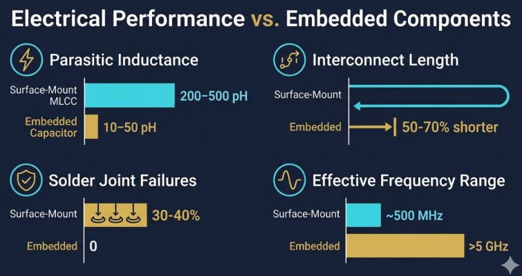
Electrical performance sees a massive boost due to shortened interconnects. The trace routing between an embedded decoupling capacitor and the power pin of a Ball Grid Array (BGA) can be shortened by 50–70% compared to a surface-mount equivalent. Shorter traces mean substantially lower parasitic inductance. Industry data indicates that solder joints are responsible for roughly 30–40% of assembly-level failures. Because embedded components are locked securely inside the laminated structure, they eliminate surface solder joints that would otherwise be prone to cracking under thermal cycling, heavy vibration, or mechanical shock.
Critical Design Considerations
Placement, Layer Integration, and Thermal Management
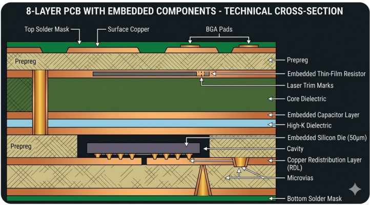
Integrating components into internal layers requires strict adherence to specialized design rules to ensure manufacturability. Internal components must be kept away from high-mechanical-stress zones, such as board edges, mounting holes, and heavy connector footprints. Cavity depth and component spacing must strictly match the fabricator's recommendations to ensure proper resin flow during lamination.
To prevent severe board warpage during the high-pressure lamination process, the PCB stack-up must remain perfectly symmetrical. Dedicated layers for embedded resistors or capacitor planes must be balanced evenly around the board's midplane.
Because embedded components lack direct airflow, heat must dissipate entirely through the surrounding laminate and copper. Designers mitigate this by placing dense thermal via arrays directly above and below power-consuming components to create a low-resistance path to external heat sinks. Additionally, filling adjacent layers with solid copper and utilizing high-conductivity prepregs (1 to 3 W/mK) helps distribute the thermal load.
Signal Integrity and Power Distribution Rules
From a Power Distribution Network (PDN) perspective, embedded capacitance planes provide excellent distributed decoupling across the entire board, far outperforming individual surface caps. However, designers must ensure reference planes remain continuous over component layers. High-speed traces should never cross straight over an internal cavity; the missing copper creates a discontinuity in the return path, causing severe impedance mismatch. Furthermore, an embedded capacitor's ultra-low Equivalent Series Inductance (ESL) of 10–50 picohenries provides effective broadband decoupling from 100 MHz up to several gigahertz—a performance tier that standard 0402 or 0201 SMT capacitors (with ESL values of 200–500+ pH) cannot replicate.
| Parameter | Embedded Capacitor | 0402 SMD MLCC | Improvement Factor |
| Equivalent Series Inductance (ESL) | 10-50 pH | 200-500+ pH | 5x to 50x lower |
| Effective Decoupling Range | 100 MHz to multi-GHz | Up to ~500 MHz | Broader bandwidth |
| Interconnect Path Length | Direct via connection | Pad-trace-via-plane | 50-70% shorter |
| Board Area Consumed | Zero (internal) | 0402: 1.0 x 0.5 mm pad area | 100% surface savings |
The General Manufacturing Process
Build-Up, Cavity Creation, and Component Embedding Steps
Manufacturing a PCB with internal components relies on a highly controlled, multi-stage sequential build-up process that demands tighter tolerances than standard multi-layer fabrication. A typical workflow follows these steps: Core Fab & Inner Imaging ➔ Cavity Creation ➔ Component Placement ➔ Lamination ➔ Via Formation ➔ Outer Layer Processing.
Note
The embedding of bare dies and Redistribution Layer (RDL) structures typically relies on the advanced HDI process route mentioned above.
- Core Fabrication and Inner Layer Imaging: Standard subtractive etching forms the internal copper patterns, including any specialty resistive-foil or capacitor plane layers.
- Cavity Creation: Pockets are precisely milled or laser-ablated into the core or prepreg layers to accommodate discrete components or dies. Mechanical milling systems routinely achieve an accuracy of ±25 micrometers.
- Component Placement: Ultra-precise pick-and-place machinery inserts components into the prepared cavities. Depending on the design architecture, components can be placed face-down (flip-chip style), face-up, or film-attached to a carrier layer before being pressed.
- Lamination: The entire layer stack-up is bound together in a vacuum press at 200 to 400 PSI and heated to temperatures between 180°C and 200°C, causing the prepreg resin to flow uniformly around the buried components.
- Via Formation : Precision mechanical drilling, controlled-depth drilling, or laser ablation is used to form vertical interconnects between the embedded component pads and the adjacent copper layers.
- Outer Layer Processing: The outer layers are subsequently imaged, etched, plated, and finished with standard processing line workflows.
Inspection and Quality Control
Because a buried component cannot be reworked or replaced after lamination, a "zero-defect" quality framework is mandatory. Advanced electronics fabricators maintain strict layer alignment tolerances—typically within ±25 micrometers for passives and 10 to 15 micrometers for bare dies.
To achieve this, automated optical inspection (AOI) and X-ray systems verify component placement and layer registration throughout production. Statistical Process Control (SPC) is monitored in real time—including lamination pressure, temperature profiles, and drilling accuracy. After lamination, high-precision LCR meters check component values, and laser trimming is applied if a resistor needs to hit an exact tolerance. Once fully assembled, boards undergo extensive flying-probe testing, industrial CT scanning to check for internal micro-voids, and Highly Accelerated Life Testing (HALT) to ensure long-term durability up to IPC Class 3 standards.
Common Challenges and Industry Solutions
Heat Dissipation and Reliability Issues
Despite its benefits, embedding components introduces notable manufacturing hurdles that must be managed. Standard FR-4 laminate is a poor thermal conductor, offering a thermal conductivity of only 0.25 to 0.35 W/mK. Internal components cannot dissipate heat via air convection like surface components can. Furthermore, a sharp Mismatch in the Coefficient of Thermal Expansion (CTE) between silicon (~2.6 ppm/°C) and FR-4 laminate (~14–17 ppm/°C) can cause internal stress during thermal cycles.
The rework dilemma is another key challenge: once a board is laminated, the embedded components are permanently sealed; if a single internal component fails or shifts out of alignment, the entire board must be scrapped.
How Advanced Manufacturing Overcomes These Challenges
To overcome these challenges, experienced manufacturers employ strategic workarounds. Thermal bottlenecks are mitigated by swapping standard materials for high-conductivity laminates (1 to 3 W/mK) or introducing integrated copper coins and thermal slugs that create a direct metallic conduit from the buried component to an external heatsink. These techniques can cut junction-to-board thermal resistance by 50% or more.
To counteract the lack of reworkability, the industry enforces rigorous pre-screening, such as requiring Known-Good-Die (KGD) testing for all active silicon chips prior to insertion, and maintaining a high Statistical Process Control capability index (Cpk > 1.33) across all critical manufacturing dimensions.
Evolving Manufacturing Approaches: HDI vs. Advanced Multi-Layer
Manufacturing Capabilities for Embedded Component Designs
As the demand for smaller, smarter electronics grows, the manufacturing strategies for embedded PCBs continue to diversify. The industry does not rely on a single approach; instead, fabricators match the process complexity to the specific requirements of the design.
For ultra-dense, high-tier integrations—such as embedding bare silicon dies with microscopic pin pitches—specialized high-density interconnect (HDI) manufacturing lines utilizing laser-drilled microvias (typically 75 to 150 micrometers), stacked filled-and-capped vias, and ultra-fine line widths remain a primary industrial pathway.
Integrated DFM Support and High-Yield Production
Conversely, for applications focused on embedding passive elements (like thin-film resistor foils and capacitor layers) or micro-packaged discrete components (such as 01005 or 0201 packages), manufacturers can successfully utilize high-precision, standard multi-layer PCB processes without full-scale HDI. By optimizing deep-controlled mechanical drilling, utilizing high-accuracy layer registration, and implementing real-time Statistical Process Control (SPC) over lamination pressures, temperature profiles, and drill accuracy, reliable connections can be established to components integrated within a standard multi-layer stack-up (supported up to 32 or more layers). This approach provides a highly reliable, accessible alternative for achieving the benefits of embedded components using robust, precision multi-layer workflows.

Frequently Asked Questions (FAQ)
Q1: What types of components can be embedded inside a PCB?
Both passive and active components can be embedded. On the passive side, resistors (using thin-film NiCr, NiP, or carbon-based foils like Ohmega-Ply), capacitors (using high-K dielectric materials like 3M C-Ply or barium titanate-filled resin), and inductors (as spiral or meander trace patterns) are all commonly embedded.
Q2: How do embedded components improve signal integrity in high-speed designs?
Embedded components dramatically reduce the interconnect path length between a decoupling capacitor and the power pin it serves, typically by 50 to 70 percent. This shorter path results in much lower parasitic inductance. An embedded decoupling capacitor can achieve an ESL of just 10 to 50 picohenries compared to 200 to 500 picohenries for a surface-mount 0402 MLCC.
Q3: What is the cost impact of embedded components vs. traditional surface-mount?
Embedded component PCBs have a higher per-board fabrication cost due to additional process steps, tighter tolerances, and specialized materials. However, the total system cost can be lower when you account for reduced board area (smaller and cheaper boards), fewer assembly steps (less pick-and-place time), elimination of discrete component procurement for embedded passives, and improved reliability that reduces warranty and field-failure costs.
Q4: What design software supports embedded component PCB design?
Several professional EDA platforms support embedded component definition and simulation. Cadence Allegro and Sigrity provide robust embedded component modeling and PDN analysis. Altium Designer supports embedded component placement within its unified design environment. Siemens Mentor Xpedition offers advanced embedded component workflows.
Conclusion
Embedded component technology represents a paradigm shift in modern electronics design, breaking through the physical real estate limits of traditional surface-mount technology. By transitioning from two-dimensional placement to a fully utilized three-dimensional internal layout, engineers can unlock unprecedented miniaturization, exceptional high-speed signal integrity, and superior mechanical reliability across diverse applications, from consumer wearables to robust automotive and aerospace systems.
While internal component lamination completely eliminates traditional surface rework loops, the key to successful, high-yield mass production lies in picking the right manufacturing strategy and executing seamless Design for Manufacturability (DFM). As manufacturing lines continue to bifurcate—offering specialized high-tier HDI paths for active bare dies alongside highly scalable, cost-effective precision multi-layer processes for passive element embedding—this once-exclusive technology is becoming highly accessible. By bridging the gap between rigorous design discipline and industry-standard fabrication controls, electronics innovators can confidently push past conventional boundaries and deliver next-generation, high-performance systems to the global market.
Keep Learning
Unlocking Smaller and Smarter PCBs with Embedded Components
Have you ever opened a smartwatch or a pair of wireless earbuds, looked at the miniature chip inside, and wondered how engineers could pack so much functionality into such a small enclosure? While surface-mount technology (SMT) has become incredibly sophisticated—with the advent of ultra-small 0201 and 01005 packages—there is a physical limit to how many components can be crammed onto the surface of a board. To bypass this bottleneck, the electronics manufacturing industry is increasingly turning to e......
Improving Heat Dissipation : The Smart Use of Thermal Pads in PCB Design
Key Takeaways Optimizing PCB thermal pad design and via arrays is essential to prevent semiconductor failures caused by FR4's low thermal conductivity. By implementing a 1.0–1.2 mm via pitch and keeping solder voiding below 25% through segmented stencils, designers can eliminate localized hot spots and boost board reliability from prototype to high-volume production. Have you ever considered that the thermal conductivity of a normal FR4 PCB is only about 0.3 W/mK? That is an acceptable number for low-......
Comparison of BGA vs LGA in High-Power Applications
Key Takeaways In high-power PCB designs, BGA and LGA packages offer strong high I/O performance but require effective thermal management. BGA excels with solder balls and thermal vias, while LGA relies on direct pad contact with TIMs and thermal pads. Key to success are thermal vias, thicker copper layers, ground planes, and simulations to reduce thermal resistance and maintain reliable junction temperatures. As electronic devices continue to shrink in size while increasing in performance, managing he......
A Complete Guide to IC Package: Types, Properties, PCB Design Rules & Selection Tips
What is an IC Package? An IC package is the physical enclosure that houses an integrated circuit or electronic component, providing mechanical protection, electrical connections, and thermal management. It ensures that the component can be reliably mounted on a PCB and integrated into circuits. Key Functions of an IC Package: 1. Mechanical protection: Shields the chip from physical damage and environmental factors. 2. Electrical connections: Provides pins or solder balls to connect the IC to the PCB. ......
BGA vs LGA: Understanding the Differences and Choosing the Right Package
In the world of electronic components, the choice of package type plays a crucial role in the overall performance, reliability, and manufacturability of a printed circuit board (PCB). Two popular package types that are widely used in modern PCB design are BGA (Ball Grid Array) and LGA (Land Grid Array). Understanding the differences between these two packages is instructive for electronics enthusiasts, hobbyists, engineers, students, and professionals in the field of electronics and PCB design. This a......
Technical Guidance: BGA Design Rules
With the advancement of the electronics industry, chip integration continues to increase, the number of IO pins quickly rises, and power consumption grows accordingly, leading to stricter requirements for integrated circuit packaging. To meet the demands of this progress, Ball Grid Array (BGA) packaging technology is introduced. This technology involves the creation of an array of solder balls on the bottom of the package substrate as the I/O interface for the circuit, connecting it to the printed cir......