An Inside Look at the Modern PCB Manufacturing Steps
15 min
- Foundation Phase: Preparing PCB Design and Inner Layers
- Core Structural Assembly: The PCB Lamination Stage
- Interconnect and Surface Finishing Protocols
- Final Validation: PCB Finishing and Testing Standards
- Why JLCPCB Delivers Unmatched Manufacturing Quality and Efficiency
- FAQ about PCB Manufacturing Process
- Conclusion
key takeaways
- Early Defect Trapping: CAM DFM and AOI catch inner-layer opens and shorts before lamination seals the board.
- DFM Prevention: Automated checks catch acid traps, copper slivers, and clearance shortfalls early.
- Reliable Interconnects: Chemical desmear clears resin smear from hole walls to prevent thermal failure.
- 100% Net Testing: Flying probe or bed-of-nails systems test every net for opens and shorts before packing.
- IPC Compliance: Final QA verifies annular rings and plating thickness against IPC-A-600 Class 2 or 3.
The PCB manufacturing steps you rarely see are often the ones that determine whether a board survives in the field. Between uploading the Gerbers and receiving the finished boards, a panel passes through multiple inspection and quality checks, and any one of them can stop production.
A defect that escapes one checkpoint may stay hidden until much later. An inner-layer open, a weak via barrel, or a damaged solder-mask dam might pass a basic bench test but fail after repeated thermal cycling in a real product. This guide follows the PCB manufacturing line as a series of quality gates. At each step, you will see what the gate checks, which defects it catches, what it misses, and what happens next when a production panel fails.
Foundation Phase: Preparing PCB Design and Inner Layers
Think of the factory line as a sequence of irreversible gates. Each panel moves forward without returning. Once the lamination press closes, every internal layer is sealed inside the board, permanently beyond reach.
| Stage | Gate Applied | What It Catches | On a Fail |
|---|---|---|---|
| CAM and DFM | Rule check against factory limits | Acid traps, slivers, thin annular rings | Order paused, query to you |
| Inner layer etch | AOI against the CAM image | Opens, shorts, nicks, pinholes | Shorts trimmed, open the core |
| Lamination | Press thermocouples, coupon tests | Undercure, voids, misregistration | Press book quarantined |
| Drilling | First article check, bit sensors | Wrong position or size, missing holes | Panel pulled before plating |
| Plating | Microsection of a border coupon | Thin or voided barrel copper | Lot held, plating line rebalanced |
| Solder mask | Registration, coverage, cure | Ink on pads, broken dams, soft mask | Stripped and redone, or scrap |
| Electrical test | 100 percent net test, every board | Any open or short, buried included | The board was scrapped; the fault goes upstream |
| Final QA | Visual check against IPC-A-600 | Scratches, finish defects, and bad legend | Rejected before packing |
Automated DFM Verification and Photolithography
Design for manufacturing verification checks your Gerber and drill files before the factory cuts a sheet of laminate. The software measures every feature against the factory's production limits, rather than relying only on the limits in your own design rule check.
Three defect classes account for most of what it flags:
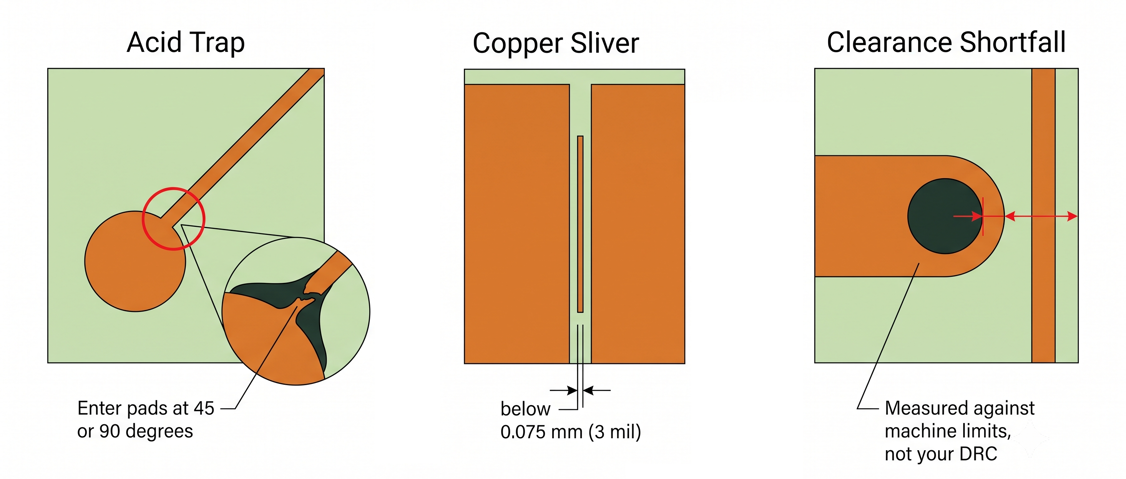
- Acid traps: When a trace enters a pad at less than 90 degrees, etchant pools in the sharp inside corner. It keeps working after the rest of the panel is clear, over-etching the corner into an open. Route into pads at 45 or 90 degrees.
- Copper slivers: A copper strip narrower than about 0.075 mm (3 mil) does not survive the etch tank. It breaks free, floats, and lands elsewhere on the panel as a short.
- Clearance shortfalls: Drill to copper, copper to outline, annular ring and mask dam width, each measured against what the machines actually hold.
Photolithography then defines the pattern. Dry film photoresist is heat laminated onto the copper, and light hardens it wherever copper should stay. The resist, not the light source, sets the resolution floor: conventional film resolves around 50 microns (2 mil), while laser-grade resist with direct imaging reaches about 25 microns (1 mil). Inner layers are imaged before lamination, the only moment their copper is reachable. Outer layers wait until after drilling, because the plated hole barrels belong to that same pattern.
Etching Inner Copper Tracks and AOI Inspection
Etching dissolves the copper left unprotected by the resist. Although the spray points downward, the chemical reaction also attacks exposed copper sideways beneath each resist edge. That sideways loss is called an undercut. It makes every finished trace trapezoidal rather than rectangular, with the top wider than the base. CAM compensates for this side loss.
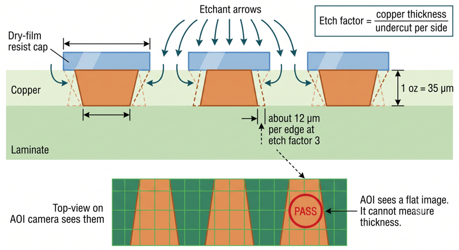
The etch factor is copper thickness divided by the undercut on one side. On inner layers, it runs between 2.5 and 4. On 1 oz copper, 35 microns (1.4 mil) thick, an etch factor of 3 removes about 12 microns (0.5 mil) per edge. Because etching narrows the copper, CAM widens each trace before imaging so its finished width matches the dimensions in your drawing. The next checkpoint is AOI, or automated optical inspection. A camera scans the etched panel, aligns it using the fiducials, and compares the board against the CAM data. It can catch opens, shorts, nicks, mouse bites, spurs, pinholes, and excess copper before the board moves on.
Core Structural Assembly: The PCB Lamination Stage
Lamination turns separate etched cores into one solid board. It is also the least reversible step on the line, so its gates prove conditions rather than inspect results.
Layer Alignment, Prepreg Interleaving, and Material Stackup
The stack is built from the middle outward: etched cores, prepreg sheets between them, copper foil on the outside. Prepreg is glass cloth infused with partly cured resin, so it melts, flows between layers, and then cures permanently. Resin-rich prepregs fill around heavy copper better, while heavier glass styles set the bulk dielectric more cheaply.
Alignment is the hard part. Every core has already moved before it reaches the stack, for two reasons:
- Etch shrink: Removing copper releases tension in the glass weave. A core with 90 percent copper on one side and 20 percent on the other shrinks unevenly.
- Press flow: Resin moving under pressure drags the layers slightly out of position.
Post-etch punching corrects the first shift. An optical machine measures where that core's tooling targets actually ended up, then punches new stack alignment holes at the measured positions rather than the drawn ones. X-ray alignment follows the press cycle, finding the buried inner layer targets and drilling the tooling holes at the true center of the stack, so the drill program references real copper rather than the panel edge.
High-Temperature Pressing and Bond Curing
The stack goes into a press that applies heat and pressure together under vacuum. A typical FR-4 cycle brings the laminate to around 185 C at 300 to 400 psi (roughly 20 to 28 bar) and holds it for 60 to 120 minutes before cooling under load.
The resin does three things in that window, in order. It softens and thins around 100 C to 120 C, flows to fill every gap between traces and push trapped air out, then gels and cross-links into a solid that can never be melted again. Bond curing is that third stage. The gates exist because you cannot see a cure; you can only measure it.
- Undercure leaves the resin only partly cured. Measured glass transition temperature comes out below spec, so the board softens earlier than it should and delaminates the first time it meets lead-free reflow at 245 C to 260 C.
- Overcure fails the other way. Held too hot or too long, the resin turns brittle, and excess flow squeezes dielectric out from between the layers. The board becomes too thin, shifting impedance away from your specified target.
Two checks catch these problems:
- Thermocouples: Probes inside the press stack measure the actual temperature of the panels. If the profile is out of range, the whole batch is held.
- Coupon testing: Test coupons are checked for Tg, cure level, and delamination after thermal stress.
If your board will go through multiple lead-free reflow cycles or rework, choose a high-Tg laminate from the start. A standard 130°C Tg material can be pushed beyond its limits during assembly.
Interconnect and Surface Finishing Protocols
Holes are what turn a stack of separate copper layers into one circuit. This phase exists to make a hole conduct reliably and to keep the pads solderable until they reach an oven.
Precision CNC Drilling and Hole Wall Copper Plating
Drilling is measured, not trusted. Before a run, the machine drills a first article panel that goes to an optical coordinate measuring machine, which checks hole position and diameter against the drill file. During the run, spindle load monitoring stops the machine the moment a bit snaps, so you lose one panel instead of two hundred boards missing the same hole.
Desmear comes next, though designers often overlook this hidden resin removal step during fabrication. Drilling heats the resin past its softening point, and the bit smears melted epoxy across the inner layer copper rings exposed inside the hole. Plate over that film, and the barrel sits on plastic instead of on the inner pad. The connection measures fine at room temperature and opens months later.
Desmear typically uses three baths: a solvent swells the resin, potassium permanganate removes it, and a neutralizer cleans the residue. With deeper treatment, etchback recesses the resin so roughly 12 µm (0.5 mil) of inner-layer copper extends into the hole, giving plated copper a stronger connection.
Applying Soldermask, Silkscreen, and Surface Finishes
Solder mask must align accurately, not merely cover the board. Its imaging process introduces its own separate registration error. Film-based imaging is typically around ±0.075–0.13 mm (3–5 mil), while direct imaging can be closer to ±0.05 mm (2 mil). That is why mask openings are usually made slightly larger than the pad. The thin strip between two mask openings is the dam. Below about 0.10 mm (4 mil), it can break during development and end up on another pad. JLCPCB supports 0.10 mm dams for 1 oz copper in standard mask colors.
Three checks cover this stage:
- Registration: Checks that mask openings are aligned and dams are intact.
- Cure: Confirms the mask is properly cured and will not lift during assembly.
- Thickness: X-ray fluorescence checks coating thickness without damaging the board.
A separate coupon test dips the finish into molten solder to verify solderability. A finish can look perfect yet solder poorly when incomplete cleaning leaves hidden contamination behind.
Final Validation: PCB Finishing and Testing Standards
Everything up to here has been checked in pieces, layer by layer, and bath by bath. The last two gates judge the board as a finished product, first electrically and then by eye.
Automated Flying Probe and Bed-of-Nails Electrical Testing
Electrical test sits near the end of the line, once the surface finish is on and before anything is packed. The board is complete by then, so the test proves what you will actually receive. It is a 100 percent test, not a sample. Every net on every board gets two separate checks: continuity along the complete path to rule out an open, then isolation from every other net to rule out a short circuit. Prototype quantities use movable probes and production quantities use a fixture, but the pass criteria are identical. What a failure triggers depends on how many boards fail and where:
- One board, one net: The board is scrapped. A bare board with an open trace inside the laminate cannot be repaired.
- Several boards, the same net: That points at the design, usually a feature sitting on the edge of capability, and it goes back to CAM.
- Several panels, the same location: The pattern indicates a process fault and identifies one machine: a scratched imaging drum, a blocked developer nozzle, or a drill beyond its hit count.
The third case is why the failure data is worth more than the failed board.
Final Contour Milling and Visual Quality Assurance
Contour milling cuts the finished board from the production panel. A router bit, often around 2.0 mm (79 mil), follows the outline while small tabs keep the board attached until the final pass. The outline is typically held to about ±0.2 mm (8 mil). Keep copper at least 0.3 mm (12 mil) away from the edge so the router does not expose or damage it.
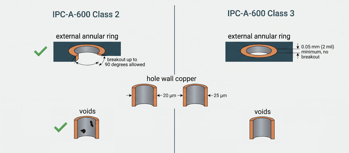
Then a person looks at every board, judging it against IPC-A-600. The class you ordered changes what passes.
| Acceptance Item | IPC Class 2 Allows | IPC Class 3 Requires | What It Means for Your Board |
|---|---|---|---|
| External annular ring | Breakout up to 90 degrees | No breakout, 0.05 mm (2 mil) ring minimum | Wider pads or tighter drill registration |
| Internal annular ring | Breakout up to 90 degrees | 0.025 mm (1 mil) ring minimum | Buried pads must be captured, not just touched |
| Average hole wall copper | 20 microns (0.0008 inch) | 25 microns (0.001 inch) | A thicker barrel survives more thermal cycles |
| Voids in the hollow wall | Limited voids accepted | No voids in the barrel | Plating line control becomes the gating cost |
Class 2 covers most commercial hardware. Class 3 is for boards where a field failure is not an inconvenience: an automotive ECU in a hot engine bay, an infusion pump, an avionics module.
Why JLCPCB Delivers Unmatched Manufacturing Quality and Efficiency
Every gate above only means something if it behaves the same way on panel 40,000 as it did on panel one. That consistency is a machinery and data problem rather than a skill problem.
Fully Automated Smart Factories with Industry-Leading Turnarounds
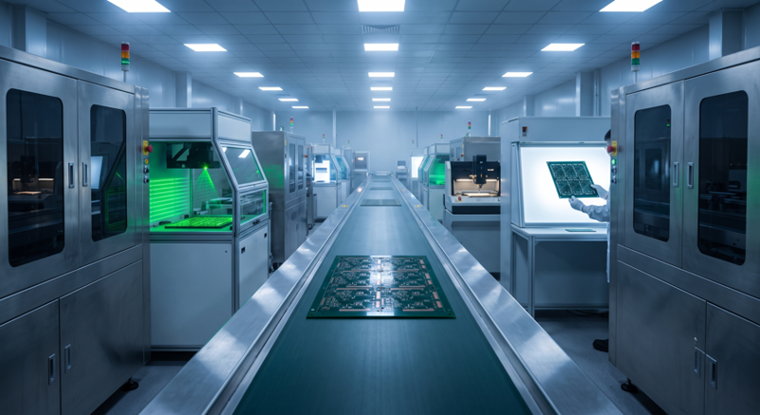
Repeatability comes from removing human variation from the line. JLCPCB runs fully automatic laser direct imaging, solder mask, etching, screen printing, and electroplating lines across a site of more than 320 acres, producing over 8 million square meters of PCB per year as of December 2025. Automation creates that speed without eliminating any required production steps. Standard fabrication finishes in as little as 24 hours, and orders with standard parameters paid before 6 pm GMT+8 enter production the same day.
The published capabilities tell you where the standard line ends:
- 1 to 32 layers on rigid FR-4
- 0.09 / 0.09 mm (3.5 / 3.5 mil) minimum trace and space on multilayer boards
- 0.15 mm (6 mil) minimum drilled hole on two layers and above
- 0.10 mm (4 mil) minimum solder mask dam at 1 oz copper
- Controlled impedance within plus or minus 10 percent, tightening to 5 percent on request
Designs within these limits move through at standard cost and lead time. The instant quote page flags out-of-spec features before you submit and pay for the order.
End-to-End Quality Traceability and Cost-Effective Production
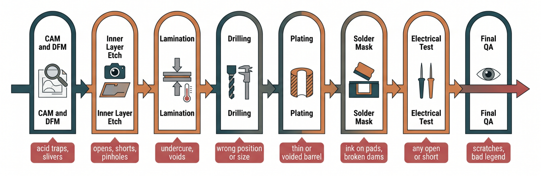
Traceability allows each quality problem to be diagnosed and corrected. The results from each of the inspection steps are noted on the panel, so that if a defect is discovered later, it can be traced back to the machine, shift, and operator involved. Materials are also monitored, and not just a generic FR-4 board is recorded, specifically the laminate and solder mask. Key checks are performed at three points – AOI after pattern plating, electrical testing of the completed board, and final visual testing before the board is packed. This directly affects cost: it will cost much less to locate a defect when it occurs in the production process than once the board is completed. One reason for the affordability of quick-turn PCB production is that.
FAQ about PCB Manufacturing Process
Q: How many steps are there in the PCB manufacturing process?
A rigid multilayer board goes through roughly 20 production operations, from CAM preparation to final packing. About eight of those are inspection gates rather than production steps, and they decide whether the panel keeps moving.
Q: At which PCB manufacturing step is a defect still repairable?
Inner layer copper can be touched up right until lamination, and solder mask can be stripped and reapplied. After the press closes, buried copper is unreachable, so defects found later usually mean the board is scrapped.
Q: What does AOI check that the electrical test does not?
AOI compares the etched copper against the CAM image, so it catches nicks, spurs, pinholes, and near opens that still conduct today. Electrical test only reports pass or fail on a net, so a trace etched down to a thread will pass it.
Q:Why is desmear needed before hole plating?
Drilling melts resin and smears it across the inner layer of copper exposed inside the hole. Plating over that film bonds copper to plastic instead of to the pad, giving a connection that works cold and opens after thermal cycling.
Q: What is the difference between IPC Class 2 and Class 3 at final inspection?
Class 3 removes allowances rather than adding tests. It forbids annular ring breakout, requires 25 microns of average hole wall copper against 20 microns for Class 2, and accepts no voids in the barrel.
Conclusion
Manufacturing steps for PCBs can be listed easily,y but it is hard to control them. Copper is imaged, etched, pressed, drilled, plated, masked, and cut and each of those operations has a tolerance that can vary by 10 microns or more before anyone on the shop floor would notice. It's the inspection that follows each step that ensures that your completed board is protected—and one concept underlies all of them: reachability.
The inner layer can be remounted until the press is closed. There's no better way to determine if a hollow wall than by cutting a sample in half. The only way to be sure of a buried connection is to have current. Working around those boundaries and gates can become valuable, predictable points. Now your copper, clearances off the capability floor, name your IPC class, the panel walks the line without a question.

Keep Learning
Understanding SMT PCB Boards Technology: An Essential Component of Modern Electronics
Surface Mount Technology (SMT) has changed manufacturing of modern electronics. It has made designs and assembly methods more efficient. Many modern electronics depend on SMT PCB boards, which make it possible for circuit designs to be small and efficient. This is what today's technology needs. This article discuss about many types of SMT PCB boards, their uses, and the best methods for designing and assembling them. 1. What is an SMT PCB Board? Printed circuit boards called SMT PCB boards, use surfac......
How to Choose the Right Prepreg Material for Reliable Multilayer PCB
Have you ever wondered what makes all those copper layers stick to a cross-section of a multilayer PCB? Prepreg material is the answer, and it is of much more importance than most engineers think it is. Choose the prepreg selection wrong, and you are predetermined to delamination, impedance drift, and long-term reliability problems. Prepreg is not only glue. It is a designed composite that determines your dielectric separation, dictates your impedance, affects signal loss, and determines your board be......
Via Filling Explained: Key Techniques, Benefits, and Solutions for High-Performance PCBs
Key Takeaways Via filling completely fills plated through-holes and microvias with epoxy or conductive copper paste, followed by planarization and copper capping (POFV). It eliminates voids, solder wicking, and thermal/mechanical issues while enabling reliable via-in-pad designs. Benefits include superior heat dissipation (up to 8 W/m·K), better signal integrity, higher mechanical strength, and improved assembly yields. JLCPCB provides free non-conductive filling + POFV on 6+ layer boards. Ideal for H......
How Fiducial Markers Guarantee Perfect Alignment in Professional PCB Fabrication
Today, the most sophisticated pick-and-place machine can place a 0.5 mm pitch QFP on its footprint, board after board, thousands of times, and never miss. It is not only a matter of expensive cameras or high-quality servos, but it begins with a little, very small copper dot, simply hanging there in the corner of your PCB. That dot represents a fiducial marker, and without it, even the smoothest SMT line would be laying components in the dark. The unrecognized heroes of automated assembly are the fiduc......
Technical Guidance: Character Design Specifications
To facilitate component assembly, future maintenance, and traceability of PCB manufacturing information (such as manufacturer, production date, batch number, etc.), various character markings are typically silk-screened onto the PCB. These include component designators, polarity marks, test point labels, company logos, and production traceability information. Traditional PCB character silk-screening uses the screen printing process, hence the term “silk-screen characters.” High-definition characters a......
Step-by-Step Guide to the Printed Circuit Board Manufacturing Process
Key Takeaways Core Role: PCBs provide the physical foundation and electrical connections for modern electronics. Multi-Step Process: Manufacturing spans design imaging, substrate creation, inner/outer layer etching, lamination, and surface finishing. Precision & Quality Control: Features micro-drilling (down to 100 µm) for layer connectivity, Automated Optical Inspection (AOI), and final electrical testing. Protection & Finish: Solder masks and surface finishes (e.g., ENIG, HASL) protect copper traces......