
How Copper Thieving Balances Your PCB for Better Manufacturing Results
10 min
- Introduction for Copper Thieving
- Why Copper Thieving Is Essential in Modern PCB Design
- Key Benefits for Reliable PCB Production
- Best Practices for Effective Copper Thieving
- Manufacturing Advantages of Professional Copper Thieving
- JLCPCB's Expertise in Copper Thieving Implementation
- FAQs about Copper Thieving
Key Takeaways
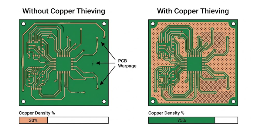
Copper thieving adds non-functional copper patterns (dots, squares, or crosshatch) to balance copper density across PCB layers. This effectively reduces uneven plating (from 20-30% to <10%), board warpage, inconsistent etching, and impedance issues, delivering tighter tolerances, better solder mask adhesion, higher yields, and lower costs. For best results, target 40-60% copper density per layer, maintain proper clearances, and ensure stackup symmetry. When done right, it transforms complex high-density PCBs into reliable, flat boards for superior manufacturing performance.
Introduction for Copper Thieving
Did you ever see tiny dots, squares, or crosshatch designs on blank spaces on a bare PCB? It is copper thieving in action, and it is one of the most effective and yet ignored techniques of providing uniform PCB manufacturing. Without it, your boards may be unevenly etched, plated, and warped, making what is a great design a production nightmare. The PCBs of modern times are more functional and can fit more into smaller areas, but this can leave large spaces of bare laminate directly adjacent to dense copper areas. This imbalance is a genuine issue when fabrication is done, since there is a variation in copper thickness and bow and twist, which may not meet IPC-6012 requirements. Copper thieving addresses this by adding non-functional copper patterns strategically to balance out distribution over your board.
We are going to discuss today what copper thievery is, why it is important, and how to make it work. Be it a 2-layer board or a complicated multilayer stackup, this technique is going to make your design yield better and save you the cost of unnecessary rework.
Why Copper Thieving Is Essential in Modern PCB Design
As circuit complexity grows, the copper distribution across a PCB layer becomes increasingly uneven. One corner might have a dense ground plane while the opposite corner has only a few isolated traces. This imbalance is exactly where copper thieving steps in.
What Copper Thieving Is and How It Works
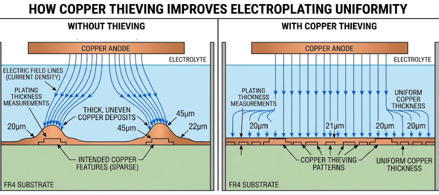
Copper thieving refers to adding non-functional copper features to sparsely populated areas of a PCB layer. These features, commonly called copper thieves, are not connected to any electrical network. They exist purely to equalize copper density across the board surface. The concept works on a simple principle. During electroplating, electric current flows preferentially toward isolated copper features, causing them to plate thicker than areas surrounded by dense copper. By adding copper thieves to empty regions, you redistribute the current density more evenly, resulting in uniform copper thickness.
Copper thieves come in several standard patterns:
- Dot patterns: Small circular pads in a grid, typically 20-40 mil diameter
- Square patterns: Small square pads in a regular array, common in aerospace boards
- Crosshatch patterns: A mesh of thin copper lines, balancing fill density and thermal management
- Solid fills: Complete copper pours in unused areas, providing maximum balancing but requiring careful clearance management
Common Problems It Solves in High-Density Boards
Without copper thieving, several manufacturing defects become significantly more likely. Uneven plating thickness is the most direct consequence, with variations of 20-30% or more across a single panel, violating IPC-6012 Class 2 and Class 3 requirements.
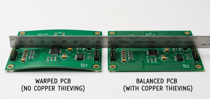
Board warpage is another major concern. When one side of a PCB has significantly more copper than the other, differential thermal expansion during reflow causes bow and twist. IPC-6012 limits this to 0.75% for surface mount boards, and copper imbalance is a leading cause of exceeding that limit.
Additional problems that copper thieving addresses include:
- Inconsistent etching rates leading to over-etched or under-etched traces
- Poor solder mask adhesion at abrupt copper-to-laminate transitions
- Delamination risk from uneven internal stress
- Impedance variations due to copper thickness inconsistencies
Key Benefits for Reliable PCB Production
Improved Etching Uniformity and Reduced Warpage
In the etching process, the copper is removed at various rates depending on the local copper density by the etchant. Thick areas are etched more slowly, and thin ones are etched faster. The resulting traces are broader in densely populated regions and narrower in sparsely populated ones. Equalizing density with copper thieves allows the etching rate to be uniform, allowing tighter trace width tolerances.
It is also important that warpage is minimized. Take the case of a 4-layer board with Layer 1 being filled with 80% copper and Layer 4 with 20%. Copper (CTE 17 ppm/C) and FR4 (CTE 12-16 ppm/C) have varying rates of expansion during reflow at 245-260 degrees Celsius. This differential stress is reduced by balancing copper on either side.
| Parameter | Without Copper Thieving | With Copper Thieving |
|---|---|---|
| Plating Thickness Variation | 20-30% across panel | Less than 10% |
| Trace Width Tolerance | +/- 1.5-2.0 mil | +/- 0.5-1.0 mil |
| Board Warpage (Typical) | 1.0-1.5% bow/twist | Less than 0.5% |
| Etching Uniformity | Inconsistent across zones | Uniform across panel |
| Solder Mask Adhesion | Variable | Consistent |
Higher Yield and Lower Manufacturing Costs
When copper distribution is unbalanced, fabricators compensate with tighter process controls, slower etching speeds, and additional inspection. All of these add cost and reduce throughput.
With proper copper balancing, first-pass yield improves significantly. Fewer boards get rejected for plating violations, trace width non-conformance, or warpage. Even a 2-3% yield improvement translates into meaningful cost savings at production volumes.
Best Practices for Effective Copper Thieving
Getting the most from copper thieving requires following established guidelines. Random placement can actually introduce new problems if not done carefully.
Placement Strategies and Density Balancing Rules
Most manufacturers target a copper density variation of less than 15-20% between the densest and sparsest regions. Here is a systematic approach:
1.Calculate the existing copper density for each layer using your EDA tool. EasyEDA and KiCad can report this automatically.
2.Identify sparse regions where copper density falls significantly below the layer average.
3.Choose the appropriate pattern. Dot patterns with 20-30 mil pads on 50-80 mil pitch work well for most applications.
4.Maintain proper clearance of 10-20 mil minimum between copper thieves and functional copper.
5.Balance inner layers too, not just outer layers. Unbalanced inner layers cause just as much warpage.
6.Ensure symmetry across the stackup. If Layer 1 has 70% copper density, the bottom layer should match. Pair the inner layers symmetrically about the board's center axis.
A useful rule of thumb is to target 40-60% copper density on each layer after thieving. This range balances manufacturing uniformity against excessive copper that could complicate routing.
Avoiding Common Design Mistakes
Placing thieves too close to impedance-controlled traces is the most frequent error. Always maintain at least 3W spacing (three times the trace width) between copper thieves and impedance-critical signals. Using solid fills instead of patterned thieves on signal layers introduces unintended capacitive coupling. Solid pours act as parasitic ground planes on high-speed lines. Patterned thieves reduce this risk substantially.
Other common mistakes include:
- Forgetting to add thieves to the inner layers, only balancing the outer layers
- Not accounting for copper thieves in DRC settings, leading to false violations
- Placing copper thieves within pad clearance zones, risking solder bridging
- Neglecting to coordinate with the fabricator about their thieving preferences
- Creating asymmetric copper distribution across the stackup centerline
Manufacturing Advantages of Professional Copper Thieving
When copper thieving is executed properly, the benefits extend throughout fabrication and assembly, transforming a problematic board into one that flows smoothly through every manufacturing step.
Enhanced Process Control and Consistency
From the fabricator's perspective, copper-balanced panels are significantly easier to process. The electroplating bath operates predictably because current distribution is uniform, allowing standard plating parameters without zone-by-zone adjustments.
During etching, balanced density lets the fabricator optimize spray pressure, temperature, and conveyor speed for a single condition rather than compromising between zones. The drilling process also benefits, as balanced copper ensures more uniform lamination pressure and better drill-to-copper registration.
Seamless Integration with Fabrication and Assembly
Copper thieving carries benefits into the assembly process. A flat, warp-free board sits properly in pick-and-place fixtures, ensuring accurate placement for fine-pitch components like 0.4mm pitch BGAs and 0201 passives.
| Manufacturing Stage | Impact of Copper Thieving |
|---|---|
| Lamination | Uniform pressure distribution, better layer registration |
| Electroplating | Even copper deposition, consistent plating thickness |
| Etching | Uniform etch rate, tighter trace width control |
| Drilling | Improved drill-to-copper registration accuracy |
| SMT Assembly | Better pick-and-place accuracy on flat boards |
| Reflow Soldering | Uniform thermal profile across the assembly |
During reflow, a flat board ensures consistent contact with conveyor rails, preventing temperature variations that cause cold joints or tombstoning. For wave soldering, even slight warpage causes inconsistent solder wave contact.
JLCPCB's Expertise in Copper Thieving Implementation
Choosing the right manufacturing partner matters for copper balancing. A fabricator that integrates copper thieving into their DFM process catches issues before they reach the production floor.
Advanced DFM Support for Optimal Copper Balancing
JLCPCB's engineering team reviews incoming designs through automated DFM analysis, which includes copper density evaluation across all layers. If your design has a significant imbalance, their team flags it during order review, giving you the chance to optimize before production begins.
Their system evaluates copper distribution at the panel level, not just at the individual board level. This matters because panelization can help or hurt copper balance depending on board arrangement. For EasyEDA users, the integration lets you check copper fill percentages directly in the design tool.
Precision Manufacturing Ensuring High-Quality Results
JLCPCB's fabrication facilities use tightly controlled electroplating processes that complement proper copper thieving. When your design provides balanced copper, their process delivers excellent thickness uniformity.
With production starting at $2 for standard PCBs and turnaround as fast as 1-2 days, iterating on copper balancing strategies is practical and affordable. Their surface finish options, including HASL, ENIG, OSP, and immersion silver, all benefit from the uniform copper surface that proper thieving provides.
Scalable Solutions from Prototype to Volume Production
Your copper thieving strategy stays consistent from prototype through volume production at JLCPCB. The same DFM checks apply whether you order 5 boards or 5,000. For volume orders, their SMT assembly services extend the benefits further, as flat boards improve pick-and-place accuracy and reflow consistency.
If you are looking to put these principles into practice, JLCPCB's instant quoting system lets you upload Gerber files and get immediate feedback alongside engineering support for DFM optimization.
FAQs about Copper Thieving
Q: What is copper thieving?
Copper thieving is the addition of non-functional copper patterns (dots, squares, or crosshatch) in sparsely populated areas of a PCB to balance copper density across the board.
Q: Why is copper thieving important?
It prevents uneven plating, board warpage, inconsistent etching, and impedance variations, ensuring the PCB meets IPC standards and achieves higher manufacturing yield.
Q: How does copper thieving work?
By adding extra copper in low-density areas, it equalizes current distribution during electroplating and etching, resulting in uniform copper thickness and reduced manufacturing defects.
Q: What copper density should I target?
Aim for 40-60% copper density per layer after adding thieves, while keeping density variation under 15-20% across the board.
Q: What are the key best practices for copper thieving?
Maintain 10-20 mil clearance from functional copper, ensure stackup symmetry, avoid placing thieves near impedance-controlled traces, and always coordinate with your PCB fabricator.
Popular Articles
Keep Learning
How to Design Your Own Keyboard PCB: From Layout to Firmware
Designing a custom keyboard PCB is one of the most rewarding entry points into practical electronics. You not only get a really useful product on your desk, but also you learn schematic capture, matrix scanning, footprint selection, USB, and firmware. Most of the hardware engineers use the same skills that show up on professional boards. This guide walks the entire build from choosing switches, wiring the diode matrix, adding the microcontroller and USB-C, laying out the board, and flashing QMK or VIA......
Don't Let Design Errors Ruin Your Hardware: The Complete Guide to PCB Design Verification
Key Takeaways PCB design verification is the systematic process of validating layouts against electrical, signal integrity, and manufacturing rules before production, preventing costly board respins and launch delays. Schematic verification through Electrical Rules Check (ERC) catches floating inputs, power shorts, and footprint mismatches before layout begins. Design Rule Checking (DRC) ensures trace widths, clearances, and via sizes comply with your fabricator's manufacturing tolerances, especially ......
How to Determine the Right PCB Voltage Clearance for Safe and Reliable Designs
Key Takeaways Clearance is the air gap; Creepage is the surface path — both essential for high-voltage safety. Base spacing on peak voltage and follow IPC-2221 / IEC 60664-1 standards. Major factors: voltage, pollution degree, CTI, altitude, and conductor location. Use isolation slots, guard rings, and conformal coating to optimize spacing. Always run clearance calculations, DFM checks, and Hipot testing before production. Why do two copper traces that work fine at 5V suddenly arc over and burn at 400......
Mastering PCB Footprints: Design Best Practices for Reliable Manufacturing
Key Takeaways A PCB footprint (land pattern) translates component datasheet dimensions into copper pads, solder mask openings, paste apertures, silkscreen, and clearance areas that enable reliable soldering and assembly. Follow IPC-7351 standards and manufacturer DFM rules for pad dimensions, spacing, and layer design to minimize defects like solder bridging, tombstoning, and cracked joints. Choose between through-hole (THT) and surface mount (SMT) footprints based on electrical needs, thermal perform......
How Copper Thieving Balances Your PCB for Better Manufacturing Results
Key Takeaways Copper thieving adds non-functional copper patterns (dots, squares, or crosshatch) to balance copper density across PCB layers. This effectively reduces uneven plating (from 20-30% to <10%), board warpage, inconsistent etching, and impedance issues, delivering tighter tolerances, better solder mask adhesion, higher yields, and lower costs. For best results, target 40-60% copper density per layer, maintain proper clearances, and ensure stackup symmetry. When done right, it transforms comp......
ZIF Connectors Simplify Flexible PCB Assembly with Tool-Free Reliability
Did you ever attempt to mate a fragile flex cable into a connector and experience that unpleasant resistance, and wonder whether you were tearing off the tail or breaking the casing? It is precisely that tension that the ZIF connectors were supposed to help remove. Zero insertion force technology allows you to slide a flexible printed circuit or flat flexible cable into the receptacle to be mated with, using almost no push force at all, but rather allows a mechanical actuator to hold the cable firmly ......