How Edge Plating PCB Improves EMI Shielding & Design Rules for Manufacturing
16 min
- What is PCB Edge Plating and Why Do Engineers Use It?
- Common Applications and Different Treatments for PCB Edge Plating
- Step-by-Step Breakdown: The PCB Edge Plating Process
- Essential Design Guidelines for Successful Edge Plating
- Why JLCPCB is Your Trusted Partner for Reliable Edge Plating
- FAQ about pcb edge plating
- Conclusion
Key Takeaways
- EMI Shielding: Seals board edges with copper to cut radiation and lower ground inductance.
- 4 Plating Types: Supports Full, Selective, Castellated, or Slot plating depending on layout needs.
- Keep-Out Rules: Pull back non-ground traces 0.5 mm to prevent short circuits from edge wrap.
- Manufacturing Limits: Requires tab-routing with 3+ gaps instead of V-scoring, and uses ENIG finish.
PCB edge plating is a process that surrounds the outer wall of the PCB with copper. A bare fiberglass edge is converted into a grounded metal skin. Reduces radiated emissions and allows a board to be soldered directly into a metal enclosure. It also has a current that an ordinary trace could not take.
In this guide, you will learn:
- What edge plating PCB is and how it shields EMI
- The four different treatments for PCB edge plating
- Every stage of the PCB edge plating process
- Clearance and keep-out values that prevent shorts
- How to panelize a plated board with breakaway tabs
- Capability limits, surface finish, and cost drivers
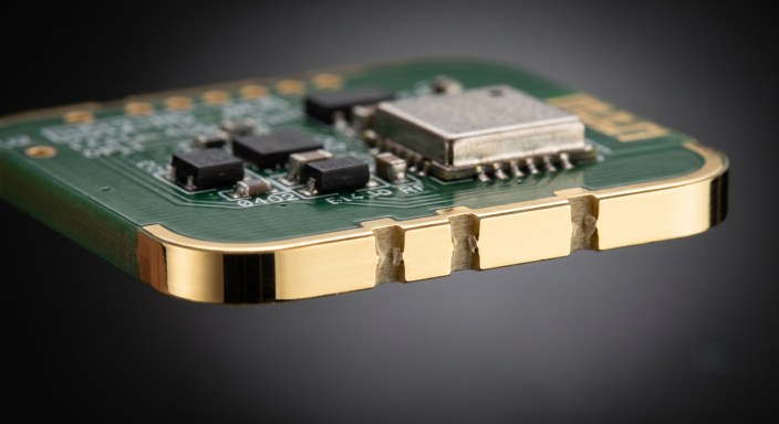
Figure 1: A four-layer PCB with fully plated
What is PCB Edge Plating and Why Do Engineers Use It?
Defining Edge Plating PCB and Its Core Purpose
PCB edge plating is a layer of copper deposited on the vertical side wall of a board. It runs continuously from the top copper layer, down the routed edge, to the bottom copper layer. Fabricators also call it side plating, plated edge, or wrap plating. The finished perimeter conducts, so it no longer exposes bare glass and cured resin.
A plated edge does the opposite, and forces the copper right up to the profile, so the fabricator has something to wrap onto. This one option affects the outline, pours, and solder mask drawing. Edge plating is thus not only an ordering checkbox, but also a design decision.
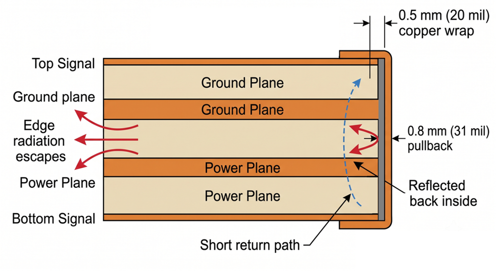
Figure 2: How a plated edge closes the radiating gap between two ground planes
Key Electrical and Mechanical Benefits
A pair of ground planes joined by a plated edge forms a conductive box. Five of its six sides are closed, which makes the board a partial Faraday cage. Energy that would have radiated out of the open edge now meets a continuous conductor. It turns into surface current and returns to ground instead. A board-level shield can be soldered to that same ground, closing the sixth side.
A single wire or screw boss bonds the board to a metal chassis at one point. At 2.4 GHz, even 10 mm (394 mil) of wire has enough inductance to look like an open circuit. A plated edge clamped along its full length gives continuous contact instead. The bond inductance collapses, so the ground reference stays flat across frequency. Current capacity is the benefit that gets overlooked. Plate 25 microns (1 mil) of copper up a 1.6 mm (63 mil) board wall. That gives roughly 0.04 mm squared of copper cross-section. A 1.1 mm (43 mil) trace in 1 oz foil has exactly the same metal area. Plated edges, therefore, appear on motor drives and battery packs, where a ground return is required.
Common Applications and Different Treatments for PCB Edge Plating
Ideal Use Cases for Metalized Edges
Radio modules are the largest single market for plated edges, and you already own several. A smart speaker holds a Wi-Fi module, and a fitness tracker holds a Bluetooth one. Both are small PCBs reflowed onto a larger carrier board through plated features on the perimeter. That perimeter carries the connections and the ground seal for the metal can on top. Boards that slide into an extruded aluminum housing are the second common case. An industrial sensor rarely has room for a shield can, so the housing itself becomes the shield. The board edge is then how you bond to it. Plating the two long edges lets spring fingers press against solid copper rather than laminate. Bond resistance stays under a milliohm for the life of the product.
Several other designs reach for the feature for narrower reasons. None of them needs a full shield, but all of them need metal where laminate would normally be:
- High current returns on motor controllers and battery packs, where the plated edge doubles as a ground busbar.
- Heat spreads on the LED and power boards, since the copper wall conducts heat sideways into a clamped chassis.
- Edge soldering of daughterboards into a slot, where the board is soldered on its side instead of through pads.
- Handling durability on connector edges and test coupons that get gripped and removed thousands of times.
Different Treatments for PCB Edge Plating Across Diverse Designs
Four treatments cover almost every plated edge you will order. They differ in how much of the wall gets metalized, not in the chemistry behind it. The choice comes down to what the edge actually has to do. You need either a continuous shield, a set of solder connections, or one grounded strip.
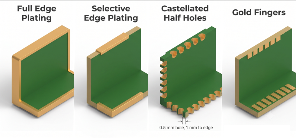
Figure 3: The four edge plating treatments compared side by side
| Treatment | What Gets Plated | Typical Use | What to Watch |
|---|---|---|---|
| Full edge plating | All four sides except the 3 to 4 tab breaks | Shielded RF boards, chassis-grounded modules | Breaks are unavoidable, so nominate them yourself |
| Partial (selective) plating | One or two named edges, or defined segments | Boards bonded along one long edge to a rail or heatsink | Must be annotated on a separate layer or drawing |
| Castellated half-holes | Plated semicircles, not a continuous wall | Solder-down radio modules and daughterboards | Holes at least 0.5 mm (20 mil), 1 mm (39 mil) to the edge |
| Plated slots and cutouts | Interior milled slot walls | Grounding an internal cavity or fencing an RF block | Pads around the slot need at least 2 mm (79 mil) spacing |
Coverage against connection is the pattern running down that table. The top two rows buy you a shield, while the bottom two buy solder joints and internal grounding. Which one you want depends entirely on whether current or radiation is the problem.
Step-by-Step Breakdown: The PCB Edge Plating Process
Pre-Treatment and Precision Edge Routing
For plated-edge work, the fabricator uses a controlled sequence that exposes the relevant sidewall before the final plating and separation operations. Tool diameter, tab count, and routing sequence are fabrication-specific; confirm them with the fabricator rather than treating a single process flow as universal.
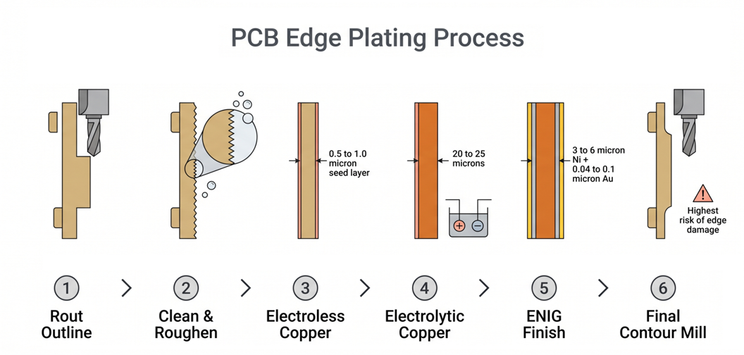
Figure 4: The PCB edge plating process from pre-route to final contour milling
Routing leaves a smear of softened epoxy across the cut face. The bit generates enough friction to melt resin and drag it over the glass bundles. Copper will not adhere to that smear, so the panel goes through a desmear stage. Fabricators use either a permanganate chemical etch or a plasma cycle. Missing that step is the usual cause of edge plating that lifts off months later. Bit diameter matters more than it first appears. A small bit deflects under load and leaves a wavy wall that plates unevenly. Most fabricators stay at 1.6 mm (63 mil) or larger for a plated profile. Every inside corner, therefore, carries a radius of half the bit diameter, so a plated pocket cannot have a sharp 90-degree internal corner.
Electroless Copper Deposition and Electroplating
Copper will not electroplate onto glass and epoxy. An electroplating bath needs the surface to conduct current already. The routed wall is an insulator, so the panel first passes through an electroless copper line. A palladium catalyst is adsorbed onto the bare laminate. A chemical reduction then deposits copper onto it with no external current at all. The electroless film is only 0.5 to 1 micron thick, far too thin to carry useful current. Its only job is to make the wall conductive. The acid copper sulfate bath that follows can then plate onto it properly.
Plating thickness, process time, and acceptance criteria depend on the fabricator, applicable standard revision, product class, and customer specification. Confirm the required plated-edge construction and inspection method with the fabricator; do not transfer through-hole or edge values to a different product without that confirmation.
Surface Finishing and Final Contour Milling
Solder mask has to be kept clear of the plated band. Mask is a cured polymer, so no surface finish will deposit through it. Most fabricators open the mask 0.5 to 0.6 mm (20 to 24 mil) back from the outline. Leaving it closed gives an edge plated in copper but never finished. That edge oxidizes within weeks and then refuses to take solder.
- ENIG is the only finish most fabricators use on plated edges, and JLCPCB states plainly that HASL is not supported there. Hot-air solder leveling blows molten solder off the board using air knives. Those knives cannot control the thickness on a vertical wall, so the solder beads are uneven along the profile.
- Electroless nickel immersion gold plates conformally instead. It lays 3 to 6 microns of nickel under 0.05 to 0.1 microns of gold. The wall, therefore, keeps a flat, solderable and corrosion-resistant skin all the way round.
The board is still attached to its production panel by three or four tabs. Milling those tabs through is the final operation. Wherever a tab is cut, the plating is cut with it. Every plated board, therefore, ends up with unplated gaps somewhere in its edge. JLCPCB asks for at least three breaks of around 3 mm (118 mil), and more on larger boards. Unplated gaps are not a defect, but they are a design input you should control. Leave the choice to the fabricator, and a break can land in the middle of a shield wall.
Essential Design Guidelines for Successful Edge Plating
Clearance and Keep-out Zone Requirements
Every clearance rule for a plated edge comes from one fact. The copper does not stop at the outline; it wraps around it. Plating reaching 0.5 mm (20 mil) onto the outer surfaces will short to anything inside that band. So the keep-out is not measured from the board edge at all. It is measured from the inner boundary of the wrap.
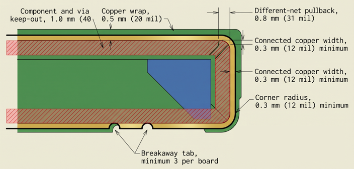
Figure 5: Annotated keep-out zones and clearances around a plated board edge
Inner layer planes are the most dangerous case. A power plane that runs out to the profile touches the plated wall. That shorts the rail straight to chassis ground, usually the first time the board is powered. Pull every non-ground plane back at least 0.25 mm (10 mil) from the outline. Use 0.5 mm (20 mil) wherever the layout allows it. Ground planes are the deliberate exception, since connecting them is the whole point of the feature.
| Feature | Absolute Minimum | Recommended Production Value | Why It Matters |
|---|---|---|---|
| Ground pour past outline | 0.3 mm (12 mil) | 0.5 mm (20 mil) | Gives the plating foil to wrap onto and bond to |
| Non-ground plane pullback | 0.25 mm (10 mil) | 0.5 mm (20 mil) | Stops a power rail from shorting to chassis ground |
| Signal trace to plated edge | 0.3 mm (12 mil) | 0.5 mm (20 mil) | Wrap reaches traces that clear a normal edge |
| Component body to plated edge | 0.5 mm (20 mil) | 1.0 mm (40 mil) | Room for the wrap, the fillet, and a soldering iron |
| Solder mask opening band | 0.5 mm (20 mil) | 0.6 mm (24 mil) | Surface finish cannot be deposited through a cured mask |
| Unplated break length | 3 mm (118 mil) | 5 mm (197 mil) | Tab site with enough material to hold the board |
The middle column is what an experienced designer actually draws. Each of those values buys margin against the failure named beside it, and none costs board area you were using. Build the same numbers into your PCB design rules as a plated-edge rule set. The DRC then catches a violation while you can still move the part.
Choosing the Right Panelization and Breakaway Tabs
V-scoring and edge plating cannot be combined, which catches most designers out the first time. A V-cut blade shears a groove into the board from both faces. It cuts the plated wall lengthwise and tears copper along the whole score line. Panels with plated edges must be tab-routed instead, so the usual V-cut panelization standards do not apply here.
Laying out a plated panel is a short sequence. Work through it in this order, because each step depends on the one before it:
- Mark the edges you want plated on a dedicated mechanical layer, then name that layer in your fabrication notes.
- Place three to four breaks of at least 3 mm (118 mil) on edges carrying no shield wall, connector, or RF block.
- Keep tab spacing under about 75 mm (3 in) so the board cannot sag or chatter against the router.
- Extend the ground pour 0.5 mm (20 mil) past the outline everywhere except inside the breaks.
- Confirm that no non-ground copper crosses the wrap band on any layer, including inner layers.
Depaneling leaves a small burr of copper and laminate at every break. The router is cutting through plated material at exactly those points. Snapping a mouse bite by hand gives the roughest finish, so use a pizza wheel router or a file. On shielded designs, put the breaks on the edge furthest from the antenna. A 5 mm (197 mil) gap is a twentieth of a wavelength at 3 GHz, which is where a shield slot begins to leak.
Why JLCPCB is Your Trusted Partner for Reliable Edge Plating
Precision Manufacturing and Strict Quality Assurance with JLCPCB Edge Plating
JLCPCB edge plating runs through the same electroless and electrolytic line as its through-hole plating. Adding the feature, therefore, does not extend the lead time on a standard build. The published limits are narrow, so they are worth checking before you route the outline. A board that falls outside them gets quoted manually or sent back with a question.
Figure 6: Plated-edge boards under inspection on a production line
- Surface finish: ENIG only, since air knives cannot level molten solder on a vertical wall.
- Minimum board size: 10 x 10 mm (394 x 394 mil), because a smaller panel cannot be held securely while it is routed.
- Minimum board thickness: 0.6 mm (24 mil), below which the wall is too shallow to plate evenly. Our guide to choosing PCB thickness covers the trade-offs.
- Unplated breaks: at least three, and more on larger boards, to leave room for panel support tabs.
- Routing tolerance: plus or minus 0.2 mm (8 mil) standard, or 0.1 mm (4 mil) with high precision milling.
- Castellated holes: 0.5 mm (20 mil) minimum diameter, 1 mm (39 mil) hole to board edge, 0.5 mm (20 mil) hole to hole.
Ordering is where most first attempts go wrong. Edge plating cannot be inferred from a normal Gerber set, because nothing in those files describes it. Select the edge plating option when you order, then upload an annotated diagram or a separate layer.
Cost-Effective Custom Prototyping and Scalable Volume Production
Prototype pricing is what makes plated edges practical to try. The feature has traditionally been treated as a specialty process with a specialty price. Standard two-layer boards start at $2 for five pieces, with one to two days of production. Edge plating is added as an option on that same order, not as a separate quotation. Testing whether a plated edge fixes your emissions problem costs less than the chamber time.
The same panel layout, break positions, and ENIG finish carry straight through. What improves is panel utilization, so the cost per board falls as more copies fit a panel. Send the identical Gerbers and the identical plating layer for the volume order. The shield geometry stays unchanged, which matters once a product has passed emissions testing.
Radio modules are easy to source from the JLCPCB parts library. Check availability there while you are still laying out the carrier board. Once the outline, the breaks, and the wrap are drawn, upload the files to the JLCPCB quote page. Select edge plating, and the price updates before you commit to anything.
FAQ about pcb edge plating
Q: What is PCB edge plating in simple terms?
It is copper-plated onto the vertical side wall of a board, joining the top copper layer to the bottom copper layer around the outside. The perimeter becomes a conductor instead of bare laminate, so it can shield, ground, and be soldered.
Q: Does edge plating actually reduce EMI, or is it marketing?
It genuinely reduces radiated emissions, because the gap between two ground planes at the board edge behaves like the open mouth of a waveguide. Plating that gap closes it, so field energy becomes surface current and returns to ground instead of radiating.
Q: Can the entire board edge be plated with no gaps?
No, because the board stays attached to the production panel by tabs while it is plated. Milling those tabs at the end removes plating locally. Most fabricators require at least three unplated breaks, so nominate their positions yourself.
Q: What is the difference between edge plating and castellated holes?
Edge plating is a continuous copper wall along the profile, while castellated holes are plated half-holes with bare laminate between them. Castellations are used for solder connections on modules, whereas a continuous plated edge is used when you need a shield.
Q: Why can I not have HASL on a plated edge?
HASL uses air knives to blow molten solder off the board and level it, and that process cannot control the thickness on a vertical wall. The result is beaded, uneven solder along the profile, so fabricators use ENIG on plated edges instead.
Conclusion
PCB edge plating earns its place when a board is part of a shield, a ground path, or a mechanical assembly. It stops being worth the trouble when none of those apply. The physics is simple once you see the board edge as a doorway between two ground planes. Most of the design work is just pushing copper out to the profile instead of pulling it back.
Get the wrap, the plane pullback, and the break positions right, and the rest happens in the tanks that already plate your vias. Shielding requirements keep tightening as Wi-Fi 6E, 5G, and automotive radar push designs past 6 GHz. Every unplated millimeter of board edge matters more at those frequencies. A plated prototype costs little more than a standard board, so test it on hardware rather than argue about it in review.

Popular Articles
• Understanding the Basics of Electronic Devices and Circuits
• Understanding Digital Circuit Timing: Setup Time, Hold Time, Contamination Delay & Clock Skew
• PCBs Explained: A Simple Guide to Printed Circuit Boards
• Guide to the Top 10 Commonly Used Electronic Components
• Digital 101: Fundamental Building Blocks of Digital Logic Design
Keep Learning
A Beginner's Guide to Printed Circuit Board Repair: Common Issues, Methods, and Solutions
Key Takeaways Understand PCB structures, components, and common failure causes to identify repair challenges effectively. Follow a systematic PCB repair process, from fault diagnosis and component replacement to testing and verification. Know when PCB repair is practical and when remanufacturing a new PCB provides a more reliable solution. A printed circuit board (PCB) is a critical part of almost every electronic device. When a board fails, the problem may come from damaged components, broken copper ......
The Hardware Development Process: From Concept to a Finished Electronic Product
Key Takeaways A structured hardware development process turns concepts into functional products through key development stages. Proper PCB design balances performance, manufacturability, and reliability. Early manufacturing considerations help reduce risks and improve prototype success. A reliable PCB partner enables smoother transitions from design to production. Every electronic device you have ever used began as a single idea. A desk lamp that brightens with a tap, a wireless earbud, a controller i......
Demystifying Bare PCB Quality for Reliability-Critical Applications
Key Takeaways Early Defect Catching: Catching faults at the bare board stage costs only the PCB, avoiding wasted components and rework later. Perfboard Risks: Zero PCBs lack reference planes and plated holes, causing signal noise above 10–20 MHz and pad lifting. Critical Material Specs: Reliability depends on hole barrel copper (20–25 µm), Tg, Td, and CTI ratings matching your operating environment. Finish & Shelf Life: HASL and ENIG last ~12 months, while OSP and Immersion Silver/Tin expire in ~6 mon......
A Comprehensive Guide to Capacitor ESR: What It Is, Good Values, and How to Measure It
Key Takeaways Definition: Capacitor ESR (equivalent series resistance) is the single resistance that represents the losses inside a real capacitor, from its electrodes, terminations, electrolyte, and dielectric. Why It Matters: Ripple current flowing through the ESR produces a ripple-voltage step on the supply rail and I²R heating in the capacitor, which limits the capacitor's ripple-current rating and service life. Conditions Matter: ESR varies with frequency, temperature, capacitance, case size, and......
Understanding IPC-6012 Standards for High-Reliability Rigid PCB Fabrication
Key Takeaways IPC-6012 vs. IPC-A-600: IPC-6012 is the binding specification, while IPC-A-600 is only for visual reference. Class 2 vs. Class 3: Class 3 requires thicker copper (25μm vs. 20μm) and zero plating voids. Coupon Verification: Quality is tested by microsectioning panel coupons after thermal stress. Upfront Callout: Specify the class on drawings upfront; boards cannot be upgraded later. IPC-6012 is the line on your fabrication drawing that decides what your supplier is allowed to ship. Most d......
Mastering PCB Plating Types and Process Control in High-Yield Fabrication
Key Takeaways Two-Step Plating: Chemical seed layer comes first, electrolytic copper adds structural strength. Process Choice: Pattern plating enables fine tracks; panel plating suits heavy copper. Via Integrity: Keep aspect ratio ≤ 10:1 to prevent thinnest-point barrel cracking. Surface Finishes: Use ENIG for flat BGA pads and hard gold for high-wear contacts. IPC Standards: Class 2 mandates 20μm copper wall thickness; Class 3 requires 25μm with zero voids. PCB plating turns a stack of drilled lamina......