Can PCB Autorouters Really Deliver Production-Ready Designs?
19 min
- What Is PCB Autorouter and How Does It Work?
- Where PCB Autorouting Fits Into the Design Process
- What PCB Autorouters Do Well and Where They Fall Short
- Choosing the Right PCB Autorouter Software
- Turning an Autorouted PCB Into a Manufacturable Design
- How Professional PCB Manufacturers Validate Autorouted Designs
- FAQ About PCB Autorouter
- Conclusion
Key Takeaways
- Rules over DRC: A clean DRC only proves rules were followed, not that the board works.
- Placement First: Autorouters cannot compensate for bad component placement.
- Selective Automation: Hand-route power, analog, and high-speed traces; autoroute only repetitive or low-speed nets.
- DFM Validation: Verify real manufacturing tolerances before sending files to production.
Every PCB autorouter sells the same promise: press one button and watch the ratlines turn into copper. On a simple two-layer breakout it usually delivers. On a mixed-signal board with a fine-pitch BGA and a switching regulator, the result is something you would never have drawn by hand.
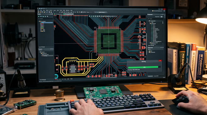
Figure 1: A dense autorouted PCB layout
Your design rules are that map, and anything you never encoded stays invisible to the algorithm. That is why an autorouted board can pass every design rule check and still ring, radiate, or sag under load. This guide covers what automated routing genuinely does well, and where it fails and why. It also shows how to fairly compare autorouter software. Then it covers what has to happen before an autorouted board is safe to manufacture.
What Is PCB Autorouter and How Does It Work?
Automated routing is a constraint solver dressed as a layout tool. It turns your rules into copper, so most of the quality is decided before you press the button.
What Is PCB Autorouter?
A PCB autorouter is a software engine that turns unrouted connections into physical copper. It reads the ratlines from your netlist and searches for a legal path for each one. Legal means it obeys the constraints you set: track width, clearance, permitted layers, and via styles. Nothing else guides the search, so the rule set is effectively the design.
Altium's Situs Topological Autorouter shows how that search actually works. It triangulates the space between obstacles and plans a human-like path from relative positions rather than from a fixed grid. That topological path is then converted into real copper by a sequence of routing algorithms. Because there is no grid, the router is never forced onto an arbitrary pitch.
How Automated PCB Routing Works With Design Rules
Design rules are the entire input, and a router will use every millimeter of freedom you give it. Allow 0.10 mm (4 mil) tracks at 0.10 mm (4 mil) spacing, and it will use both, because finishing the net is the only outcome its objective function rewards. Nothing in the algorithm favors a conservative track over a legal minimum.
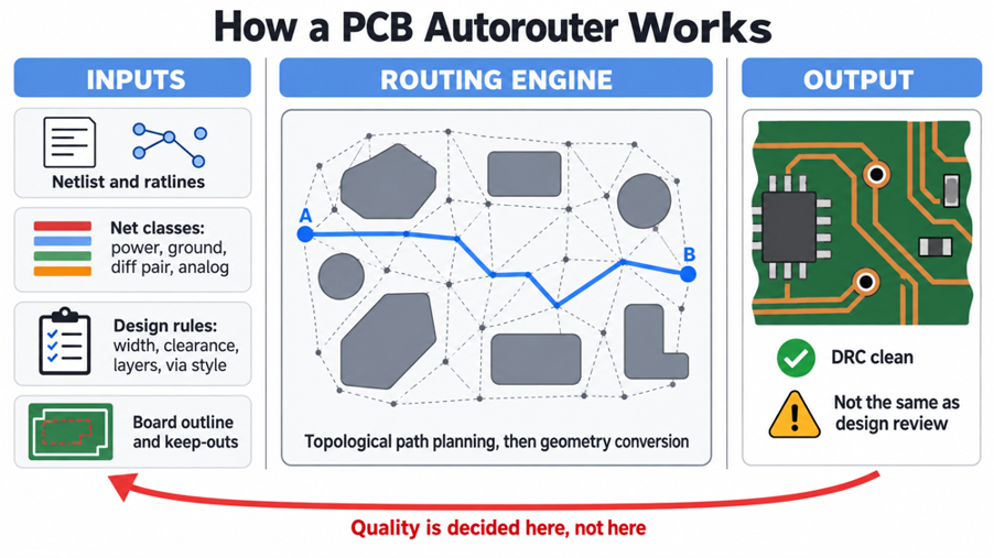
Figure 2: How design rules, net classes, and the routing engine relate
Your fabricator's minimum is a process limit and not a target, which is the distinction most rule sets get wrong. A board built at the absolute edge yields worse than one built with a margin. A good setup separates the nets into classes before anything is routed. Power nets get wider tracks, differential pairs get a matched width and gap rule, and critical analog nets get excluded entirely. Read through PCB design rules and best practices once while you build that class list. A missing class is the most common reason an autorouted board comes back wrong.
Work through this sequence before you run any router:
- Define net classes: power, ground, high-speed differential, analog, and general I/O.
- Set a width and clearance rule for each class, with a margin above your fabricator's minimum.
- Set via styles, and where it matters, a maximum via count per net.
- Restrict layers per class, so a clock net cannot wander onto a layer with no adjacent reference plane.
- Route the nets you care about by hand, then lock them so the router treats them as obstacles.
- Run the router on what is left, and review every net it touched.
- A router does not make routing decisions. It carries out the decisions you already wrote down as rules.
Where PCB Autorouting Fits Into the Design Process
Routing sits fourth in a chain that begins with the schematic, and the steps before it set a ceiling no router can climb past. Placement determines most of the outcome because it determines how far each connection has to travel.
From Component Placement to PCB Routing
Placement quality dominates routing quality, and no autorouter compensates for a bad one. If two connected parts sit at opposite corners of the board, every router produces a long trace, because that is the only path available to it. Move the parts closer, and the same tool produces a short one.
Decoupling capacitors are the second placement decision the router will not fix for you. A 100 nF capacitor has to sit within a few millimeters of the pin it serves, with a short path down to the plane. That is because loop inductance limits how fast charge arrives. An autorouter that connects it via a long trace has satisfied connectivity requirements and destroyed decoupling.
What a PCB Routing Tool Can Automate
Automation earns its place in work that is repetitive, geometrically regular, and fully rule-based. That covers more of a typical board than autorouter skeptics admit. It stops earning that place once physics matters more than connectivity.
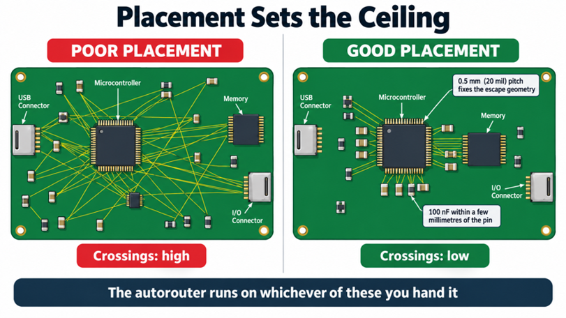
Figure 3: The same board placed well and placed badly, with ratlines shown
- Fanout and escape routing: BGA and fine-pitch QFN pads each need a via and a short stub, so the pattern repeats hundreds of times identically, and the rules describe it completely.
- Bus and parallel group routing: Guided routers such as Altium's ActiveRoute or Siemens' Xpedition Sketch Router follow the path you draw, preserving bus ordering rather than scrambling it.
- Length tuning: Serpentine insertion to a target length is arithmetic, so a tool does it faster and far more accurately than you will by hand.
- Copper pours and thermal relief: Pour generation, spoke thermal relief, and via stitching are all rule-driven, which is why they were automated long before routing was.
- Low-speed I/O and status nets: Nothing about a button, an indicator LED, or a 100 kHz I2C line depends on the path taken, only on the connection existing.
- Teardrops and cleanup: Adding teardrops at the pad and via junctions is a geometric operation applied uniformly across the whole board.
Copper pour is worth treating separately, because routers and pours interact badly. A router finishing late will drop vias into a plane region and split it, so a pour that looked solid becomes a maze of narrow necks.
What PCB Autorouters Do Well and Where They Fall Short
The honest answer to the question in the title lives in this section. Autorouters are genuinely good at a defined class of work and unreliable outside it, so the skill is knowing which nets belong on which side of that line.
Handling Repetitive and High-Density Routing Tasks
Density is where automation pays for itself. A 484-ball BGA on a six-layer board needs hundreds of escape vias, each on the same relative offset. Doing that by hand costs a day of tedious work with no engineering content in it. A router produces the same pattern in seconds, so that day simply disappears.
That multi-layer pass also spread traces more evenly, which left more room for length tuning. Wide parallel buses are the second clear win, provided you use a guided router rather than a fully automatic one.
| Routing Task | Automate It? | Why | What You Should Do |
|---|---|---|---|
| BGA and connector fanout | Yes | The geometry repeats identically, and the rules describe it fully | Let the router do it, then check via style and count |
| Wide parallel buses | Mostly | Topology is regular, but ordering matters to you | Use a guided router and draw the path yourself |
| Low-speed logic and I/O | Yes | Nothing depends on the path, only on the connection | Autoroute, then review clearances |
| Controlled impedance pairs | Partly | Width is a rule; plane continuity underneath is not | Route by hand, or lock the pair and verify the reference |
| Switching regulator loops | No | Loop area sets radiated noise, and no rule expresses it | Hand route the input loop before running anything |
| Analog and sensor front ends | No | Coupling and return path matter more than the connection | Hand route, then keep the router out of those nets |
Signal Integrity, Power Distribution, and Complex Constraints
Signal integrity is where the model breaks down, since the things that matter are not expressible as clearance rules. A router checks that two traces sit far enough apart. It never checks whether the return current under one of them has a continuous path home.
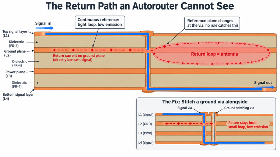
Figure 4: Return current path under an autorouted signal
- Return paths are easy to miss. A high-speed signal normally returns through the reference plane directly beneath it. If the trace changes layers and the new layer uses a different reference plane, the return current must detour. That larger loop can increase EMI.
- Trace width is easy to enforce; plane continuity is not. An autorouter can hold a width rule, but it may still route an impedance-controlled trace across a split in the reference plane. Critical high-speed routes are therefore better handled manually or locked after review.
- Power loops need more than connectivity. In a buck regulator, the switching loop runs through the input capacitor, the high-side FET, the inductor, and the return path. Keeping that loop area small is essential for reducing radiated noise.
- Thermal limits are also easy to overlook. A router may know the minimum electrical width but not the temperature-rise target. A 3 A power trace on 1 oz copper may need around 3 mm (118 mil) in width to keep the temperature near 10 °C, depending on the actual stackup and conditions.
Why Automated Routing Still Needs Engineering Review
Design rule checking and design review answer completely different questions. DRC asks whether the geometry is legal, so it passes whenever the rules are obeyed. The review asks whether the board will work, a question no rule checker has ever been able to pose. The gap between those two questions is where autorouted boards fail. A clean DRC on an autorouted layout tells you the router obeyed you, and nothing more.
If your rules omitted return path continuity, loop area, and analog isolation, the check passed on a board carrying all three problems. Automatic routers produce traces that wander, buses that scramble, and vias placed to solve a congestion problem; better placement would have removed them. Some of it is harmless, but every unnecessary via is a drilled hole and a plated barrel that can fail.
A passing DRC proves the router followed your rules. Only a human review proves those rules were the right ones.
Choosing the Right PCB Autorouter Software
Autorouter software differs less in raw algorithm than in how much control it hands back to you.
Design Rule Support and Routing Flexibility
Rule depth is the first thing to test, because a router can only respect what it can represent. A tool with a single global clearance value routes a 12 V rail exactly like a logic signal, which is wrong in both directions. Check the following before you trust any engine with a real board:
- Per-class width and clearance: Without it, every net gets identical copper, which is wrong for power and wrong for high-speed.
- Differential pair support: The router has to hold both width and gap along the pair, since impedance depends on the pair behaving as one structure.
- Layer direction and restriction: Forbidding a class from a layer keeps clock nets off any layer with no adjacent reference plane.
- Locking and keep-out honoring: Hand-routed nets must survive untouched, so the tool has to treat locked copper as a hard obstacle.
- Via control: A cap on vias per net stops the router from solving congestion with holes you then pay to drill and plate.
ActiveRoute in Altium Designer is a good example, since it routes only the nets you select along a guide you draw yourself.
Connectivity, Layer Management, and Optimization Features
A router that finishes 98 percent of nets by scattering vias has saved you nothing, since the cleanup can take longer than routing by hand would have. Judge output on via count, trace length distribution, and bus ordering instead.
Routing several layers simultaneously, rather than one after another, produces a more even trace distribution because the engine can trade space between layers as it works. Sequential routers fill the top layer first, then fight congestion on every layer after it.
| Tool | Router | Approach | Best Suited To |
|---|---|---|---|
| Altium Designer | Situs Topological Autorouter | Fully automatic, topological space mapping | Fanout and first-pass routing you intend to rework |
| Altium Designer | ActiveRoute | Guided: you draw a route guide, and it routes selected nets | Buses and groups where ordering matters; fanout must exist first |
| Cadence Allegro X | Allegro PCB Router (formerly Specctra) | Constraint-driven automatic and semi-automatic | Large constraint-heavy boards in a managed flow |
| Siemens Xpedition | Sketch Router (AutoActive) | You sketch a path, the router fills DRC-correct copper | High pin-count designs where intent must survive |
| KiCad 9 and 10 | None bundled; Freerouting via DSN/SES | External Java router through a Specctra file round trip | Hobby and low to medium speed boards, cleanup expected |
| EasyEDA Pro | Built-in cloud or local autorouter | Rule-aware automatic routing, DSN/SES export available | Quick prototypes; the docs state results need manual adjustment |
| Cloud AI routers | Quilter, DeepPCB, and similar | Generate several candidate layouts from constraints | Exploring options, with vendor figures treated as claims |
Integration With the Overall PCB Design Workflow
Integration determines whether automation saves time or merely shifts the work elsewhere. A router built into the PCB editor reads design rules directly, while an external router depends on file exchange.
The usual exchange is Spectra DSN/SES. You export a DSN file containing the board and routing rules, then import the routed result as an SES file. KiCad 9 and 10 use this workflow with Freerouting because KiCad does not include a built-in autorouter. EasyEDA Pro supports both approaches. Its autorouter can run in the cloud or through a local routing service, with controls for layers, via density, priorities, and corner style. EasyEDA also supports DSN/SES exchange for tools such as Freerouting.
The practical approach is simple: use autorouting as a first pass for low-speed nets, then manually route or review high-speed, high-current, and other critical connections.
Turning an Autorouted PCB Into a Manufacturable Design
An autorouted board that passes DRC is not yet a manufacturable board, because DRC only tests the rules you happened to write.
DFM Checks for Trace Width, Spacing, and Vias
Manufacturing limits and design rules are rarely the same numbers. JLCPCB publishes a minimum of 0.10 mm (4 mil) track and space on 1 oz outer copper. Copper weight changes those limits in a way most routers never model. Heavier copper etches with more undercut, so 2 oz copper needs 0.16 mm (6.5 mil) track and space instead.
| Parameter | JLCPCB Published Minimum | Why the Router Will Not Protect You | Rule Value Worth Setting |
|---|---|---|---|
| Track width and space, 1 oz | 0.10 / 0.10 mm (4 / 4 mil) | It uses the smallest legal value to finish nets | 0.15 mm (6 mil) as the default class |
| Track width and space, 2 oz | 0.16 / 0.16 mm (6.5 / 6.5 mil) | Copper weight is invisible to most routing engines | A separate rule set for each copper weight |
| Via hole and pad | 0.15 mm (6 mil) hole, 0.25 mm (10 mil) pad | Vias get added freely to solve congestion | 0.3 mm (12 mil) hole in a 0.6 mm (24 mil) pad |
| Plated hole annular ring | 0.20 mm, 0.25 mm recommended on 1 oz | The ring shrinks silently when the pad and hole rules conflict | Check the ring, not only the hole size |
| Solder mask bridge | 0.10 mm (4 mil) on 1 oz, 0.20 mm on 2 oz | Routing close to pads erodes the mask dam | Keep tracks 0.2 mm (8 mil) clear of adjacent pads |
| Via to track clearance | 0.20 mm (8 mil) | It is treated as any other clearance value | Enter it explicitly, since defaults are often lower |
| Silkscreen line and text | 0.15 mm (6 mil) line, 1.0 mm (40 mil) height | Late vias land on top of the legend | Re-run the silkscreen check after routing |
JLCPCB accepts a 0.15 mm (6 mil) hole in a 0.25 mm (10 mil) pad. That leaves only 0.05 mm (2 mil) of ring on each side, and drill registration eats into it quickly. A default via of 0.3 mm (12 mil) hole in a 0.6 mm (24 mil) pad is a much safer working value.
Reviewing Routing for Fabrication and Assembly Requirements
Fabrication is only half of the review, because a board also has to be assembled. An autorouter has no model of a stencil, a placement nozzle, or a reflow oven, so it will route in ways that quietly make assembly harder.
Silkscreen is the most visible casualty of a late routing pass. Vias placed near the end land on top of reference designators and polarity marks, and the fabricator's software then clips the legend away. JLCPCB's minimum legend line width is 0.15 mm (6 mil) at a text height of 1.0 mm (40 mil), so anything already marginal disappears once a via lands on it.
How Professional PCB Manufacturers Validate Autorouted Designs
A fabricator cannot tell whether your board was routed by hand or by algorithm, and it does not need to, because every check runs on the data rather than the method.
Engineering Review and Manufacturing Data Verification
Verification starts with the data rather than the design intent, because the fabricator never sees your schematic. Your Gerber set, drill file,e and pick-and-place data are read into CAM software. There, the layers are aligned and compared against the process rules for the copper weight and stackup you ordered.
JLCPCB then generates a production file from your original Gerber files, adjusted to its capabilities and production rules. That production file is what actually gets manufactured, so it is the version worth looking at. Orders needing changes are held for confirmation, and production continues only once you approve the revised data. You can upload your Gerbers and order the board from the same quote page you use for a hand-routed prototype. Every limit is listed under JLCPCB's published PCB capabilities.
Fabrication, Inspection, and Reliability Validation
Fabrication validates the routing whether you want it to or not. Etching, drilling, and plating each carry a tolerance, so a design sitting at the process limit has spent that tolerance before manufacturing even begins. Thin tracks suffer first because the etch undercut removes copper from the sides as well as the top.
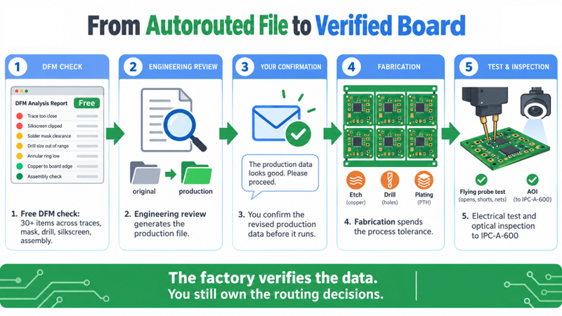
Figure 5: The manufacturing validation path that an autorouted design passes through
- Electrical test catches what geometry checks cannot. Boards are flying-probe or fixture-tested for continuity and isolation against the netlist, so any open track or short between two crowded traces is found before shipping.
- Optical inspection covers the outer layers, and inner layers are inspected before lamination because nothing can reach them afterward. Acceptance is judged against IPC-A-600 for the bare board and IPC-A-610 for the finished assembly.
FAQ About PCB Autorouter
Q: Can I use a PCB autorouter for a high-speed design?
Yes, but only for the fanout and the non-critical nets. Route the differential pairs, clocks, and their return paths by hand first, then lock them so the router treats that copper as an obstacle.
Q: Why did my autorouted board come back with so many vias?
Congestion is the usual cause, and a via is the cheapest way for the algorithm to escape it. Cap the vias per net in your rules and rerun, and if the count stays high, the real problem is placement rather than routing.
Q: Does KiCad have a built-in autorouter?
No. KiCad 9 and 10 ship with interactive routing only, and the legacy autorouter was removed in a previous release. The common workaround is Freerouting, which you feed by exporting a Specctra DSN file from KiCad and then importing it back as an SES session file.
Q: Are AI autorouters better than traditional autorouter software?
They target the right weakness, since they optimize against physical objectives rather than just completing nets. The completion percentages published by those vendors are their own benchmarks with no independent verification, so treat them as illustrations.
Q: Will a PCB manufacturer reject an autorouted design?
Not for being autorouted, because the fabricator only sees Gerber data and cannot tell how it was created. Rejections and revision requests come from the design sitting at or beyond process limits, which autorouted boards do more often.
Conclusion
So can a PCB autorouter deliver production-ready designs? Not on its own and not in one click, though that was always the wrong question to ask. Automated routing reliably handles fanout, buses, length tuning, and low-speed nets when placement is good, and the rule set is complete. It fails on switching loops, return paths, controlled impedance, and analog isolation, because none of those are expressible as clearance rules.
The productive way to use one is as a fast assistant with a narrow brief. Hand route what matters, lock it, class everything else, and let the router finish the tedious remainder under supervision. Then treat manufacturability as a gate separate from correctness, because a legal board is not automatically a buildable one. A free DFM check and a fabricator's engineering review catch process problems that an autorouter can't detect, and both are available before you spend anything.

Popular Articles
• Understanding the Basics of Electronic Devices and Circuits
• Understanding Digital Circuit Timing: Setup Time, Hold Time, Contamination Delay & Clock Skew
• PCBs Explained: A Simple Guide to Printed Circuit Boards
• Guide to the Top 10 Commonly Used Electronic Components
• Digital 101: Fundamental Building Blocks of Digital Logic Design
Keep Learning
A Beginner's Guide to Printed Circuit Board Repair: Common Issues, Methods, and Solutions
Key Takeaways Understand PCB structures, components, and common failure causes to identify repair challenges effectively. Follow a systematic PCB repair process, from fault diagnosis and component replacement to testing and verification. Know when PCB repair is practical and when remanufacturing a new PCB provides a more reliable solution. A printed circuit board (PCB) is a critical part of almost every electronic device. When a board fails, the problem may come from damaged components, broken copper ......
The Hardware Development Process: From Concept to a Finished Electronic Product
Key Takeaways A structured hardware development process turns concepts into functional products through key development stages. Proper PCB design balances performance, manufacturability, and reliability. Early manufacturing considerations help reduce risks and improve prototype success. A reliable PCB partner enables smoother transitions from design to production. Every electronic device you have ever used began as a single idea. A desk lamp that brightens with a tap, a wireless earbud, a controller i......
Demystifying Bare PCB Quality for Reliability-Critical Applications
Key Takeaways Early Defect Catching: Catching faults at the bare board stage costs only the PCB, avoiding wasted components and rework later. Perfboard Risks: Zero PCBs lack reference planes and plated holes, causing signal noise above 10–20 MHz and pad lifting. Critical Material Specs: Reliability depends on hole barrel copper (20–25 µm), Tg, Td, and CTI ratings matching your operating environment. Finish & Shelf Life: HASL and ENIG last ~12 months, while OSP and Immersion Silver/Tin expire in ~6 mon......
A Comprehensive Guide to Capacitor ESR: What It Is, Good Values, and How to Measure It
Key Takeaways Definition: Capacitor ESR (equivalent series resistance) is the single resistance that represents the losses inside a real capacitor, from its electrodes, terminations, electrolyte, and dielectric. Why It Matters: Ripple current flowing through the ESR produces a ripple-voltage step on the supply rail and I²R heating in the capacitor, which limits the capacitor's ripple-current rating and service life. Conditions Matter: ESR varies with frequency, temperature, capacitance, case size, and......
Understanding IPC-6012 Standards for High-Reliability Rigid PCB Fabrication
Key Takeaways IPC-6012 vs. IPC-A-600: IPC-6012 is the binding specification, while IPC-A-600 is only for visual reference. Class 2 vs. Class 3: Class 3 requires thicker copper (25μm vs. 20μm) and zero plating voids. Coupon Verification: Quality is tested by microsectioning panel coupons after thermal stress. Upfront Callout: Specify the class on drawings upfront; boards cannot be upgraded later. IPC-6012 is the line on your fabrication drawing that decides what your supplier is allowed to ship. Most d......
Mastering PCB Plating Types and Process Control in High-Yield Fabrication
Key Takeaways Two-Step Plating: Chemical seed layer comes first, electrolytic copper adds structural strength. Process Choice: Pattern plating enables fine tracks; panel plating suits heavy copper. Via Integrity: Keep aspect ratio ≤ 10:1 to prevent thinnest-point barrel cracking. Surface Finishes: Use ENIG for flat BGA pads and hard gold for high-wear contacts. IPC Standards: Class 2 mandates 20μm copper wall thickness; Class 3 requires 25μm with zero voids. PCB plating turns a stack of drilled lamina......