
Fiducial Marks in PCB and SMT Assembly: A Complete Guide to Accuracy and Design Rules
12 min
- What is a Fiducial Mark?
- Types and Hierarchy of Fiducial Marks: Global, Local, and Panel
- Essential Design Guidelines for Fiducial Marks
- What Happens When Fiducial Marks Are Designed Incorrectly?
- How JLCPCB's SMT Assembly Service Leverages DFM for Accuracy
- FAQ about Fiducial Marks
- Conclusion: Fiducial Marks and SMT Assembly Precision
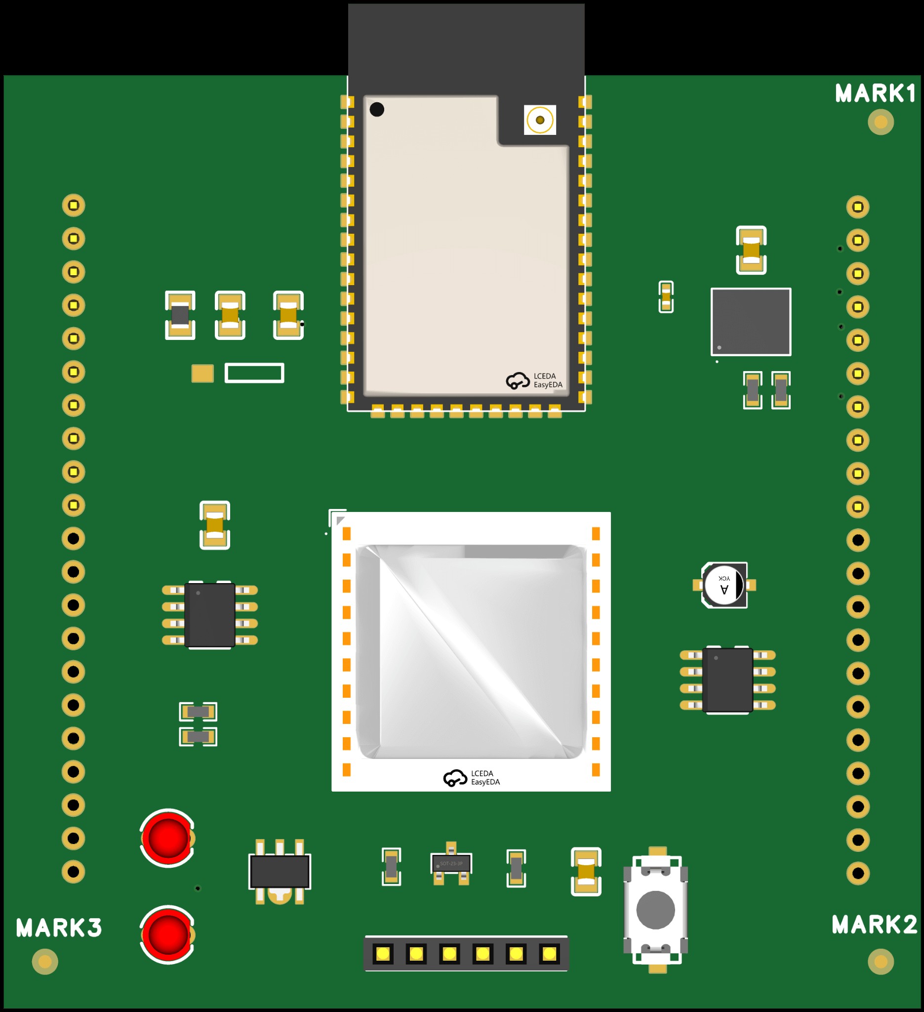
Modern Printed Circuit Boards (PCBs) are complex, integrating high-density components like 0.4mm pitch Ball Grid Arrays (BGAs), 0201 passives, and fine-pitch Quad Flat No-Lead (QFN) packages. In this advanced manufacturing environment, achieving placement accuracy measured in micrometers is crucial.
A significant challenge in automated manufacturing is how pick-and-place machines, which handle thousands of components per hour, precisely locate the PCB. A board on a conveyor system is never in the perfect theoretical position; it will always have minor physical offsets, including a slight horizontal shift, a vertical shift, and a rotational skew. For fine-pitch components, an error of just 0.1mm can lead to assembly defects.
Fiducial marks offer a keen solution for SMT assembly. These precise copper circles function as "GPS coordinates" for the vision system, providing essential registration points for perfect board alignment before solder paste application or component placement.
This article is a technical guide to fiducial marks, covering their function, types, and critical standard design rules for flawless SMT assembly. This precision requires robust design and advanced manufacturing. High-quality PCB assembly service, like JLCPCB, use Design for Manufacturability (DFM) principles to create perfectly assembled products from digital designs.
What is a Fiducial Mark?
A fiducial mark is a specific, high-contrast, non-drilled reference point on the PCB surface. It is designed solely to be recognized by the machine vision systems on automated SMT equipment, including stencil printers, pick-and-place (PnP) machines, and Automated Optical Inspection (AOI) systems.
How Fiducial Marks Enable Vision Alignment and Correction
Fiducial marks act as a bridge between the ideal digital world of your CAD file and the imperfect physical reality of the production line. Here is a step-by-step breakdown of the correction process:
-
Board Loading
The PCB is loaded into the machine (e.g., a stencil printer).
-
Expected Location
The machine's camera moves to the anticipated location of the first fiducial, as defined by your Gerber and centroid (pick-and-place) files.
-
Actual Location
The camera captures an image, identifies the precise center of the fiducial, and records its (X, Y) coordinates.
-
Repetition
This process is repeated for the second and third fiducials.
-
Offset Calculation
The machine's computer compares the expected and actual coordinates to calculate the exact X-axis offset, Y-axis offset, and rotational offset. Finally, the machine applies this correction matrix to the entire placement program for that specific board. This ensures that every component is placed relative to the board's actual position, not its theoretical one, compensating for any skew or shift.
Types and Hierarchy of Fiducial Marks: Global, Local, and Panel
To demonstrate true DFM expertise, you must understand that not all fiducials serve the same purpose. Alignment occurs in a hierarchy to account for different types of errors.
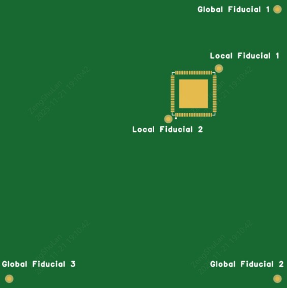
1Global Fiducial Marks
Purpose: To align the entire PCB with the machine's coordinate system, correcting for overall position and rotation on the conveyor.
Placement: A minimum of two, but three fiducial marks are strongly recommended. They should be placed in an "L" configuration (e.g., one near (0, 0), one at (X, 0), one at (0, Y)) and as far apart as possible to maximize accuracy.
Why Three? While two fiducial marks can correct X, Y, and rotational offsets, three marks offer unambiguous alignment. This also enables the detection of board scaling or stretching errors during fabrication.
Requirement: For a double-sided SMT assembly, you must have a set of global fiducials on both the top and bottom sides of the board.
2Local Fiducial Marks
Purpose: To correct the alignment of high-precision components, such as BGAs, QFPs, and QFNs, specifically those with a pitch of 0.5mm or less.
Why Global Isn't Enough: FR-4 laminate is not a perfectly stable material. It can slightly warp, stretch, or shrink during the fabrication and reflow soldering processes. Over a large board, this minor distortion (e.g., 100 ppm) can cause a 0.01mm error at a component far from the global fiducials. This is more than enough to cause shorts on a fine-pitch part.
Function: The machine first locates the board using global fiducials. Then, it moves its camera to the specific component and uses local fiducials for a second, highly accurate correction immediately before placement.
Placement: Typically, two fiducial marks are placed diagonally opposite the component's land pattern.
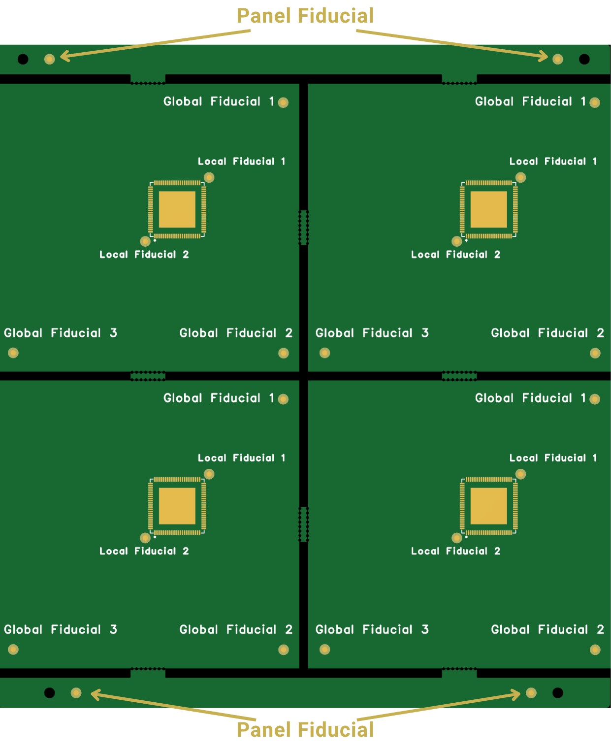
3Panel (Array) Fiducial Marks
Purpose: These fiducial marks are used in the manufacturing process when multiple printed circuit boards (PCBs) are produced together as a single array, also known as a "panel."
Placement: Unlike global fiducials found on individual boards, panel fiducials are not located on the PCBs themselves. Instead, they are placed on the "tooling rails" or "waste strips" that surround the array.
Function: Their primary function is to align the entire panel for critical manufacturing steps, such as stencil printing and pick-and-place operations. This initial panel alignment may or may not be followed by the use of global fiducials for more precise alignment of individual boards within the panel.
Essential Design Guidelines for Fiducial Marks
A fiducial mark is effective only when the vision system can detect it clearly and without ambiguity. Adhering to industry-standard fiducial designs is essential for reliable PCB assembly.
Shape and Size
Shape: The universal standard for vision systems is a solid-filled circle. Its center is easily calculated by vision algorithms, regardless of its orientation. It is best to avoid intricate shapes such as squares, diamonds, or crosshairs, as they are less dependable and can impede the vision system's efficiency.
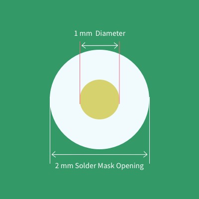
Size: A common and reliable standard is a copper pad with a diameter of approximately 1.0 mm (40 mil).
Solder Mask Clearance
Rule: The fiducial must be exposed copper and free of any solder mask.
Requirement: The solder mask opening should be at least twice the diameter of the fiducial pad. For a 1.0 mm pad, a 2.0 mm (or larger) mask opening is ideal.
Why? This creates a high-contrast ring of bare substrate (e.g., green FR-4) around the shiny copper mark, making it easy for the camera to distinguish.
Copper Clearance
Rule: Maintain a "keep-out" area around the fiducial pad. This area should be equal in size to the solder mask clearance (e.g., 2.0 mm in diameter).
Why? To prevent the vision system from miscalculating the center, a clear zone free of other copper features (traces, planes, vias, text) is necessary. This avoids confusion from nearby reflective features.
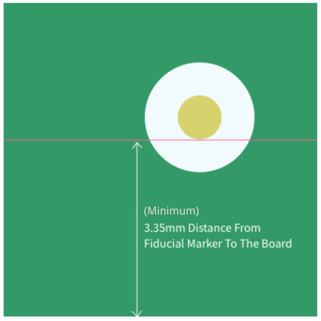
Minimum Distance from Board Edge
Rule: A clearance of at least 3.35 mm is necessary between the board edge and the fiducial mark, including its clearance area.
Why? This specific clearance is crucial to ensure the fiducials are not obscured by the clamps, rails, or tooling fixtures that hold the PCB in place on the conveyor.
Surface Finish
The surface finish of your PCB plays a role in how easily a vision system can read the fiducial marks. JLCPCB offers a range of finishes, and choosing the right one can optimize your design for PCB assembly.
-
Flat and Low-Reflective Surface
A flat, less-reflective finish like ENIG (Electroless Nickel Immersion Gold) or OSP is ideal. It provides a very flat, consistent surface with excellent contrast, which allows the vision system to calculate the fiducial's center with maximum accuracy. This is the recommended choice for designs with ultra-fine-pitch components (e.g., 0.4mm pitch BGAs).
-
Cost-Effective but Less Precise
HASL (Hot Air Solder Leveling), which JLCPCB offers in both leaded and lead-free options, is a very common and reliable choice. However, the HASL process leaves a slightly uneven, domed, and reflective solder surface on the pad. While this is perfectly acceptable for most standard SMT designs, the uneven surface can be more challenging for a vision system to read with high precision than a perfectly flat ENIG finish.
What Happens When Fiducial Marks Are Designed Incorrectly?
Failing to include correct fiducials is one of the most common DFM errors. The consequences are immediate and costly:
- Assembly Rejection: Your manufacturer will put your job on hold. Their automated SMT line simply cannot run without valid reference points.
- Solder Paste Misalignment: The stencil printer is the first machine to use fiducials. Misalignment at this stage leads to solder paste being deposited off-pad, which inevitably causes defects.
-
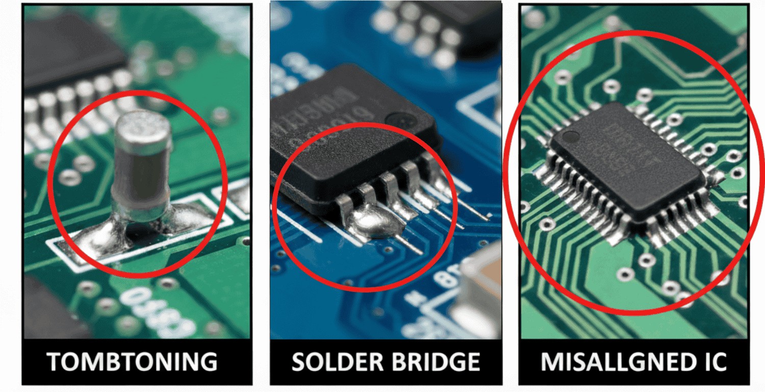
Soldering Defects: Misaligned solder paste leads directly to:
- Solder Bridges: Solder paste bridges two fine-pitch pads, causing shorts.
- Open Circuits: Solder paste doesn't fully cover the pad, leading to no connection.
- Tombstoning: One pad of a passive component gets the correct amount of paste, but the other doesn't, causing the part to pull upright like a "tombstone" during reflow.
- Component Misplacement: This leads directly to shifted or rotated components. For BGAs or QFNs with hidden pads, this is a catastrophic failure, often undetectable without X-ray inspection.
Design for Manufacturability
These issues highlight the critical importance of DFM. Partnering with an advanced PCB assembly manufacturer becomes a major advantage. JLCPCB's SMT assembly service incorporates automated DFM checks that can help flag potential fiducial errors before production begins, saving you from costly rework and delays. JLCPCB also offers a free online DFM tool.
How JLCPCB's SMT Assembly Service Leverages DFM for Accuracy
A well-designed fiducial is crucial for "Design for Manufacturability," effectively communicating project requirements to the SMT assembly line. At JLCPCB, our SMT assembly process leverages your design's DFM features:
- Advanced Vision Systems: Our SMT lines are equipped with high-speed vision systems that automatically detect and correct for board offsets using your fiducial marks. This automated precision enables accurate placement of components as small as 01005.
- Automated DFM Analysis: When you upload your Gerber and centroid files, our online quoting system provides an instant DFM review, catching common mistakes before they become production issues.
- Integrated Quality Control: This precision throughout the entire operation — from solder paste printing to pick-and-place and final AOI — ensures the highest possible yield and reliability for your project.
FAQ about Fiducial Marks
Q: Do I need fiducial marks for a single-sided board?
Yes. Even for a single-sided assembly, you still need global fiducials on that side. Both the stencil printer (for applying solder paste) and the pick-and-place machine need to align the board before they can do their jobs.
Q: Can I use a via or a tooling hole as a fiducial?
No. A tooling hole is a physical mounting hole; it is not an optically precise feature and is far too large. A via is also unsuitable, as it is often "tented" (covered in solder mask) or filled, and its annular ring is not a reliable target. You must always use a dedicated, circular copper pad with a proper solder mask clearance.
Q: My CAD software (KiCad/Altium/Eagle/EasyEDA) has a "fiducial" component. Is that enough?
Yes, it is recommended to utilize your CAD software's integrated fiducial part from its library. These components are typically pre-configured to comply with IPC standards (for example, a 1mm pad with a 2mm mask opening) and ensure that the pad is not tented by the solder mask.
Q: Can fiducials be covered by silkscreen?
No, you should never place a silkscreen over a fiducial mark. The fiducial must be bare copper (with its surface finish) and have a clear solder mask opening. Any ink from the silkscreen layer will obstruct the camera's view, break the visual contrast, and make the fiducial unusable.
Q: What should I do if my board is very small and has no space for global fiducials?
This is a common issue for tiny boards (e.g., in wearable tech). This can be resolved through panelization, where multiple small boards are arranged on a larger panel. The larger panel will use "panel fiducials" on its tooling rails for alignment by the assembly machine. Although panelization handles the main alignment, it is still recommended to include local fiducials for any fine-pitch components on individual boards, if practical.
Q: Where should I place fiducials on a round or oddly-shaped PCB?
For accurate machine placement, three global fiducials should be positioned on the board's outer edge. These should be spaced approximately 90 degrees apart (e.g., 0, 90, and 180 degrees) in a non-symmetrical, non-linear "L" pattern. This configuration allows the machine to precisely determine the board's center and rotation without ambiguity.
Conclusion: Fiducial Marks and SMT Assembly Precision
Fiducial marks are essential, not optional, for any PCB undergoing automated SMT assembly. They are the crucial connection between your CAD file's digital accuracy and the physical manufacturing process. Taking a few minutes to correctly incorporate three global fiducials and any necessary local fiducials into your design will prevent significant delays, expensive rework, and disastrous PCB assembly failures. An understanding of these DFM principles extends beyond mere PCB design; it is integral to ensuring a successful, high-yield production run.
Once the PCB design phase is complete, that precision can be validated with JLCPCB's reliable and cost-effective SMT assembly service.
Popular Articles
• How to Create a Bluetooth-Controlled Car With Arduino: A Step-by-Step Guide
• How to Design and Assemble a Reliable ESP32 Module PCB on a 2-Layer Board
• The Ultimate Guide to Relay Symbol: Coil, Contacts, Diagrams, and Circuit Applications
• How to Identify SMD LED Polarity: Markings, Testing, and PCB Tips
• The Ultimate Guide to PCBA: Process,Types and Techniques for the Electronics Enthusiast
Keep Learning
How to Design an ESP32-S3 Development Board from Scratch: A 4-Layer PCB Design Tutorial
Designing your own ESP32-S3 development board gives you complete control over your hardware architecture while preparing your IoT projects for commercial production. Instead of relying on bulkier, off-the-shelf boards, building a custom design allows you to optimize the board space, expose only the required GPIO pins, and integrate peripherals directly onto a single substrate. In this tutorial, we will design a 4-layer ESP32-S3 development board from scratch. We will walk through the entire hardware d......
Arduino LED Driver Tutorial: Control More LEDs with 74HC595 and MAX7219
Arduino GPIO pins run out quickly in larger LED projects. By utilizing dedicated LED drivers and expansion ICs, you can drastically reduce pin usage, eliminate processor-heavy multiplexing loops, and simplify display wiring. In this guide, you will learn the operational architecture, wiring configurations, cascading techniques, and optimization strategies for the 74HC595 shift register and the MAX7219 LED driver. Why Arduino Projects Need LED Driver ICs Arduino GPIO and Current Limitations An ATmega32......
How to Create a Bluetooth-Controlled Car With Arduino: A Step-by-Step Guide
This tutorial walks through the complete engineering and implementation of a two-wheel Bluetooth RC car with an Arduino Nano module on a specially designed PCBA (Printed Circuit Board Assembly). While many hobbyists start by wiring motors and Bluetooth modules with jumper cables on a breadboard, this approach is prone to disconnection and signal noise. This guide upgrades that process by teaching you how to design a professional mainboard. Key Design Features Controller: Arduino Nano used as a plug-in......
Fiducial Marks in PCB and SMT Assembly: A Complete Guide to Accuracy and Design Rules
Modern Printed Circuit Boards (PCBs) are complex, integrating high-density components like 0.4mm pitch Ball Grid Arrays (BGAs), 0201 passives, and fine-pitch Quad Flat No-Lead (QFN) packages. In this advanced manufacturing environment, achieving placement accuracy measured in micrometers is crucial. A significant challenge in automated manufacturing is how pick-and-place machines, which handle thousands of components per hour, precisely locate the PCB. A board on a conveyor system is never in the perf......
Alternating Current vs Direct Current (AC vs DC): What's the Difference?
Electric current flows in two primary forms: alternating current (AC) and direct current (DC). AC periodically reverses direction, while DC flows steadily in one direction. AC powers the industrial and residential electrical grids, while DC powers batteries, electric vehicles, and nearly all modern consumer electronics. Understanding the core differences between AC and DC matters when designing power supplies, selecting electronic components, or laying out printed circuit boards (PCBs). This guide com......
Arduino LED Multiplexing Tutorial: Control More LEDs with Fewer Pins
The Arduino Uno is a powerful tool for prototyping, but driving multiple LEDs directly quickly exhausts its 20 GPIO pins and its 200 mA absolute maximum package current limit. To bypass these hardware bottlenecks, engineers and hobbyists use LED multiplexing to scale display outputs efficiently without upgrading the microcontroller. In this guide, you will learn the core principles of LED matrix scanning, Charlieplexing, refresh timing, ghosting fixes, and practical Arduino code without relying on any......