Guide to Ground Bounce in PCB - Causes, Effects & Prevention
10 min
- Introduction
- Causes of Ground Bounce
- Effects of Ground Bounce on Circuits
- How to Measure Ground Bounce
- How to Reduce Ground Bounce
- FAQs about Ground Bounce
Key Takeaways
Ground bounce is a voltage spike between an IC's die ground and the PCB ground. It happens when current changes fast through parasitic inductance (V = L x di/dt).
Many outputs switching at once, called SSO, make it much worse.
It can cause logic errors, false resets, and ringing on signals.
You measure it with a quiet-low sense line on a scope.
Good decoupling, short ground loops, and slower slew rates fix most of it.
Introduction
A board passes every test on the bench. Then, in the field, it starts dropping bits or resetting for no clear reason.
The parts are right. The schematic is right. Most of the time, this kind of hidden fault is ground bounce, a switching noise problem that only shows up once enough outputs toggle at once.
Ground bounce is not just an IC problem. It is a layout problem too. Good grounding and decoupling can absorb it. A long return path or weak decoupling can make it worse, even with the same chip.
In simple terms, ground bounce is a voltage gap between an IC's internal ground and the PCB ground. It happens when current changes fast through small amounts of inductance in the package and traces.
This guide covers what causes ground bounce, how it affects a circuit, how to measure it, and how to fix it in layout. For more on power delivery, see our guides on Bypass Capacitor in PCB Layout and PDN Design PCB.
Causes of Ground Bounce
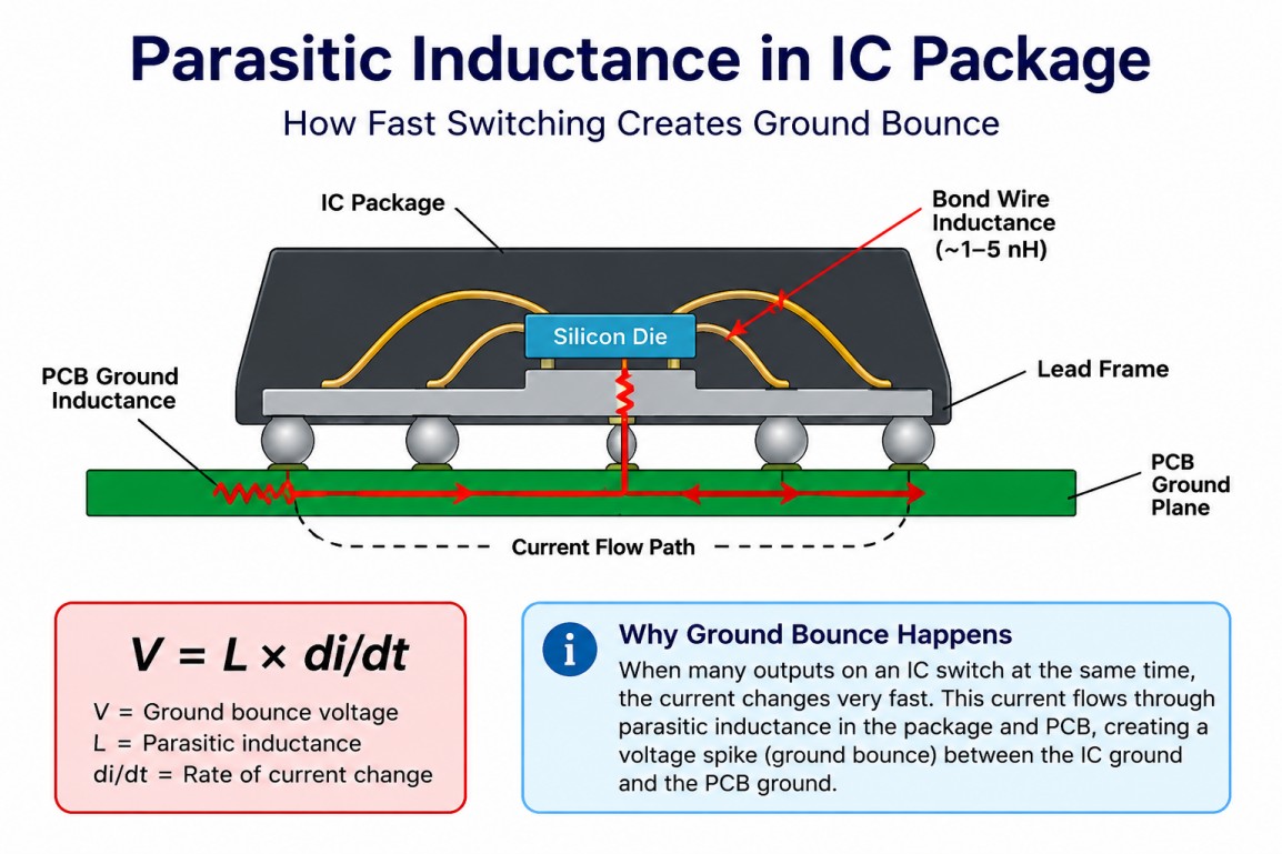
Ground bounce starts inside the IC package, not on the board.
Parasitic Inductance in IC Packages
Every IC package adds a little inductance between the chip and the PCB. Bond wires, the lead frame, and solder balls are not perfect wires.
Think of it as a small inductor sitting between the die's ground and the PCB ground. When a current change hits that inductor, it creates a voltage:
V = L x di/dt
A quick example, using a typical di/dt of 200 A per us, shows how much even a small L adds up:
| Inductance (L) | di/dt | Voltage Spike (V) |
|---|---|---|
| 1 nH | 200 A/us | ~200 mV |
| 2 nH | 200 A/us | ~400 mV |
| 5 nH | 200 A/us | ~1000 mV (1 V) |
A single bond wire might only add 1 to 5 nH. But fast output drivers can push di/dt into the hundreds of amps per microsecond. Even 2 nH can then create a spike of several hundred millivolt.
This is why ground bounce got worse over time. Package inductance barely changed. Switching speed did.
Simultaneous Switching Outputs (SSO)
A single pin switching alone rarely causes trouble. The real problem is SSO, when many outputs on one IC switch together.
Each output adds its own di/dt through the same shared ground path. These add up instead of cancelling out.
This is why wide buses, like DDR memory or parallel GPIO, cause the worst ground bounce. More pins switching together means a bigger spike.
Some datasheets list a max number of outputs that should switch together. Spreading a bus across more ground pins, or more ICs, is a simple fix.
Effects of Ground Bounce on Circuits
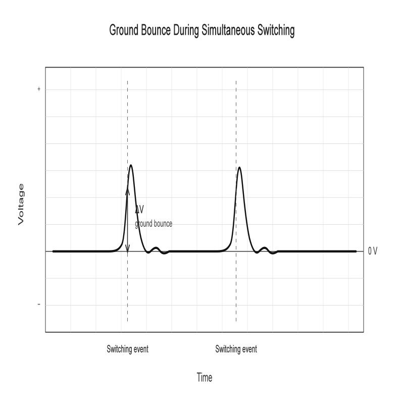
A quiet-low output pin should sit flat near 0V. Ground bounce shows up as voltage spikes riding on top of it during adjacent-pin switching.
When the die ground moves, every signal tied to it moves too. A pin that should sit flat at LOW instead shows a spike.
Example: a 3.3V input with V_IH near 2.0V. A quiet-low pin near 0V can bounce up several hundred millivolts during heavy switching. That may not flip a 0 to a 1, but it eats into the noise margin and can land in the undefined zone between LOW and HIGH.
Use this table to match a symptom to its likely cause:
| Symptom | Likely Cause | Where to Look |
|---|---|---|
| Bit errors under heavy bus use | SSO on a shared ground pin | How many outputs switch together |
| Random reset or lockup | False trigger on reset/CS/interrupt | Timing near nearby switching |
| Ringing after a clean edge | Underdamped RLC return path | Package and trace inductance |
| Fault only at high speed | Faster di/dt than package can handle | Output slew rate |
Logic-Level Shifts and False Triggering
Ground bounce does not just weaken data lines. It can trigger inputs that should not change.
Clocked buses often ignore short glitches. But reset, chip-select, and interrupt lines have no clock to filter noise. A short bounce can trigger a false edge.
A reset line is the worst case. A false trigger can reset a microcontroller with no clear cause. The logs just show a random lockup.
This is why good engineers treat reset and chip-select lines like a clock trace: solid ground underneath, distance from noisy nodes, and sometimes a small RC filter.
Signal Integrity Degradation
Ground bounce also causes ringing that was not in the original signal.
The return path acts like an RLC circuit. A fast edge can excite it into ringing, and most fast digital paths are underdamped, so the ringing does not settle right away.
This ringing shrinks the eye opening on a fast signal and adds jitter. It can even cross the receiver's threshold more than once, causing double-clocking.
Good layout habits, short traces, solid ground planes, small loop area, keep this ringing under control.
How to Measure Ground Bounce
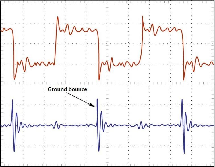
The quiet-low sense line setup: one output pin held LOW while adjacent pins switch, probed directly with a high-bandwidth scope.
You need to see ground bounce before you can fix it. The standard method is the quiet-low sense line test.
Hold one output pin LOW. Switch every other output on the same ground pin. Probe the quiet pin directly. Any voltage you see there is ground bounce, not signal.
A few tips make this measurement accurate:
- Use a scope with at least 1 GHz of bandwidth. Ground bounce spikes are only a few nanoseconds wide.
- Use a short, spring-tip ground connector instead of an alligator clip. A long ground lead adds its own ringing.
- Probe as close to the pin as the package allows.
Check your IC vendor's app notes for exact test conditions. For more on how the ground plane affects this, see our guide on PCB Ground Plane Reduces EMI Noise.
How to Reduce Ground Bounce
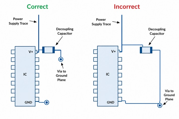
A decoupling capacitor placed within 5 mm of the IC's power and ground pins.
Ground bounce cannot be removed completely. It comes from physics built into every IC package. But it can be pushed low enough to stop causing problems.
| Technique | Effort | Best For |
|---|---|---|
| Decoupling caps near IC pins | Low | Any design, the first fix to try |
| Solid ground plane, short loops | Medium | All fast digital boards |
| Control output slew rate | Low | GPIO, non-critical timing |
| Spread or stagger SSO | Medium | Wide buses, FPGA/CPLD |
| Optimize buck converter loop | Medium to High | Boards with switching regulators |
Use Decoupling Capacitors Close to IC Pins
This is the single best fix, and the cheapest.
Place a 0.1 uF low-ESR ceramic capacitor (0.1 uF is standard, though a combination of 0.1 uF and 10 uF is typically used for dual-capacitance filtering) within 5 mm of the IC's VCC and GND pins. This gives switching current a short loop instead of a long trip through the power and ground planes.
Use several vias to connect the capacitor to the planes, not just one. More vias in parallel means less inductance. If space is tight, place the capacitor on the opposite side of the board, as long as it stays close to the pins.
For more on decoupling and power delivery, see our guide on PCBs Power Integrity Analysis.
Minimize Loop Inductance in PCB Layout
Decoupling caps handle the last few millimeters. Everything past that is loop inductance.
Keep traces short. Route over a solid ground plane, not a split one. See our guide on PCB Ground Plane Reduces EMI Noise for more on this.
On mixed-signal boards, a star grounding layout can keep noisy digital return current away from sensitive analog signals. See our guide on Understanding Star Grounding in PCB Design: A Practical Guide.
Never split a ground plane under a fast signal. Keep return-path vias close to their signal via.
Control Output Slew Rate
Ground bounce comes from di/dt, so a slower edge helps directly.
Many FPGAs and microcontrollers let you adjust drive strength or slew rate per pin. This lowers dv/dt, which lowers di/dt.
The trade-off is timing. A slower edge takes longer to cross the input threshold. Use slow slew for GPIO and non-critical lines. Save full speed for lines that truly need it.
Spread Simultaneous Switching Outputs
If SSO is the main cause, spread the switching out instead of fighting it electrically.
Split a wide bus across more than one IC. This spreads the current across more ground pins. Some FPGA tools also let you add tiny delays between outputs so they do not all switch at once.
Even a small stagger lowers the combined di/dt. This helps most on FPGA designs with wide buses.
Buck Converter Ground Bounce Considerations
Buck converters are one of the worst ground bounce sources on a board.
The real culprit is the input capacitor hot loop: current flowing from the input cap, through the high-side FET, through the low-side FET, and back. This loop can swing several amps per nanosecond.
Keep the ground plane solid under the converter. Keep the input capacitor loop as small as possible. Use a Kelvin ground connection at the controller IC so noisy power current does not share a trace with the sensitive ground pin.
For a full layout walkthrough, see our guide on Effective PCB Layouts for Switching Regulators.
FAQs about Ground Bounce
Q: What is ground bounce?
It is a voltage gap between an IC's internal ground and the PCB ground, caused by fast current changes through small amounts of inductance.
Q: What causes ground bounce in PCB design?
Parasitic inductance in the IC package, plus fast switching current. Many outputs switching together, or SSO, makes it much worse.
Q: How do I know if ground bounce is my problem?
Random resets, false triggers on chip-select or interrupt lines, and bus errors that only show up under heavy switching are common signs. A quiet-low sense line test on a scope confirms it.
Q: How do I fix ground bounce?
Start with decoupling caps close to the IC pins. Then use a solid ground plane. Slower slew rates and spreading SSO help too.
Q: Does ground bounce affect analog boards too?
Yes. Digital ground bounce can couple into a nearby analog ground if they share a return path. Star grounding helps keep them apart.
Conclusion about Ground Bounce
Ground bounce comes from parasitic inductance reacting to fast switching current. It can cause voltage spikes, logic errors, and ringing that are hard to trace.
The fix is mostly good layout habits: decouple close to the pins, keep ground loops short and solid, control slew rate, and spread out SSO on wide buses. Measure with a quiet-low sense line to confirm any fix worked.
Apply these habits on your next board. If you want a second set of eyes on your grounding and decoupling before fabrication, JLCPCB's PCB layout service can check your stackup and layout while it is still easy to fix.
Keep Learning
Bypass Capacitor Placement in PCB Layout: Best Practices
Quick answer:Bypass Capacitor Place each bypass capacitor as close as possible to the IC's power and ground pins, connect it with short, wide traces, and drop dedicated vias to the power and ground planes right at the capacitor pads — never between the IC and the capacitor. Every millimeter of trace adds roughly 1 nH of parasitic inductance, which raises the loop impedance (Z = 2πfL) and defeats the capacitor at high frequencies. The smaller the capacitor value, the closer it must sit to the pin. Intr......
Track Width v/s Current Capacity: PCB Layout Tips for Power Routing
Key Takeaways Trace width and copper thickness set the current limit. Standard 1 oz (35 µm) copper suits most designs; step up to 2–3 oz for power-hungry boards. Size traces against IPC-2221/IPC-2152 for a safe temperature rise. Internal layers carry less current than external ones. Buried traces dissipate heat poorly, so derate them or move high-current paths to outer layers. Vias are a bottleneck—each carries only about 500 mA. When routing power across layers, stitch multiple vias in parallel rathe......
Circuit Board Ground Plane and Power Plane Guide 2026
Key Takeaways Continuous copper first: A solid circuit board ground plane creates a low-impedance return path, reduces noise, and is usually safer than split planes, even on mixed-signal boards. Think in current loops: Every signal needs a return path directly beneath it. Never route high-speed traces across plane gaps, slots, or cutouts. Plan the stack-up early: Choose the layer arrangement before routing critical signals, and keep power and ground planes close together to lower distribution inductan......
Guide to Ground Bounce in PCB - Causes, Effects & Prevention
Key Takeaways Ground bounce is a voltage spike between an IC's die ground and the PCB ground. It happens when current changes fast through parasitic inductance (V = L x di/dt). Many outputs switching at once, called SSO, make it much worse. It can cause logic errors, false resets, and ringing on signals. You measure it with a quiet-low sense line on a scope. Good decoupling, short ground loops, and slower slew rates fix most of it. Introduction A board passes every test on the bench. Then, in the fiel......
Voltage Regulator PCB: Practical Design Guide
Key Takeaways A voltage regulator PCB doesn't just convert one voltage into another; it must also provide a stable output while handling heat, load changes, and noise in the circuit. The layout is as important as the regulator IC; keep the input and output capacitors near the pins, use short power connections, and ensure a direct, low-impedance ground return. Linear regulators are simple and quiet, but they lose voltage difference as heat; switching regulators are the better option when the voltage dr......
LDO vs Switching Regulator: Comparison & PCB Layout
Key Takeaways Calculate LDO dissipation first: Always calculate LDO power dissipation at maximum input voltage and load before comparing packages or prices. Condition-dependent specs: Treat dropout, PSRR, noise, ripple, efficiency, and transient response as condition-dependent, not fixed values. Layout matters for both: A buck converter's high-di/dt input loop and high-dv/dt switch node create different coupling mechanisms. Both need deliberate PCB placement. Output capacitor selection: The output cap......