
Building Stable Power Delivery for High-Performance PCBs with Power Integrity Analysis
11 min
- Why Power Integrity Analysis Is Essential in Modern PCB Design
- Key Elements of Effective Power Integrity Analysis
- Tools and Techniques for Power Integrity Analysis
- Manufacturing Considerations for Robust Power Delivery
- JLCPCB's Expertise in Power Integrity Optimized PCBs
- FAQ about Power Integrity Analysis
- Conclusion
Key Takeaways
Power integrity analysis is essential for building stable power delivery in high-performance PCBs. By maintaining low PDN impedance, optimizing decoupling capacitors, and designing robust power/ground planes with minimal voltage droop and inductance, engineers can prevent common failures such as voltage droop, ground bounce, and power-induced jitter. Combining thorough PI simulation with smart layout practices and professional manufacturing ensures reliable performance from prototype to volume production.
All signals on your PCB are as dirty as the power rail that supplies them. You can get your impedance matching right, your differential pairs tuned just so, and see your high-speed design fail at validation due to noisy and unstable power delivery. That is where power integrity analysis comes into the picture, and it is one of the costliest errors that an engineer can make to ignore it.
Think about it. When modern FPGAs or processors are operating at supply voltages as low as 0.8 V, with core currents of over 50 A, even a 30 mV voltage droop can move the device out of the window and result in logic errors, clock jitter, or even resets. Power integrity analysis provides you with the tools and methodology to avoid these failures before submitting your design to fabrication. Let's dive deep into the whole world of power integrity analysis in PCB design.
Why Power Integrity Analysis Is Essential in Modern PCB Design
What Power Integrity Analysis Is and Its Role in High-Speed Systems
So, what is power integrity analysis? Simply put, it's the process of analyzing and optimizing your PCB's Power Distribution Network (PDN) to ensure that all of the ICs are getting a clean and stable power supply within tolerance. Everything from the voltage regulator output to the power and ground planes, vias, traces, and decoupling capacitors to the IC power pins. The basic objective is simple: to ensure that the PDN impedance remains below a desired (target) impedance over the frequency of interest. This target impedance is based on the following basic relationship:
Z_target = Allowed Voltage Ripple / Maximum Transient Current
For instance, if your processor runs at 1.0 V and has a 5% ripple specification (50 mV) and transient currents of 10 A, your desired impedance is 50 mV / 10 A = 5 milliohms. The real engineering challenge is getting to that target speed from DC to several hundred megahertz.
Common Problems Caused by Poor Power Integrity
If the PDN impedance is above what you want, issues begin to snowball throughout your design. Below are the most common failures associated directly with power integrity.
- Excessive voltage droop: When transient current demands occur, the supply voltage drops below the minimum operating voltage of the IC, causing timing to be violated or IC function to be lost.
- Ground bounce: Output driver switching can cause voltage variations on the ground plane, which can alter logic levels and raise the bit error rate.
- Power supply induced jitter (PSIJ): Jitter directly due to noise on the power rail that couples into the clock generation circuits, which results in jitter on your clock edges and reduces signal integrity margins.
Key Elements of Effective Power Integrity Analysis
PDN Impedance, Decoupling, and Voltage Drop Evaluation
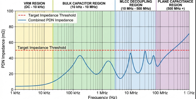
PDN impedance analysis is the process of calculating the impedance "looking into" the PDN from each IC power pin as a function of frequency, usually from DC to 1 GHz or higher. The outcome is a curve of impedance versus frequency – it's a curve that you need to keep below your target impedance at each point. Various PDN elements are responsible for different frequency ranges.
| Frequency Range | Primary PDN Element |
|---|---|
| DC to 1 kHz | Voltage Regulator Module (VRM) |
| 1 kHz to 1 MHz | Bulk decoupling capacitors |
| 1 MHz to 100 MHz | Mid-range ceramic capacitors |
| 100 MHz to 1 GHz | High-frequency ceramic capacitors |
| Above 1 GHz | Power/ground plane capacitance |
Optimizing for decoupling capacitors is not just a matter of "throwing capacitors at the problem. Every real capacitor will have an Equivalent Series Resistance (ESR) and Equivalent Series Inductance (ESL) and thus have a self-resonant frequency (SRF). The capacitor is capacitive below the SRF. Above it, the capacitor turns inductive and actually increases PDN impedance. A well-designed decoupling network will have multiple different capacitor values that will result in overlapping impedance dips that will keep the impedance low throughout the entire bandwidth.
Integration with Signal Integrity Analysis
What a lot of engineers don't realize is this. Signal integrity and power integrity are not distinct issues. They are very interconnected, and you cannot study one without the other because you will only get half the picture. Switching causes a transient inrush current from the PDN. The resulting current draw causes a drop in voltage across the power plane that is local to the current draw and then spreads throughout the power plane, affecting all other ICs on the power plane.
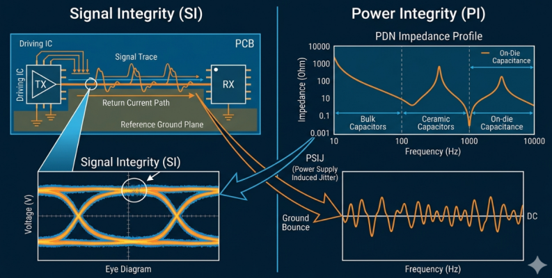
When a sensitive receiver is placed on the same power domain, the noise couples directly into the power pins of the receiver, thus changing the switching threshold. This leads to a smaller noise margin and even to corrupted data. The relationship is bi-directional. Signal return currents run through the ground plane, and if the impedance of the ground plane is not sufficiently low, then the voltage gradients caused by the return currents are manifested as common-mode noise on differential pairs.
Tools and Techniques for Power Integrity Analysis
Popular Power Integrity Analysis Tools and Simulation Methods
Today, there are a number of power integrity analysis tools on the market, from free and readily available to enterprise-grade tools. The selection of choice depends on the level of accuracy required, budget, and design complexity.
| Tool | Vendor | Key Strength | Typical Use Case |
|---|---|---|---|
| PDN Analyzer | Altium | Integrated with Altium Designer, easy DC drop analysis | Mid-complexity boards, quick IR drop checks |
| HyperLynx PI | Siemens EDA | AC impedance analysis, decoupling optimization | High-speed digital, DDR routing |
| Ansys SIwave | Ansys | Full-wave electromagnetic extraction of planes | RF and mmWave power plane analysis |
| Cadence Sigrity | Cadence | Comprehensive PI/SI co-simulation | Enterprise-level server and networking boards |
| SPICE-based tools | Various | Circuit-level PDN modeling with lumped elements | Early-stage design estimation |
| Free online calculators | Saturn PCB, JLCPCB | Quick target impedance and trace width checks | Initial design scoping |
Interpreting Results and Making Design Improvements
Running the simulation is only half the fight! It's in interpreting the results and knowing which design levers to pull that real engineering judgment comes in. If the resonant peak is above the target impedance, the first step in determining the frequency of the peak is to identify it from your impedance plot. If it is in the 1-10 MHz range, adding or moving bulk capacitors (10-47 uF) close to the VRM output generally helps to resolve it. If the peak is in the 50-200 MHz range, then more mid-range MLCC's (100 nF to 1 uF) are needed closer to the IC power pins.
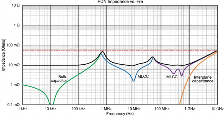
If your high-frequency capacitors have too much mounting inductance or if the power/ground plane spacing is too great, then peaks above 500 MHz are likely to indicate that. When evaluating for DC voltage drop, identify hotspots for current density, copper being forced into a constriction. Typical solutions involve increasing the width of the plane copper in high current areas, adding more vias between the power planes, or increasing the copper weight from 1 oz (35 um) to 2 oz (70 um) in critical areas.
Manufacturing Considerations for Robust Power Delivery
Plane Design and Via Optimization
When designing a power plane, it is important to use continuous copper fills and avoid splits and cutouts. Each slot or split will cause the current to take a detour around the slot or split, thereby increasing the path resistance and inductance. If splits are necessary, use a plethora of stitching vias to keep the low-impedance connections. If you're using multilayer boards, you can reserve whole layers for the power and ground planes that high-frequency decoupling requires.
Optimization for power delivery involves maximizing current-carrying capacity and minimizing inductance. Typical via inductance is 0.5-1.0 nH, and the typical current rating is about 1-1.5 A for a standard 0.3mm drill. To maintain a thermal and inductance budget, you must have an array of at least 8-10 vias for a 10 A power connection between layers. In a via-in-pad design, vias are located within the component pads and are filled with conductive epoxy, which reduces the connection inductance between the IC and the power plane.
JLCPCB's Expertise in Power Integrity Optimized PCBs
Advanced DFM Support for PDN Design
By uploading a power integrity optimized design to JLCPCB, their automated DFM (Design for Manufacturability) review will identify potential problems that may affect your PDN performance. The system highlights copper regions that are narrower than the current loads, indicates possible thermal violations of vias, and checks plane clearances against your design rules.
JLCPCB can provide up to 14 layers of stack-up with controlled dielectric thicknesses for complex multilayer boards that require power integrity. They have an engineering team that can analyze your stackup requirements and suggest laminate combinations to meet interplane spacing requirements as specified by your power integrity analysis. This type of DFM collaboration is particularly beneficial if your design is venturing into 2 oz or greater thicknesses of copper, where processing parameters have to be adjusted.
Reliable High-Performance Manufacturing at Scale
Power integrity isn't just about prototyping. At the point of volume production, you need to have uniformity between all the boards in the batch. JLCPCB process control is designed to keep the copper thickness, dielectric spacing, and quality of the via that your power integrity analysis relies on to be consistent from board 1 to board 100,000.
Their SMT assembly services complement the bare board fabrication, with the positional accuracy required for power integrity, for placement of decoupling capacitors. This is because the decoupling capacitors are not connected in the same location as they are in the real circuit, meaning that extra inductance from mounting the capacitors is not modeled by the simulation and results in poor PDN performance at high frequencies. The pick-and-place accuracy and reflow profile control of JLCPCB guarantee each capacitor is placed precisely where your design calls for it.
FAQ about Power Integrity Analysis
Q: What is power integrity analysis in PCB design?
Power integrity analysis is the process of evaluating and optimizing the power distribution network (PDN) on a PCB to ensure that all integrated circuits receive clean, stable voltage within their specified tolerances. It involves modeling the impedance of power and ground planes, decoupling capacitors, vias, and traces across a wide frequency range.
Q: How does power integrity analysis differ from signal integrity analysis?
Signal integrity analysis focuses on the quality of individual signal waveforms as they travel along traces, examining reflections, crosstalk, and losses. Power integrity analysis focuses on the quality of the voltage supply delivered to ICs through the power distribution network.
Q: What tools are commonly used for power integrity analysis?
Popular power integrity analysis tools include Altium PDN Analyzer for DC drop analysis, Siemens HyperLynx PI for AC impedance analysis, Ansys SIwave for full-wave electromagnetic extraction, and Cadence Sigrity for comprehensive PI/SI co-simulation.
Q: How does copper thickness affect power delivery on a PCB?
Copper thickness directly determines the DC resistance of power planes and traces. Standard 1 oz (35 um) copper has a sheet resistance of approximately 0.5 milliohms per square. Doubling to 2 oz copper halves this resistance, reducing IR voltage drops proportionally.
Conclusion
Power integrity analysis has become essential for modern high-performance PCBs. With lower voltages and higher currents, maintaining a stable PDN is critical to prevent voltage droop, ground bounce, and signal integrity issues.
By properly designing decoupling networks, optimizing power/ground planes, and minimizing inductance, you can ensure reliable power delivery to demanding ICs. Combining thorough PI analysis with professional manufacturing guarantees your design performs as simulated.Ready to build stable power delivery? Upload your PCB design to JLCPCB today.
Popular Articles
Keep Learning
Optimizing Power Nets for Stable and Efficient High-Performance PCBs
Key Takeaways Power Nets as Systems: It is a complete copper network of planes, pours, traces, and vias built to deliver clean, stable voltage. Control IR Drop: Copper resistance causes voltage drop. Use wider traces, solid pours, or heavier copper (2 oz+) to stay within voltage tolerances. Minimize Loop Area: Place decoupling capacitors close to power pins with short, wide traces to handle fast transient currents. Scale Your Vias: A single 0.3mm via carries only 1 to 2A. High-current paths require pa......
Achieving Stable Power Delivery : Mastering PDN Impedance in High-Performance PCBs
Key Takeaways PDN impedance directly determines voltage stability under load. Keep it low and flat. Calculate your target: Z_target = (V_dd × Ripple%) / I_transient — typically single-digit milliohms. Prioritize close power-ground planes, short via connections, and strategic decoupling placement. Avoid anti-resonance peaks; a smooth curve matters more than raw capacitance. Precise manufacturing (copper thickness, dielectric control) is essential to match simulation results. There's no point in using a......
Phase Matching in High-Speed PCB Design: Achieving Signal Integrity with Precision Manufacturing
Key Takeaways Phase matching controls electrical trace length in high-speed PCBs to maintain precise signal timing and phase relationships. Even 10–15 ps skew (roughly 1–2 mm difference) at 10 Gbps can collapse eye diagrams, raise bit error rates, and cause system failures. Dynamic phase matching maintains alignment throughout the entire signal path, accounting for bends, vias, and layer transitions. USB 3.x SuperSpeed interfaces commonly target intra-pair skew below 5 mils (0.13 mm) to maintain relia......
Mastering Split Planes for Cleaner Power Delivery and Better Signal Integrity
Key Takeaways Split power planes when needed for multiple voltage domains or analog/digital isolation, but never split ground planes — always keep ground continuous for clean return paths. Avoid routing high-speed signals across splits; if unavoidable, use stitching capacitors (0.1 µF) and ensure differential pairs cross together. Place split power planes next to a solid ground layer, maintain ~10 mil moat width, and use proper decoupling near IC pins. Good split plane design significantly reduces noi......
Building Stable Power Delivery for High-Performance PCBs with Power Integrity Analysis
Key Takeaways Power integrity analysis is essential for building stable power delivery in high-performance PCBs. By maintaining low PDN impedance, optimizing decoupling capacitors, and designing robust power/ground planes with minimal voltage droop and inductance, engineers can prevent common failures such as voltage droop, ground bounce, and power-induced jitter. Combining thorough PI simulation with smart layout practices and professional manufacturing ensures reliable performance from prototype to ......
How Impedance Controlled Routing Delivers Reliable High-Speed PCB Performance
Key Takeaways Impedance Controlled Routing is essential for reliable high-speed PCB performance above 1 Gbps, eliminating reflections, ringing, and bit errors by precisely targeting interface-specific impedances (USB 90 Ω, PCIe 85 Ω, DDR4 40/80 Ω, HDMI 100 Ω) through field-solver calculations, symmetrical stackups with continuous reference planes, stable low-loss dielectrics, and strict single-ended/differential routing rules. Manufacturing precision in etching, copper profile, and lamination, verifie......