Flex PCB Manufacturers for Compact Electronics: Sourcing Guide
17 min
- Why Compact Electronics Require Specialized Flex PCB Manufacturing
- Choosing the Right Flex PCB Architecture for Small Devices
- Engineering and DFM Guidelines for Compact Flex PCB Design
- Flex PCB Materials and Stackups for High-Density Circuits
- Flex PCB Manufacturing Process for Miniature Electronics
- Flex PCB Applications in Compact Electronics
- How to Evaluate Flex PCB Manufacturers for Compact Electronics
- JLCPCB Flex PCB Manufacturing Capabilities for Compact Devices
- Conclusion
- FAQs About Flex PCB Manufacturing for Compact Electronics
When choosing a flex PCB manufacturer for your compact electronics application, be sure to consider not only their maximum trace density, maximum stackup thickness, maximum bend radius, and stiffener thickness, but also whether they routinely build such parts. Since a design based on the manufacturer's best-case fabrication limits may be very tight in terms of production yield and/or dimensional tolerances, and long-term reliability, particularly in compact devices where space may be limited and repeated bending may be required.
This guide will take you through the impact of compact electronic devices on flexible PCB architecture, stackup design, and bend-radius selection. You'll also learn the design rules and materials to use for dense, thin, and repeatedly flexed circuits, the manufacturing process (including costs) of small flexible PCBs, and what to check, ask, and send to a flex PCB manufacturer when considering them for your project.
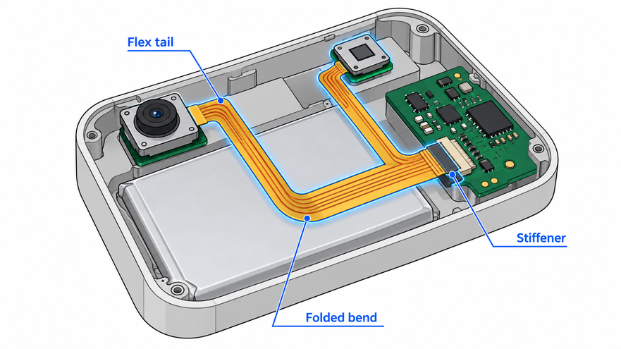
Figure: Thin flex circuit folded around a battery, a camera, and modules inside a compact enclosure
Why Compact Electronics Require Specialized Flex PCB Manufacturing
Compact electronics require flex PCB manufacturing because a flexible circuit can replace cables and connectors, fold in three dimensions, and fit in enclosures that cannot accommodate a flat rigid board. Those advantages rely on thin materials and small features, and fabricators vary in which of those they create at production yield.
Replacing Wire Harnesses, Connectors, and Rigid Interconnects
A flex circuit is a single thin, laminated component with a number of conductors that alters the interconnect budget for a small device:
- Less volume: One flex tail replaces a wire bundle and its two mating connectors.
- Lower weight: Thin film and copper weigh less than insulated wire and connector housings.
- Fewer assembly steps: One laminated part replaces hand-routed wires and crimped terminations.
- Fewer contact interfaces: Each removed connector removes a mated contact pair that can loosen or corrode.
A flex circuit does not always cost less than a harness. The savings depend on volume, assembly labor, and the number of connectors the design removes.
Enabling 3D Packaging, Folding, and Irregular Enclosure Designs
Flex circuits can be folded around a battery, behind a camera module, across a hinge, or around a curved housing wall. If the circuit bends only once when the device is assembled, a different stackup is required than if it bends every time the hinge is opened.
Flex PCB vs. Rigid PCB vs. Rigid-Flex PCB for Miniaturization
Every type of board addresses a unique packaging issue:
| Property | Rigid PCB | Flex PCB | Rigid-Flex PCB |
| Typical thickness | Thicker, self-supporting | Thinnest of the three | Rigid in board sections, thin in flex sections |
| Flexibility | None | Static or dynamic bending | Flexible sections only |
| Mechanical support | Built in | Stiffeners were needed | Built into rigid sections |
| Assembly complexity | Lowest | Needs carriers or fixtures | Highest; fewer separate interconnects |
| Typical use | Main logic and power boards | Interconnects, sensors, wearables | Multi-board assemblies with fewer connectors |
Choosing the Right Flex PCB Architecture for Small Devices
The optimum flex PCB design is the minimum number of copper layers necessary to provide the routing, and a stackup thin enough for the desired flex.
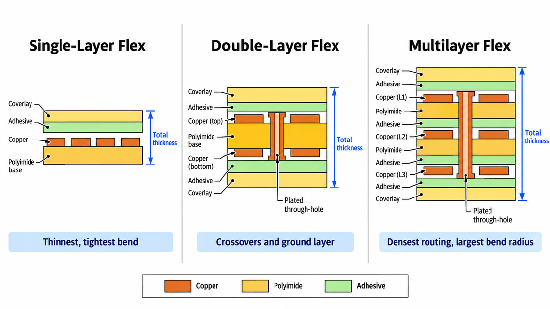
Figure: Flex PCB architecture cross-sections for single-layer, double-layer, and multilayer compact flexible circuits.
Single-Layer, Double-Layer, and Multilayer Flex Circuits
- Single-layer flex: One layer of copper between base film and coverlay. The thinnest construction can be placed near the neutral axis and is therefore well-suited for tight and dynamic bends.
- Double-layer flex: Copper on both sides of the base film, with plated holes. Crossovers and a ground layer are possible, but very thick.
- Multilayer flex: Three or more layers of copper. It is the thickest and stiffest, with dense routing, but requires the largest bend radius.
Static Flex vs. Dynamic Flex: Designing for the Actual Movement
A static flex circuit is bent during installation and then fixed. A dynamic flex circuit flexes many times during use, such as a hinge or a moving print head. For a static design, the fabricator's thickness and bend information is required. A good flex design must also have a defined number of cycles, appropriate materials that can withstand flex fatigue, and bend-test data.
Balancing Miniaturization, Routing Density, and Mechanical Reliability
There is a trade-off between mechanical endurance and density when shrinking a flex circuit. The closer the traces are to the narrow ends where tears begin, the narrower the tails will be, and the higher the number of layers, the smaller the minimum bend radius. The flex PCB design guide suggests placing vias, pads, and dense copper areas in static areas, which are out of the bend.
| Device Type | Typical Movement | Suggested Architecture |
| Wearable band or smart ring | Installed curve, occasional flexing | Single-layer or double-layer with thin copper |
| Hinge or foldable link | Repeated dynamic bending | Single-layer in the bend zone |
| Camera or sensor module | Static fold during assembly | Double-layer, stiffened at the connector |
| Dense module interconnect | Static fold | Multilayer, with fewer layers through the bend |
Engineering and DFM Guidelines for Compact Flex PCB Design
Compact flex design guidelines ensure that fine features are within the fabricator's regular capabilities, and that holes, pads, and stiffness changes are outside the bend area.
High-Density Routing: Fine Traces, Spacing, Teardrops, and Staggered Conductors
Thinner copper has minimum trace widths and spacing, as there is less time for the copper to be etched and less undercutting. Design to the regular value and keep the absolute limit as a backup, as it reduces yield and may increase cost. In flexible areas:
- Teardrops: Add teardrops at junctions between pad and trace and at junctions between via and trace to distribute stress.
- Curved traces: Use arcs instead of 90° corners, as corners strain the focus.
- Staggered conductors: Traces on alternate layers are offset from each other and do not form a stiffer I-beam.
- Hatched copper: Reduce stiffness by using hatched instead of solid copper in flexible areas.
Calculating Bend Radius and Understanding Neutral-Axis Stress
The bend radius is specified as a multiple of the total circuit thickness, and at the inside bend surface. According to just two of the sources published by JLCPCB, the multipliers are as follows:
- Minimum (capabilities page): 6× thickness single layer, 10× thickness multilayer, 10-15× thickness dynamic bend.
- Conservative (flexible PCB bend radius guide): 6× (single-layer or static bend), 12× (multilayer or static bend), 100× (single-layer or dynamic bend), 100-150× (multi-layer or dynamic bend).
Assume the capabilities numbers are the minimum values for a static bend. Use the conservative multipliers as a starting point for any dynamic or cycled bend and validate using a bend-cycle test on prototypes. Bending strain in a conductor is of the order of ε ≈ y / R, where y is the distance of the conductor from the neutral axis and R is the radius to the neutral axis.
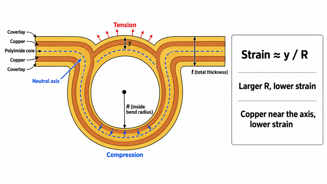
Figure: Flex PCB bend radius measured at the inside surface
Via Placement, Pad Reinforcement, and Bend-Zone Keep-Outs
Generally, plated holes, exposed pads, solder joints, and sudden changes of stiffness should not be located in the active bend area:
- Vias and plated holes: At least 1.0 mm from the bend-zone boundary is recommended for static bends, and 1.5 mm for dynamic bends.
- Pads: Anchor pads in flexible areas with coverlay overlap, and teardrop their trace entries.
- Stiffener edges: Stiffen an edge not along the bend line so that stiffness is not applied in the fold.
Connector Footprints, Gold Fingers, and Stiffener Placement
A ZIF requires the flex tail to be made to the thickness specified in the datasheet, typically achieved by placing a PI stiffener behind the gold fingers.
- Finger thickness: Circuit thickness plus stiffener plus stiffener-bonding adhesive equals the thickness listed in the dconnector datasheet. JLCPCB gives a calculator for the PI thickness of gold-finger tails.
- Pad support: Use a stiffener on the back of SMT connectors to prevent solder joints from bending under load.
- Edge support: Take the stiffener to the edge of the coverlay at the finger roots to prevent the copper from flexing there.
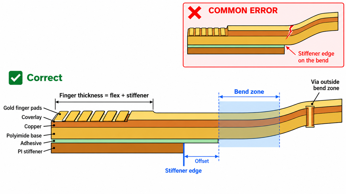
Figure: Flex PCB connector tail with a PI stiffener behind the gold fingers and a stiffener edge offset from the bend zone.
Flex PCB Materials and Stackups for High-Density Circuits
When designing a compact circuit, the first selection of flex PCB materials is based on the thickness and bend life of the laminate's four key components: copper foil, protective layer, and stiffener. The flex PCB stackup design guide illustrates how they sum up.
Adhesiveless vs. Adhesive-Based Polyimide Laminates
Flexible copper-clad laminate (FCCL) bonds copper to polyimide in one of two ways:
- Adhesiveless FCCL: Copper bonded directly to polyimide. It is thinner, more dimensionally stable, and better for repeated bending and dense, thin stackups.
- Adhesive-based FCCL: Copper bonded with an acrylic or epoxy adhesive layer. It costs less and suits many static designs, but the adhesive adds thickness.
Laminate adhesive is separate from coverlay adhesive, so an adhesiveless design can still have adhesive under its coverlay.
Rolled-Annealed vs. Electrodeposited Copper
Copper foil type sets fatigue life in the bend:
- Rolled-annealed (RA) copper: Better fatigue resistance under repeated bending, at a higher price. It is the usual choice for dynamic flex.
- Electrodeposited (ED) copper: Lower cost, good conductivity, and suitable for static bends. Standard ED foil tolerates fewer bend cycles.
Common flex copper weights are 1/3 oz (12 µm), 1/2 oz (18 µm), and 1 oz (35 µm). Thinner copper lowers bending strain and allows finer traces. Thinner foils, such as 1/4 oz, are supplier-dependent, and foil type is not always stated, so confirm both with the manufacturer.
Polyimide Film Coverlay vs. Photoimageable Protective Coatings
Flex circuits have three protective layers; each has a different mechanical limit:
- Polyimide film coverlay: Polyimide film with adhesive on top of the circuit. It has good resistance to repeated bending, but its pre-cut holes do not align as accurately and are therefore not ideal for very fine-pitch pads.
- Photoimageable covercoat: A flexible coating that is patterned by exposure and development. Provides more restriction and less bendability than film coverlay.
- Flexible solder mask: A liquid photoimageable mask for fine-pitch areas that are stiffened and/or static. May fracture in an area of high flex.
A typical compact design is one in which the bend is covered with a film coverlay, and the photoimageable layer is used only where fine-pitch pads are required. Check with the manufacturer what they offer from the three.
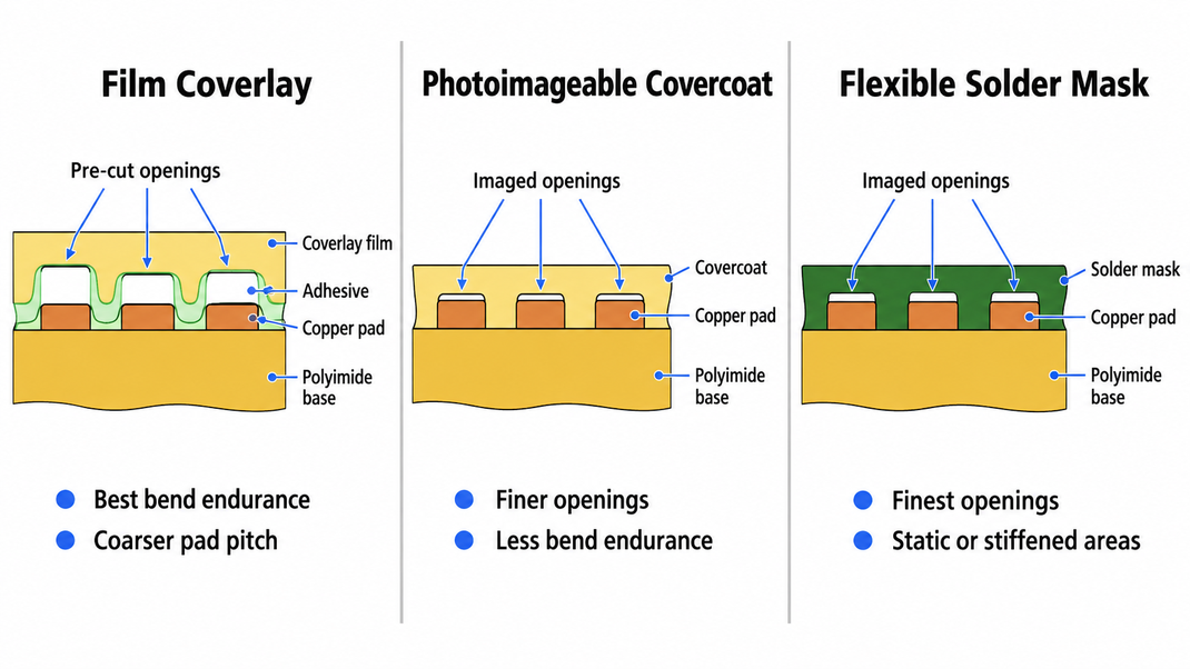
Figure: Flex PCB materials compared: film coverlay, photoimageable covercoat, and flexible solder mask over fine-pitch pads.
PI, FR4, and Stainless Steel Micro-Stiffeners
Stiffener choice trades added height against flatness and cost:
| Stiffener | Benefit | Limitation | Recommended Use |
| Polyimide (PI) | Thin, sets precise finger thickness | Limited flatness support | ZIF and gold-finger connector tails |
| FR4 | Rigid, low cost, takes through-hole parts | Thicker edges can chip | Through-hole parts and connector backs |
| Stainless steel | High flatness at low thickness | Can be magnetic, depending on grade | Flat support under SMT components |
Keep steel stiffeners away from Hall-effect and other magnetically sensitive sensors. The FPC stiffener and EMI guide lists the thicknesses and layer names for each material.
Flex PCB Manufacturing Process for Miniature Electronics
The flex PCB manufacturing process builds the circuit on film, protects it, adds support, and cuts it out. For miniature parts, dimensional stability and registration matter at each step, because small pads leave little alignment margin.
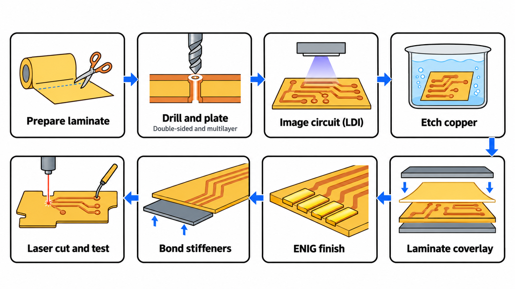
Figure: Flex PCB manufacturing process for miniature electronics
Material Preparation, Imaging, Etching, and Plating
- Prepare the laminate: Cut FCCL sheets and bake them to remove moisture.
- Drill and plate: On double-sided and multilayer builds, drill the holes, then metalize and plate them.
- Imagine the circuit: Expose dry-film resist, often via laser direct imaging (LDI), with a scale offset to compensate for the film's dimensional changes due to heat and moisture.
- Etch: Remove the unprotected copper and strip the resist.
Coverlay Lamination, Stiffener Bonding, Surface Finishing, and Cutting
Coverlay openings are cut and heat- and pressure-laminated to the pads. Flows a little bit into each opening, openings are larger than the pad. Stiffener bonding then sets the final connector thickness and surface finish, usually ENIG on flex, plating the exposed copper.
- UV laser cutting: No cutting die required; follow the CAM outline; tight tolerances; suitable for prototype and small-batch production of complex-shaped parts.
- Mechanical die cutting: A part outline die and tooling are required, but it cuts faster per part at high volume.
Final Inspection, Electrical Testing, and Production Yield
- AOI: Optical inspection finds opens, shorts, and width errors on each layer.
- Electrical test: Flying-probe or fixture testing confirms continuity and isolation.
- Dimensional inspection: Checks outline, finger thickness, and coverlay registration.
- Defect checks: Visual and microsection checks look for delamination, voids, and plating defects.
Production yield is higher when fine features sit at regular limits rather than at the extremes.
Flex PCB Applications in Compact Electronics
Flex PCB applications in compact electronics share three demands: thin stackups, tight bends, and small connector areas. They differ in how often the circuit moves and where it operates.
| Application | Compact-Design Demand | Requirement to Specify |
| Wearables and smart rings | Curved housings, thin tails | Thinnest stackup, PI stiffener at connectors |
| Foldable electronics | Repeated hinge bending | Dynamic flex, RA copper, cycle test |
| Endoscopes and miniature cameras | Narrow interconnects, fine-pitch parts | Fine trace/space, tight outline tolerance |
| Automotive cameras | Vibration and temperature | Operating range, stiffened connectors |
| Industrial sensors and IoT | Small size, connector limits | Standard stackup, panel efficiency |
How to Evaluate Flex PCB Manufacturers for Compact Electronics
Evaluate flex PCB manufacturers for compact electronics by comparing their published regular limits with your design, then asking for evidence of stackup control, quality testing, and scalable production. Compare the price after those checks.
Verify Minimum Trace, Hole, Outline, and Thickness Capabilities
Separate each capability table into regular and extreme or custom limits, then check:
- Trace and space: At your copper thickness, not at the thinnest foil listed.
- Hole and pad size: Including whether small holes are mechanically or laser drilled.
- Finished thickness: The listed stackup options and their tolerances.
- Outline tolerance: Standard and on-request values for laser cutting.
Discuss a design that needs extreme values for several features with the fabricator before ordering.
Quality Assurance, IPC Requirements, and Flex Endurance Testing
Two IPC documents frame flex quality:
- IPC-2223: The sectional design standard for flexible and rigid-flex boards.
- IPC-6013: The qualification and performance specification for flexible and rigid-flex boards, with Class 1, 2, and 3 requirements.
The class is scheduled in the purchase documents. Check his fabricator's certification class and ask about the class they fabricate and inspect. MIT folding endurance (ASTM D2176) is a method to fold a specimen of material until it breaks. IPC-TM-650 flexural fatigue procedures are used to test conductor patterns in coupons. Neither is a substitute for testing your circuit at its actual bend radius.
Manufacturer Selection Checklist: Questions to Ask Before Ordering
- Capabilities: What are the regular and extreme trace, hole, and outline limits?
- Stackups: Which stackups are offered, and what is the finished thickness tolerance?
- Bending: Can the stackup meet the required bend radius and expected flex cycles?
- Support: Which stiffener materials and connector-finger thicknesses are available?
- Quality: Which IPC class applies, and what test evidence is supplied?
- Commercial: How do sample approval, lead time, pricing, and capacity change from prototype to volume?
JLCPCB Flex PCB Manufacturing Capabilities for Compact Devices
The following values are the most important ones for compact devices: 0.07 mm single-layer stackup, 3/3 mil traces on 12 µm copper, ±0.1 mm laser-cut outlines, PI, FR4, or stainless steel stiffeners. These are the values published by the vendors, and options may vary depending on the construction ordered.
Miniature Flex PCB Capability Matrix
Values from the JLCPCB flex PCB capabilities page:
| Specification | JLCPCB Capability | Why It Matters for Compact Devices |
| Layer count | 1, 2, and 4 layers; rigid-flex not supported | Multi-board designs use flex tails and connectors instead of rigid-flex |
| Thinnest finished stackup | 0.07 mm single-layer; 2-layer from 0.11 mm; 4-layer 0.20–0.45 mm | Thickness sets the minimum bend radius and the connector-tail height |
| Base film | Polyimide, 25 or 50 µm; transparent PET, 36 µm | 25 µm polyimide gives the thinnest stackups |
| Copper thickness | 12, 18, or 35 µm (2- and 4-layer); 18 or 35 µm (single-layer) | 12 µm copper allows the finest traces and lowers the bending strain |
| Trace/space | 3/3 mil on 12 µm copper; 2/2 mil absolute limit | Route dense fan-outs at 3/3 mil and keep 2/2 mil in reserve |
| Via hole/pad | 0.3/0.55 mm regular; 0.10/0.30 mm (2-layer) at extra cost | Smaller vias save area but add cost, and stay outside the bend |
| Surface finish | ENIG, 1 or 2 µin gold | Flat pads suit fine-pitch parts and gold fingers |
| Stiffeners | PI, FR4, stainless steel, adhesive tape; EMI shielding film | Set connector-finger thickness and flat SMT support |
| Outline tolerance | Laser cut, ±0.1 mm; ±0.05 mm on request | Controls fit in tight enclosures, and the width of ZIF tails |
| Board size | Up to 234 × 490 mm; panelize boards under 20 × 20 mm | Very small circuits are ordered as panels |
| Impedance | Not controlled; reference trace widths provided | High-speed tails need their own stackup verification |
Conclusion
The best flex PCB manufacturers for compact electronics are those with standard limits for trace density, stackup thickness, bend requirements, and stiffener requirements, with margin for your design. Select the supplier with published capabilities and test evidence consistent with your geometry, and verify fit and bending on prototypes before scaling. That ensures that a miniature design can be fabricated at production yield. When your files are ready, upload them for a flex PCB quote.
FAQs About Flex PCB Manufacturing for Compact Electronics
Q. How Thin Can a Custom Flex PCB Be Manufactured for a Compact Electronic Device?
Ans: A single-layer circuit on 25 µm polyimide can finish below 0.1 mm; JLCPCB lists 0.07 mm. Stiffeners add thickness, and copper-free areas are thinner, so specify the required thickness for each controlled area.
Q. What Is the Minimum Bend Radius for Single-Layer and Multilayer Flex PCBs?
Ans: For static bends, JLCPCB publishes 6× total thickness for single-layer and 10–12× for multilayer flex. Dynamic bends need 10–15× to 100–150×, depending on the source, so confirm the radius with prototype bend tests.
Which Flex PCB Materials Are Best for Repeated Bending?
Ans: Rolled-annealed copper on adhesiveless polyimide, with the thinnest copper the current allows and film coverlay across the bend, gives the longest bend life. Keep one copper layer in the bend, near the neutral axis.
Q. When Should a Compact Design Use PI, FR4, or Stainless Steel Stiffeners?
Ans: Use PI to set gold-finger thickness for ZIF connectors, FR4 behind through-hole parts and connector bodies, and stainless steel where thin SMT areas must stay flat. Avoid steel near magnetic sensors and check the total height against the enclosure.
Q. How Do Minimum Trace Width and Hole Size Affect Flex PCB Manufacturing Cost?
Ans: Features at a fabricator's regular limits are priced as standard. Features at the extreme limits yield lower yields, may require slower processes, and often carry a surcharge, so reserve them for routing that needs them.
Keep Learning
Flex PCB Manufacturers for Compact Electronics: Sourcing Guide
When choosing a flex PCB manufacturer for your compact electronics application, be sure to consider not only their maximum trace density, maximum stackup thickness, maximum bend radius, and stiffener thickness, but also whether they routinely build such parts. Since a design based on the manufacturer's best-case fabrication limits may be very tight in terms of production yield and/or dimensional tolerances, and long-term reliability, particularly in compact devices where space may be limited and repea......
Quick Turn PCB: How to Get High-Quality Prototypes Fast
Printed Circuit Boards (PCBs) are a vital part of modern electronics, and the demand for faster and more efficient development made a quick turn PCB services extremly important. In this article, we will discuss what quick turn PCB is, its importance, the lead time for JLCPCB's quickturn PCB fabrication, how quick turn PCB can help businesses, and how to choose a good quick turn PCB manufacturer. What is Quick Turn PCB? Quick turn PCB refers to the process of manufacturing and delivering PCBs within a ......
7 Must-Know Tips for Choosing the Right Flex PCB Supplier
Flexible PCBs provide immense design and engineering benefits thanks to their versatility. But to maximize their value, having the right manufacturing partner makes all the difference. Choose wisely, and you will be well-positioned to capitalize on the advantages of flex PCB technology for your application. This article provides a step-by-step guide to evaluating and selecting an optimal flexible PCB maker based on their competencies, quality control, materials, pricing, capacity and more. By approach......
How to Build a Bulletproof Bill of Materials for Flawless PCB Production
Have you ever sent a PCB design to be assembled only to receive an email requesting why you have not provided a part number or the package has not been matched? In that case, you are already aware that a single slip in your bill of materials will bring a flawless board down. Take a small CH32V003-based dev board consisting of 29 components distributed on 11 different footprints on a 2-layer copper PCB. It has an MCU, USB-C input, 24MHz crystal, USB-to-TTL bridge, indicator LEDs, and programming/GPIO h......
The True Cost of Custom PCBs: Understanding the Factors that Affect the Bottom Line
Key Takeaways Optimize Layout & Size: Simplify circuit design and keep board size within 100mm x 100mm for basic promo rates. Stick to Standard Specs: Use 1.6mm board thickness and 1 oz copper weight to avoid material surcharges. Respect DFM Limits: Maintain trace width/spacing ≥ 5/5 mil and via drills ≥ 0.3mm to prevent fine-feature fees. Select Low-Cost Finishes: Choose HASL over ENIG for prototypes unless fine-pitch BGAs are required. Printed circuit boards (PCBs) are integral to modern technology,......
Crafting Success: Choosing the Right PCB Manufacturer for Hobbyist
As a PCB hobbyist or engineer, finding a reliable and professional PCB manufacturer is crucial to ensure the success of your projects. The right PCB manufacturer can provide you with valuable guidance, access to advanced manufacturing technologies, and the support needed to excel in the dynamic world of PCB design and manufacturing. In this article, we will explore key characteristics to consider when selecting a PCB manufacturer, with a focus on professional instruction, customization options, qualit......