
What Is a BGA Chip? A Complete Guide to Ball Grid Array Packaging
16 min
- What is a BGA Chip?
- Internal Structure of a BGA Chip Package
- How a Ball Grid Array Package Works
- Common Types of BGA Packages
- Key Advantages of Using a BGA Chip
- Common Challenges and Limitations of BGA Chips
- Applications of BGA Chips
- BGA vs QFP vs LGA Packages
- PCB Layout and Pad Design for BGA Chips
- BGA Chip Assembly and Inspection
- Reliable BGA PCB Assembly with JLCPCB
- FAQs
- Conclusion
Modern electronics require compact packages with high connection density and efficient heat dissipation. Ball Grid Array (BGA) technology has become a key solution for high-performance PCB design.
Because of these advantages, BGA chips are widely used in processors, graphics devices, memory modules, networking hardware, and compact embedded systems.
This guide explains how BGA packages work, the common types available, their key benefits and challenges, and the essential PCB design and assembly considerations for reliable manufacturing.
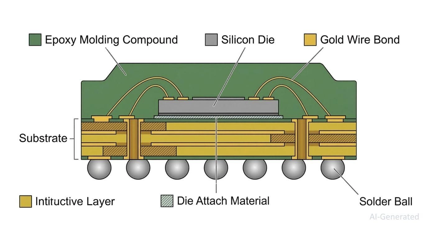
Figure: A BGA chip showing the silicon die, gold wire bonds, substrate, and bottom solder balls.
What is a BGA Chip?
A BGA chip (Ball Grid Array chip) is a type of surface-mount integrated circuit package that uses an array of small solder balls on the underside of the device to create electrical and mechanical connections with a printed circuit board (PCB).
Unlike traditional leaded packages such as Quad Flat Package (QFP), which place fragile metal leads around the perimeter, BGA packaging distributes connections across the entire bottom surface of the component. This design enables much higher pin density, improved electrical performance, and better heat dissipation, making BGA chips ideal for high-performance and high-density electronic systems.
Because of their compact footprint and superior signal integrity, BGA chips are widely used in processors, GPUs, memory devices, networking ICs, and advanced embedded systems where traditional packages cannot meet modern performance and miniaturization demands.
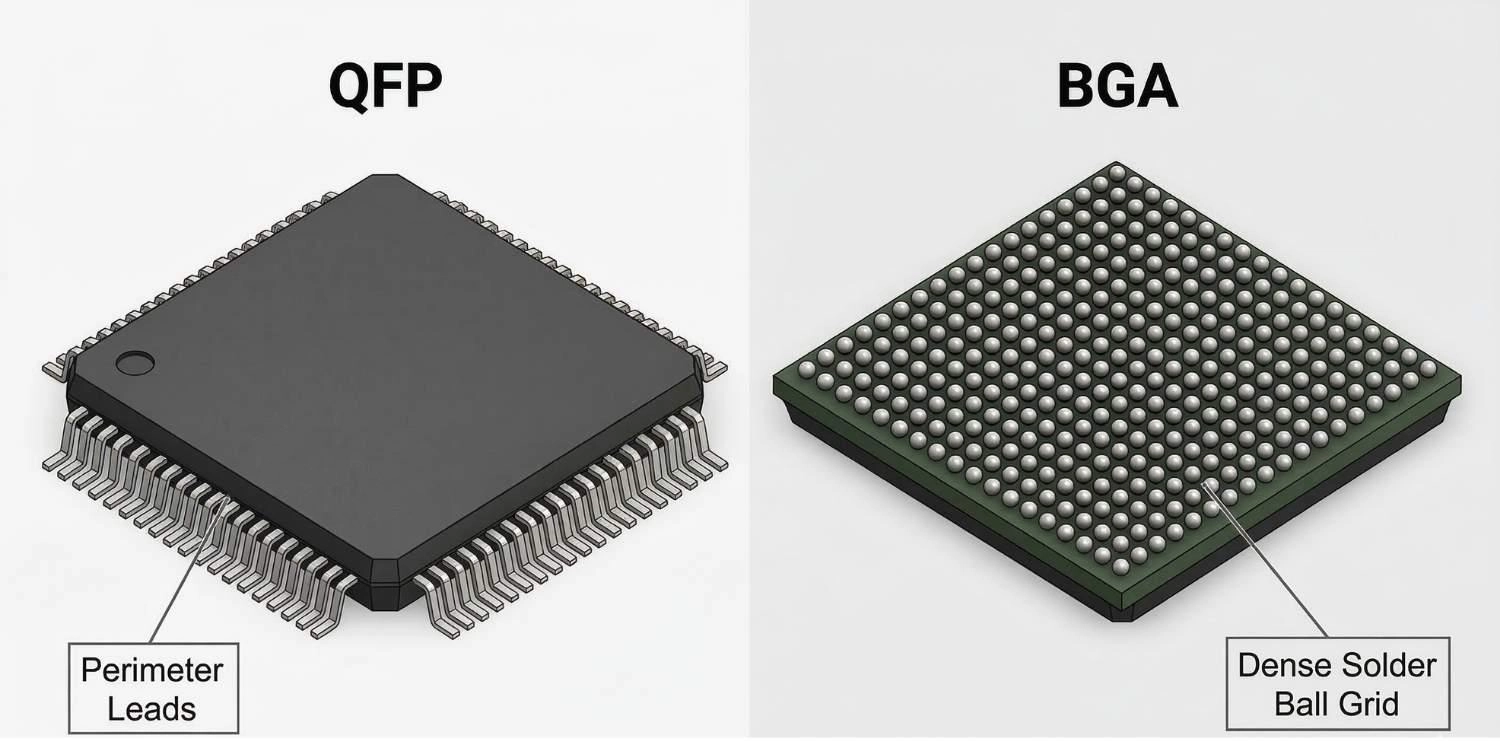
Figure: 3D isometric comparison showing a Quad Flat Package with perimeter leads next to a Ball Grid Array chip with bottom solder balls.
Internal Structure of a BGA Chip Package
To understand how a BGA chip operates, it is essential to examine its internal package structure. A BGA package consists of multiple engineered layers that connect the microscopic silicon die to the printed circuit board while ensuring electrical performance, thermal dissipation, and mechanical reliability.
Semiconductor Die
The semiconductor die is the active silicon component where signal processing and logic operations occur. It is also the primary source of heat generation inside the package. In standard wire-bonded packages, the die is mechanically secured to the substrate using a specialized Die Attach Film (DAF) or conductive epoxy, which keeps the silicon firmly in place.
Interconnection Layer (Wire Bond or Flip-Chip)
This is a critical layer that packaging engineers focus on heavily, as it bridges the die to the package substrate. In traditional BGA designs, ultra-fine gold or copper wires are used (wire bonding) to connect the die's top perimeter pads to the substrate. In advanced, high-performance chips, the die is flipped upside down and attached directly to the substrate using microscopic solder bumps (flip-chip technology). This drastically reduces the signal path length and electrical inductance.
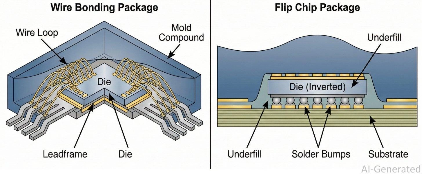
Figure: Cross-section comparison showing standard wire-bond internal connections versus advanced flip-chip BGA micro-bump connections.
Package Substrate
Acting as an intermediary, this is essentially a miniature, multi-layer organic or ceramic PCB inside the chip. It performs signal redistribution, taking the ultra-dense, microscopic connections from the interconnection layer and "fanning them out" to match the wider grid of the external solder balls. Advanced substrates utilize laser-drilled microvias to efficiently route complex signals from the top mounting pads down to the bottom without signal degradation. It also contains dedicated internal power and ground planes to ensure clean power delivery to the die.
Solder Ball Array
Located at the very bottom, this is the grid of spherical solder contacts that will eventually mate with your main PCB. Engineers must carefully specify the ball pitch (the distance between ball centers, commonly ranging from 1.0mm down to a microscopic 0.4mm) and the specific metallurgy (such as SAC305 lead-free solder) to guarantee long-term mechanical reliability and strong electrical conductivity after reflow. The solder balls also provide stand-off height between the package and PCB, improving stress distribution and thermal fatigue resistance.
Encapsulation and Underfill
To protect the delicate die and microscopic wire bonds from physical damage, moisture ingress, and oxidation, the top portion is covered in a hardened epoxy mold compound. In high-performance flip-chip designs (FCBGA), an underfill epoxy is additionally injected into the microscopic gap between the die and the substrate. The underfill distributes thermal-mechanical stress and prevents flip-chip micro-bump fatigue during repeated temperature cycling.
How a Ball Grid Array Package Works
A Ball Grid Array (BGA) package connects an integrated circuit to a printed circuit board using an array of solder balls arranged in a grid on the underside of the device. Each solder ball aligns with a corresponding PCB pad, enabling high-density electrical connections in a compact footprint.
Inside the package, the silicon die is mounted on a multilayer substrate that routes signals and power to the external solder balls. Electrical connections are formed using fine wire bonding or flip-chip interconnects, depending on performance requirements.
During PCB assembly, the BGA component is placed onto solder-pasted pads and heated in a controlled reflow process. As the solder melts, surface tension helps the package self-align, forming strong electrical, mechanical, and thermal joints. This connection method provides shorter signal paths, lower parasitic inductance, and improved heat dissipation compared with traditional leaded packages.
Common Types of BGA Packages
Not all BGA chips are created equal. Depending on the thermal dissipation requirements, electrical speed, and operating environment of your project, the substrate material of the BGA will vary. If you are exploring various BGA package types for your next BOM, these are the most common variations:
PBGA (Plastic Ball Grid Array)
The Plastic BGA is the most widely used package in standard consumer electronics, microcontrollers, and memory modules. It utilizes a plastic-coated bismaleimide triazine (BT) resin substrate. It offers a great balance of cost-effectiveness and reliable electrical performance, though its thermal conductivity is moderate compared to other types.
CBGA (Ceramic Ball Grid Array)
For telecommunications, aerospace, and high-temperature industrial environments, Ceramic BGAs are the standard. The ceramic substrate provides exceptional electrical insulation and vastly superior thermal conductivity, allowing the chip to operate reliably under extreme stress without degrading.
TBGA (Tape Ball Grid Array)
Tape BGAs use a flexible polyimide tape as the substrate. This allows the package to be exceptionally thin. TBGAs offer excellent heat dissipation (often paired with a custom heat sink) and are ideal for ultra-thin laptops and high-end processors where vertical space is heavily constrained.
FCBGA (Flip Chip BGA)
In an FCBGA, the silicon die is flipped upside down and directly attached to the substrate using micro-bumps, eliminating the need for wire bonds. This creates the shortest possible electrical path, drastically minimizing inductance and signal delay. FCBGAs are universally used for high-speed GPUs, CPUs, and advanced networking silicon.
BGA Type | Substrate Material | Thermal Performance | Typical Applications | Cost |
|---|---|---|---|---|
PBGA | BT Resin / Plastic | Moderate | Microcontrollers, RAM, Consumer Tech | Low |
CBGA | Ceramic | Excellent | Aerospace, Telecom, Automotive | High |
TBGA | Polyimide Tape | Very Good | Ultra-thin laptops, Mobile devices | Medium |
FCBGA | Flip-Chip / Resin | Excellent | CPUs, GPUs, High-speed processing | High |
Key Advantages of Using a BGA Chip
The transition to BGA packaging isn't just about saving space; it offers profound electrical and mechanical benefits that drive modern computing.
High Pin Density (I/O Count)
By utilizing the entire bottom surface area of the chip rather than just the perimeter, BGAs can easily accommodate hundreds or even thousands of I/O connections in a footprint a fraction of the size of an equivalent QFP.
Superior Thermal Conduction
Heat is the enemy of processing power. In a BGA chip, heat generated by the silicon die travels straight down through the substrate and solder balls, dispersing directly into the PCB's internal copper ground planes. This makes the PCB itself act as a highly efficient heat sink.
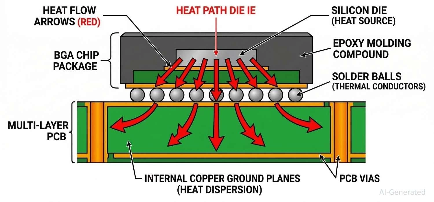
Figure: Illustrating heat dissipating from a BGA silicon die down through solder balls into the PCB copper ground planes.
Lower Inductance and Better Electrical Performance
The spherical solder balls provide a much shorter path between the chip and the PCB than traditional wire leads. This short path significantly reduces parasitic inductance and capacitance, allowing for cleaner, distortion-free signal transmission at high frequencies.
Self-Alignment During Soldering
During the assembly process, molten solder exhibits high surface tension. If a BGA chip is placed slightly off-center by a pick-and-place machine, the surface tension of the melting solder balls will naturally pull the chip into perfect alignment over the pads.
Common Challenges and Limitations of BGA Chips
Despite their advantages, working with BGA chips introduces specific engineering challenges that require careful planning.
Inspection Difficulty: Because the solder connections are entirely beneath the package body, standard visual inspection with microscopes or camera systems is impossible. You cannot see a bridged or cold solder joint with the naked eye.
Thermal Stress and Warpage: When a device heats up and cools down, the BGA chip and the PCB expand and contract at different rates - a phenomenon known as coefficient of Thermal Expansion (CTE) mismatch. Over thousands of thermal cycles, this mismatch can put immense shear stress on the outer solder balls, potentially causing them to fracture.
Routing Complexity: Successfully routing traces out from beneath a dense, high-pin-count BGA chip requires advanced High-Density Interconnect (HDI) manufacturing techniques, including extra board layers and laser-drilled microvias, which can increase the cost of the bare board.
Applications of BGA Chips
BGA chips are widely used in modern electronic systems that require high processing performance, compact PCB layouts, and reliable thermal management. Their ability to support high pin counts and high-speed signal transmission makes them essential in a broad range of industries.
High-Performance Computing Devices
BGA packages are commonly used in CPUs, GPUs, FPGAs, and high-speed ASICs, where large numbers of I/O connections and efficient power delivery networks are critical. The short electrical interconnection paths in BGA packaging help reduce signal distortion and improve overall system performance.
Mobile and Consumer Electronics
Smartphones, tablets, wearable devices, and compact laptops frequently use fine-pitch BGA packages to achieve miniaturized PCB designs. Microprocessors, memory modules, and wireless communication chips often rely on BGA technology to maximize functionality within limited board space.
Networking and Telecommunications Equipment
High-speed networking devices such as routers, switches, and base-station hardware use BGA chips to support multi-gigabit data transmission and high thermal loads. Flip-chip BGA packages are especially suitable for these applications due to their superior electrical characteristics.
Industrial and Automotive Electronics
In industrial control systems, automotive electronics, and power management modules, BGA packaging provides mechanical reliability and improved thermal dissipation. Ceramic or enhanced BGA variants are often selected for operation in harsh temperature environments and high-vibration conditions.
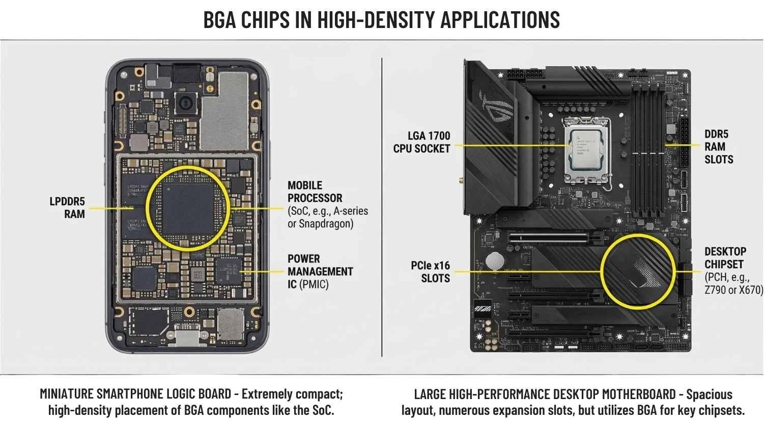
Figure: BGA chips mounted on a miniature smartphone logic board and a large, high-performance desktop computer motherboard.
BGA vs QFP vs LGA Packages
Selecting the appropriate integrated circuit package is an important design decision that affects PCB layout complexity, electrical performance, thermal management, and manufacturing reliability.
Ball Grid Array (BGA), Quad Flat Package (QFP), and Land Grid Array (LGA) packages are commonly used in modern electronics, each offering different advantages depending on application requirements.
Comparison of BGA, QFP, and LGA Packages
Feature | BGA Package | QFP Package | LGA Package |
|---|---|---|---|
Connection Method | An array of solder balls under the package | Gull-wing metal leads around package edges | Flat metal contact lands |
Pin Density | Very high | Moderate | High |
Electrical Performance | Excellent (short signal paths, low inductance) | Moderate | Good |
Thermal Performance | Very good (heat dissipates through PCB planes) | Limited | Good with heat spreader or socket |
PCB Routing Complexity | High (HDI techniques are often required) | Low | Moderate |
Inspection Method | X-ray inspection required | Visual inspection possible | Visual or AOI inspection |
Assembly Difficulty | High (automated placement and reflow needed) | Relatively easy | Moderate |
Typical Applications | CPUs, GPUs, FPGAs, high-speed ICs | Analog ICs, microcontrollers, interface chips | Desktop processors, RF devices |
Cost | Medium to high | Low | Medium |
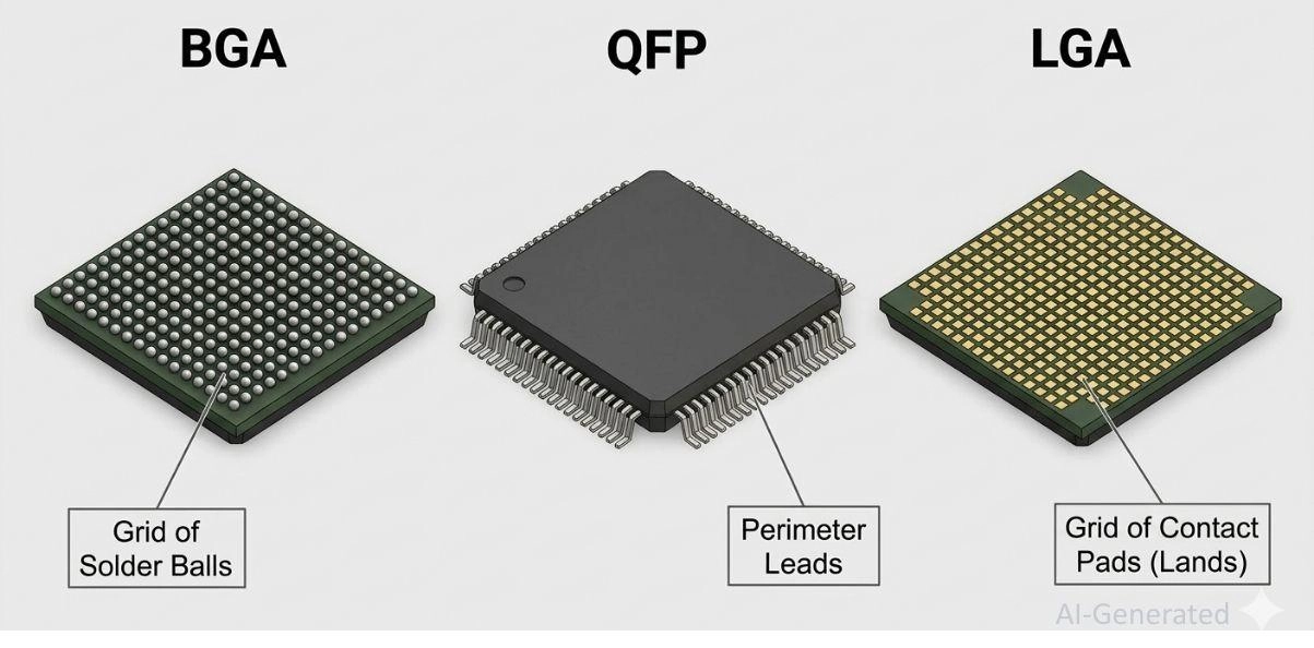
Figure: Comparing the physical connection methods of BGA (solder balls), QFP (metal leads), and LGA (flat contact pads) integrated circuits.
Design Considerations
- BGA packages are preferred in high-performance and high-density PCB designs because they provide superior signal integrity and efficient thermal dissipation. However, they require advanced PCB fabrication techniques and precise assembly processes.
- QFP packages are easier to route and inspect, making them suitable for simpler or cost-sensitive designs, although their leaded structure limits pin count and high-frequency performance.
- LGA packages offer a balance between density and accessibility. They are often used in socketed processor designs or RF modules, where mechanical clamping or controlled soldering ensures reliable electrical contact.
PCB Layout and Pad Design for BGA Chips
To ensure reliability, the PCB layout must be meticulously designed to accommodate the BGA chip.
SMD vs. NSMD Pads for BGA Chip
When laying out your board, you must choose between Solder Mask Defined (SMD) pads and Non-Solder Mask Defined (NSMD) pads. NSMD pads are generally preferred for BGA chips. In an NSMD layout, the solder mask opening is slightly larger than the copper pad. This allows the molten solder ball to grip not just the top of the copper pad, but also its sides, creating a much stronger mechanical bond that better resists thermal stress.
Escape Routing and Fan-out Techniques in BGA Pad
To get signals out from the inner rows of the BGA, engineers use "escape routing." For larger-pitch BGAs (0.8mm and above), "dog-bone" fan-outs are used, in which a short trace connects the BGA pad to an adjacent via. For ultra-fine-pitch BGAs, HDI techniques such as Via-in-Pad Plated Over (VIPPO) are required, in which the via is drilled directly inside the BGA pad, plated, and filled flat to save space. Careful solder pad design is critical here to prevent solder from wicking into empty vias, which can cause weak joints.
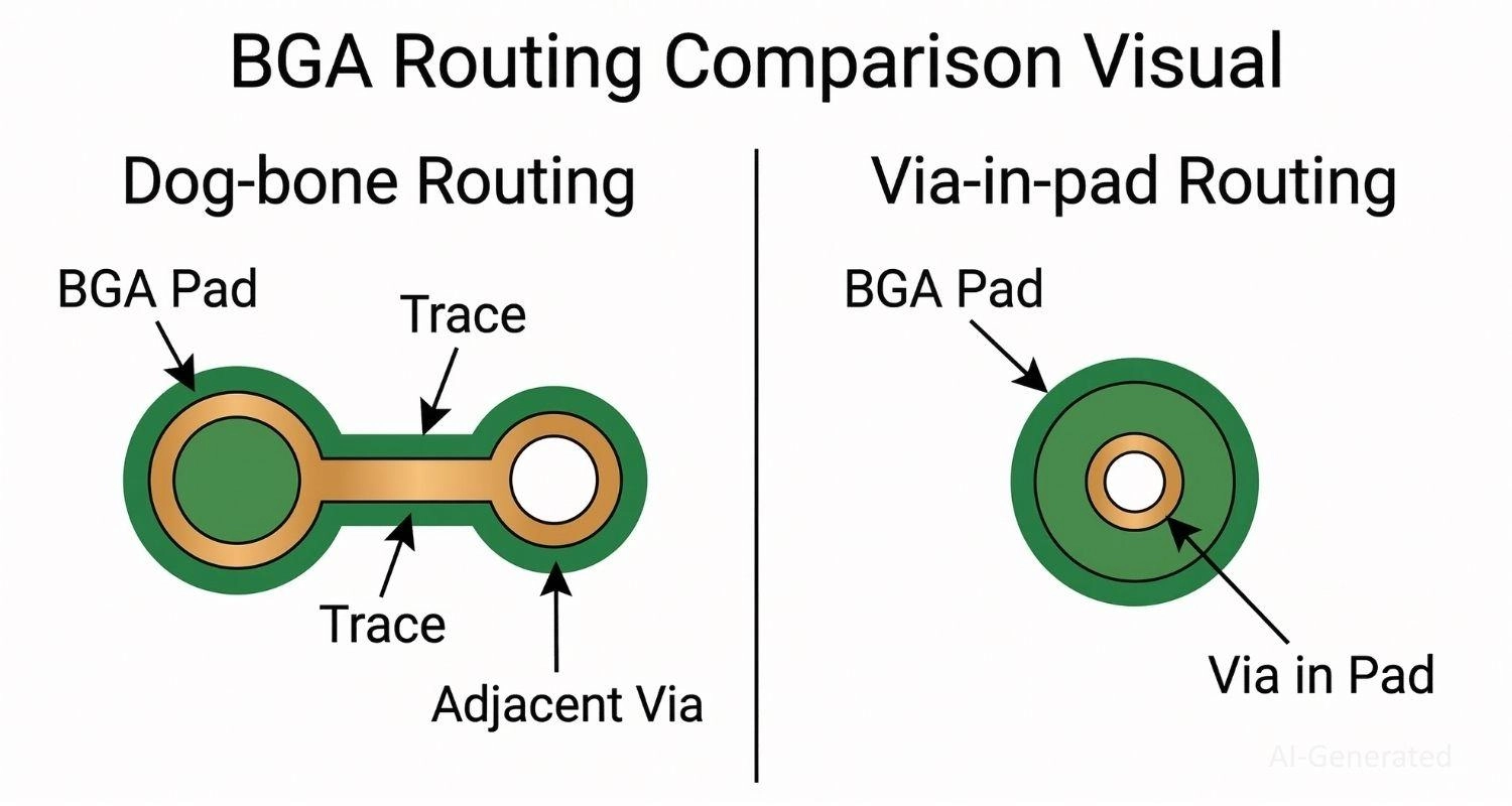
Figure: Showing dog-bone routing and via-in-pad escape routing techniques for BGA chips.
BGA Chip Assembly and Inspection
Assembling a BGA chip onto a printed circuit board requires high-precision automated manufacturing processes to ensure reliable solder joint formation. Unlike leaded packages, BGA solder connections are located beneath the component body and cannot be visually inspected after assembly.
Solder Paste Printing and Component Placement
The assembly process begins with accurate solder paste deposition using a metal stencil. Proper stencil thickness and aperture design are critical to achieving consistent solder volume. The BGA component is then placed on the PCB using automated pick-and-place equipment with optical alignment systems.
Reflow Soldering Process
During reflow soldering, the board passes through a controlled thermal profile consisting of preheating, soaking, peak reflow, and cooling stages. As the solder balls melt, surface tension helps self-align the BGA package with the PCB pads, forming reliable electrical and mechanical joints.
X-Ray Inspection of BGA Joints
Because the solder joints are hidden beneath the package, Automated X-Ray Inspection (AXI) is commonly used to verify joint quality. X-ray imaging can detect defects such as voiding, bridging, insufficient solder, and open connections that may affect long-term reliability.
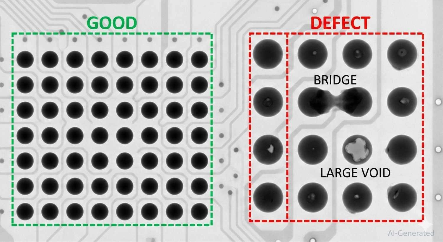
Figure: Comparison of X-ray image of BGA solder joints highlighting good joints, voiding, and bridging defects.
Reliable BGA PCB Assembly with JLCPCB
Designing with a BGA chip unlocks incredible performance, but handling the intricacies of HDI routing, strict reflow profiling, and X-ray inspection can be daunting. Partnering with an advanced manufacturer eliminates these bottlenecks.
Engineers can source genuine, moisture-controlled BGA chips directly through the JLCPCB Parts library, ensuring components are factory-fresh and ready for reflow. Once your layout is complete, JLCPCB's PCB Assembly services utilize state-of-the-art automated pick-and-place machines, precision multi-zone reflow ovens, and mandatory AXI (X-ray) inspection to guarantee every hidden solder joint is structurally sound.
Don't let BGA assembly limitations hold back your next high-density design. Get an instant quotation and transition smoothly from prototype to production with JLCPCB.
FAQs
Q: What is the main difference between a BGA and an LGA chip?
A BGA (Ball Grid Array) comes with pre-attached solder balls on its underside for direct reflow soldering. An LGA (Land Grid Array) features flat, gold-plated metallic contact pads. LGA chips are either clamped into a mechanical motherboard socket (like many modern desktop CPUs) or soldered down using printed solder paste.
Q: Can I solder a BGA chip by hand?
While highly experienced technicians can use a hot air rework station and flux to solder simple, low-pin-count BGA chips, it is strongly discouraged for reliable production. Precise optical alignment and exact temperature profiling are required to ensure the hidden joints form correctly, making automated assembly essential.
Q: What causes "voiding" in BGA solder joints?
Voiding occurs when flux gases, impurities, or moisture are trapped within the molten solder ball during reflow, forming internal air pockets. Excessive voiding weakens the joint's structural integrity and reduces its thermal and electrical conductivity.
Q: What is BGA reballing?
Reballing is a rework process used to salvage an expensive or hard-to-find BGA chip. It involves cleaning the old, oxidized solder off the chip's pads, placing a specialized micro-stencil over the bottom of the chip, applying fresh flux and loose solder spheres, and heating it so the new balls attach perfectly to the package.
Q: Why is X-ray inspection mandatory for BGA chips?
Because the solder joints are situated entirely beneath the opaque chip package, standard visual inspections and optical cameras cannot see them. X-ray imaging provides a non-destructive way to look "through" the silicon and substrate to verify joint integrity, ensuring there are no hidden shorts or open connections.
Conclusion
The BGA chip is a marvel of modern electronics packaging, serving as the foundational enabler for the miniaturization and explosive power of today's technology. By utilizing the entire chip footprint for I/O connections, BGAs address the physical limitations of perimeter-leaded packages while also offering superior thermal dissipation and electrical performance.
While they do introduce complexities in HDI layout and require advanced automated assembly and X-ray inspection, these hurdles are easily overcome by partnering with equipped manufacturing professionals. Understanding these guidelines ensures your next high-density BGA design will be robust, reliable, and ready to perform
Popular Articles
• SMD Capacitor Sizes: Complete Size Chart and Selection Tips for PCB Design and Assembly
• SMD Diode Code Lookup: Full List, Marking Guide & Identification [2026 Guide]
• SMD Resistor Package Sizes: Complete Size Chart, Footprints & How to Choose
• SMD Capacitor Codes: Identification, Markings, and Polarity
• How to Solder SMD Components Like a Pro [2026 Updated]
Keep Learning
SMD Transistor Code Lookup: Identify Markings, Pinout & Multimeter Test Guide
Repairing a circuit board often brings a familiar frustration: staring at a tiny, three-legged black component with an obscure two- or three-letter code. Whether troubleshooting a bare prototype or a mass-produced PCBA, knowing how to quickly decode these surface-mount device (SMD) markings is an essential skill for any electronics engineer or repair technician. In this comprehensive guide, you will learn: 1. How to decode SMD transistor marking codes 2. How to identify BJT vs MOSFET types 3. How to f......
SMD Capacitor Sizes: Complete Size Chart and Selection Tips for PCB Design and Assembly
In the world of modern electronics, surface mount devices (SMDs) have revolutionized board design, allowing for smaller, faster, and more efficient printed circuit boards. When designing a PCB, selecting the correct SMD capacitor sizes is one of the most critical decisions an engineer must make to ensure both electrical reliability and manufacturability. In this article, you will find practical, authoritative guidance on: Comprehensive SMD capacitor size charts for quick reference. How to read imperia......
SMD Diode Code Lookup: Full List, Marking Guide & Identification [2026 Guide]
In modern electronics, surface-mount diodes are used everywhere - from power input protection circuits to high-speed signal routing. Because these components are extremely small, manufacturers cannot print full part numbers on their bodies. Instead, they use short marking codes such as A2, M7, SS14, or SL, which often confuse beginners during PCB repair, reverse engineering, or component replacement. This guide explains how to decode SMD diode codes, identify polarity, test components using a multimet......
Thin Film vs. Thick Film Resistors: Key Differences & Selection Guide
Key Takeaways Default to thick film resistors for most designs. They are cost-effective, robust, and ideal for pull-ups, LED current-limiting, digital circuits, and surge-prone applications. Choose thin-film resistors whenever a resistor defines an analog quantity, such as a voltage divider, reference network, gain-setting circuit, or current-sensing signal chain. Their tight tolerance and low TCR help maintain measurement accuracy over temperature and time. Most PCB designs use thick film or thin fil......
Capacitor Types Explained: Applications, Differences, and Selection Guide
Capacitors are the most widely used parts in electronics design, from input/output coupling to bypassing and decoupling networks; they find applications everywhere. And if you get the wrong part/value placed, the consequences may be you get an audible whine from a supply rail, a bootloader that won't start, or a capacitor that lights up like a match. The question that never comes up is "which brand?" It's always “which type and what value.” This tutorial does not waste time on a textbook explanation o......
PoP Package (Package on Package) Explained: Architecture, Assembly, and SMT Challenges
In the race for miniaturization, fitting more processing power into smaller footprints is the ultimate challenge for PCB designers. Package on Package (PoP) technology answers this by integrating logic and memory vertically, becoming the standard for modern mobile processors. However, this 3D architecture demands advanced SMT assembly capabilities beyond standard fabrication. JLCPCB specializes in the high-precision manufacturing required to master these complex stacks. This guide covers how PoP packa......