Smart PCB Array Design for Higher Yield and Lower Production Costs
14 min
- Why PCB Array Design Matters in Modern Manufacturing
- Key Benefits of Well-Designed PCB Arrays
- Best Practices for Creating Effective PCB Arrays
- Manufacturing Considerations for High-Yield PCB Arrays
- JLCPCB's Strength in Efficient PCB Array Production
- FAQ about PCB Array
- conclusion
Key Takeaways
Smart PCB array design is a critical strategy for achieving higher manufacturing yield and significantly lower production costs. By optimizing panelization with proper board spacing, V-scoring, tab routing, and mouse bites, designers can dramatically improve material utilization by 20-30%, enhance production throughput, and simplify handling and depaneling while minimizing mechanical stress and defects. Effective use of fiducials and careful component clearance further ensures high-quality results, making well-designed PCB arrays essential for efficient volume production.
Ever wonder why, when you go from the prototype stage to volume production, the cost of your per-unit PCB falls through the roof? One decision that plays a big part in cost savings is how you lay out your boards on a manufacturing panel. It is known as PCB array design and is the key to a profitable production run versus a bleeding production run due to wasted materials and failed separations.
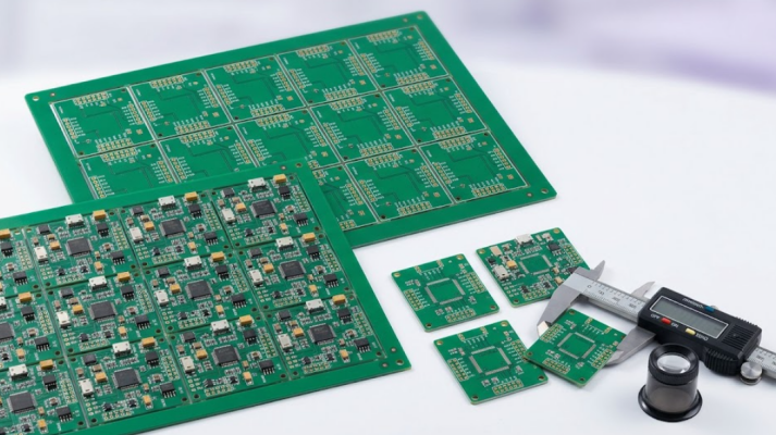
From a few small sensor modules to thousands of LED driver boards, how your individual PCBs are arranged on a production panel directly affects throughput, yield, and unit cost. A poor design wastes laminate, creates handling problems when putting the array together, and can even damage the laminate mechanically when depaneling. In this lesson, we will go over all the basics of designing a PCB array. Starting with the basics of what a PCB array is, to spacing, scoring, and tab routing best practices.
Why PCB Array Design Matters in Modern Manufacturing
What a PCB Array Is and Its Role in Panelization
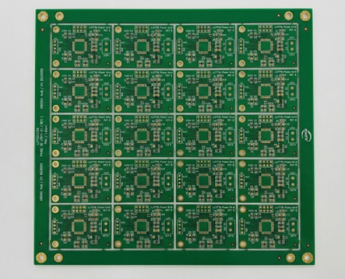
A PCB array, also known as a PCB panel or sub-panel, is a collection of identical (or sometimes different) individual PCBs that are arranged in a grid on a single manufacturing panel. Manufacturers treat the entire array as a single board and go through the entire manufacturing process of etching, drilling, solder paste printing, and reflow.
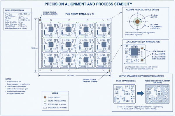
Most fabricators use 18 x 24” (457 x 610 mm) and 21 x 24” (533 x 610 mm) standard manufacturing panel sizes. These panels have a usable area in which your individual PCB designs are tiled and then a tooling strip (also known as a rail or border) that contains fiducial marks, tooling holes, and other alignment features.
Imagine cutting out cookies from a cookie sheet. The task is to put as many cookies as possible on each sheet of paper, but leave enough space between them so they can be easily cut. Your copper-clad laminate is the “dough,” and any leftover bits are wasted product and money.
Impact on Production Efficiency and Material Utilization
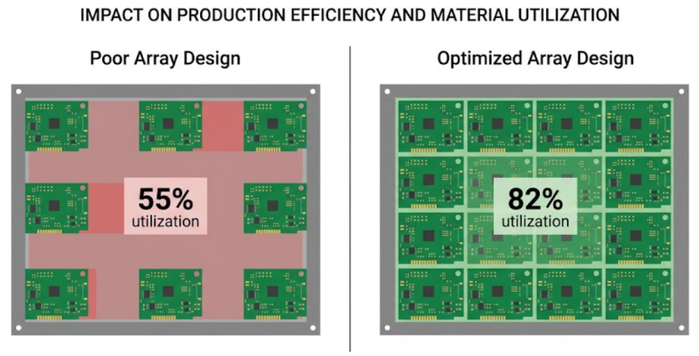
Your PCB array layout is directly related to cost and efficiency. With a well-optimized array, it is possible to get 20-30% more boards per panel than with a naive layout. Multiply that improvement by hundreds or thousands of panels, and the material savings alone can be huge.
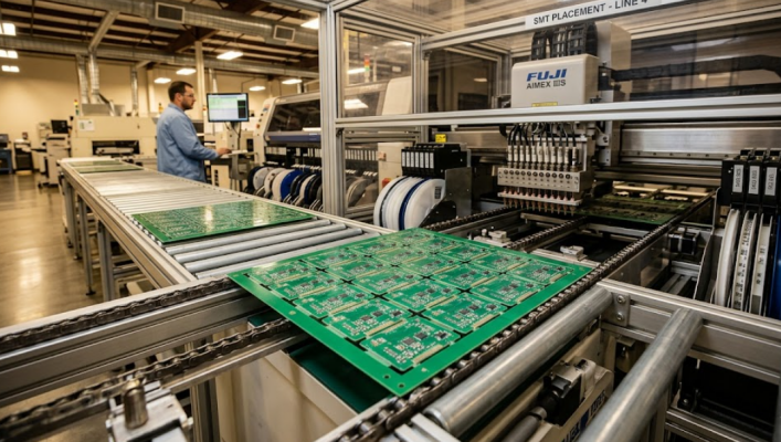
In addition to material utilization, array design has an influence on all subsequent processes. The pick and place machine can process the whole panel in one go during SMT assembly, and more boards per panel means higher throughput per machine hour. In the wave soldering or selective soldering process, the panel is moved through the machine as a whole. AOI inspection will take place on the camera, and one panel will be scanned, not individual boards.
Here is a quick look at how array optimization affects key production metrics:
| Metric | Poor Array Design | Optimized Array Design |
|---|---|---|
| Boards per panel | 8 | 12 |
| Panel utilization | 55% | 82% |
| Material waste | 45% | 18% |
| SMT cycle time per board | Baseline | ~33% reduction |
| Unit cost impact | Higher | Lower |
Key Benefits of Well-Designed PCB Arrays
Increased Throughput and Reduced Waste
The first advantage of a well-designed PCB array is increased throughput. The more boards you pack on each panel, the more boards each machine in the production line is processing per cycle. The stencil printer allows more boards to be printed per stencil. The pick and place machine places more boards per load of the panel. More boards can be cured in a single pass with the reflow oven.
This is particularly important for small PCBs as it allows for the increase of throughput gain. For instance, a small Bluetooth module measuring just 10 x 15 mm could accommodate more than 100 in a single manufacturing panel. If those small boards were not panelized, it would be difficult, if not impossible, to handle and assemble them individually. The array enables automation of assembly.
Some of the main advantages of key throughput are:
- Faster machine setup per unit (amortized over all boards in the array)
- Increases solder paste printing speed (one print covers the whole panel)
- Simultaneous placement and inspection of all boards in parallel.
- Reduce handling defects in relation to the processing of individual small boards
Improved Handling and Depaneling Ease
Handling of individual small PCBs can be a nightmare. They will block conveyor systems, slide through equipment, and are susceptible to edge damage. Panelization overcomes this by providing you with a larger standardized form factor that can easily pass through automated equipment.
However, the design of the array also affects the ease of separation of the boards at the end of the line. If not designed well, a depaneling operation can result in fractured solder joints, stressed components around the edges of the board, or rough/uneven edges on the board that can affect enclosure assembly. The spacing, separation, and location of breakaway features must be carefully considered at the outset. As a general guideline, components should be kept a minimum of 1.5mm from any V-scores and 2.0mm from any routed tab edges. This clearance helps to avoid mechanical stress upon separation that would otherwise occur at the sensitive solder joints.
Best Practices for Creating Effective PCB Arrays
Optimal Spacing, Orientation, and Panel Size Selection
You need to make three key decisions to get your array layout right: spacing between boards, the orientation of the boards, ds, and the targeted size of the panels.
The spacing between boards will vary based on how you are separating them:
- V-scoring: Minimum V0.0 mm between boards required as the scoring line is across the entire panel. There should be a gap, however, of 0.4-0.5 mm between the copper features and the board edge.
- Tab routing with mouse bites: Needs 1.6-3.0 mm space between boards, for the routed channel and breakaway tabs.
- Full routing with breakaway tabs: Needs 2.0 – 3.0 mm spacing for the routing bit (usually a 1.6 mm or 2.0 mm diameter end mill).
You might be surprised by the difference orientation can make. For rectangular or irregularly shaped boards, occasionally it is possible to turn the boards 90 degrees or mirror alternate rows to substantially boost the count/board. Always make several orientations and compare the results. Here is a general guideline for common panel sizes:
| Panel Size (mm) | Usable Area (mm) | Best For |
|---|---|---|
| 100 x 100 | 80 x 80 | Small prototyping batches |
| 150 x 150 | 130 x 130 | Medium-size boards |
| 200 x 250 | 180 x 230 | Production runs |
| 250 x 350 | 230 x 330 | High-volume small boards |
| 300 x 400 | 280 x 380 | Maximum efficiency |
Using V-Scoring, Tab Routing, and Mouse Bites Effectively
V-Scoring is the process of making a V-shaped cut at the top and bottom surfaces of the panel along the separation line. The thickness of the board is reduced by approximately one-third on each side by the groove, and the thin web of material snaps cleanly when bent. V-scoring is best applied to straight-edged rectangular boards, as the score line needs to extend across the width or length of the panel.
Key V-scoring specifications:
- Score angle: 30, 45, or 60 degrees (30 degrees is the most popular).
- Remaining web thickness: Usually 0.3-0.5 mm for a 1.6 mm board.
- Board-to-board gap: virtually none (the score line is the gap)
- Only works for straight lines that are extended across the entire panel length.
Tab routing is the process of cutting around the perimeter of each board in a panel, leaving small tabs (usually 3-5) on each board that keep the boards in the panel. The tabs are snapped or cut during de-paneling.
A refinement of tab routing is called a mouse bite (also known as a perforated tab or breakaway tab). The router leaves small tabs with a series of non-plated holes (usually 0.5-0.6 mm diameter, spaced 0.7-0.8 mm apart) drilled along the connection point, in place of the solid tabs. These perforations form a planned weak point that breaks easily without the need for excessive force.
The following comparison will help you decide:
| Feature | V-Scoring | Tab Routing | Mouse Bites |
|---|---|---|---|
| Board shape | Rectangular only | Any shape | Any shape |
| Edge quality | Very smooth | Moderate (tab nubs) | Good (slight nubs) |
| Mechanical stress | Low | Moderate | Low-moderate |
| Component clearance | 1.5 mm from the score | 2.0 mm from edge | 2.0 mm from edge |
| Best for | Simple rectangular boards | Irregular shapes | Irregular shapes, sensitive components |
| Tooling cost | Low | Moderate | Moderate |
Manufacturing Considerations for High-Yield PCB Arrays
Precision Alignment and Process Stability
To achieve high-yield array production, precise registration throughout the panel is required. With dozens of boards per panel, any registration issues with layers, solder mask, or silkscreen are compounded with each board. The 0.1mm registration error may be acceptable on a single board, but on a panel of 50 units, it could be enough to move edge-case designs out of spec.
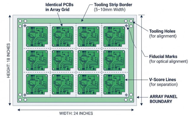
Fiducial marks are the key to your alignment. Placing fiducials on the tooling strip (global fiducials) and on or near individual boards (local fiducials) creates a global alignment for the whole panel and fine-tuning for each individual board. Local fiducials on each individual board in the array are highly recommended for arrays with fine-pitch components (0.5 mm pitch or less).
Fiducial placement is done as follows:
- Set up at least two global fiducials on the diagonal corners of the panel tooling strip.
- If required by your assembly house, add a 3rd global fiducial for rotational correction.
- Near fine pitch components: Use local fiducials (QFP, BGA, QFN packages).
- Fiducial diameter: 1.0-1.5 mm, clearance area is 2.0-3.0 mm without copper and solder mask.
- Avoid positioning fiducials near the edge of the panel where they can be hidden by clamping.
Quality Control During and After Panelization
Arrayed panels have two levels of quality control: panel and individual board. Both are of importance to sustain high yield.
Manufacturers certify at the panel level:
- Size and straightness of panels as a whole
- Accuracies in tooling hole position (usually within ± 0.05 mm)
- V-score depth consistency for the entire length of the panel
- Tab positioning and mouse bite hole positioning
- Panel warpage (IPC-A-600 calls up to 0.75% bow and twist in surface mount board)
Standard quality checks are in place at the individual board level:
- Continuity and isolation testing (flying probe or bed of nails)
- AOI for solder joint quality (after assembly)
- Impedance Check for controlled impedance design
- Radiographic inspection (X-ray) of BGA and/or hidden joints (if applicable).
However, one factor that is often overlooked is depaneling damage. The requirements of IPC-A-610 Class 2 state that the separated edge of the board should not contain any cracks, delamination, or exposed copper that would hinder reliability. Upon post-depaneling inspection, the clean separation shall be verified with no fractures that extend into the functional area of the board.
JLCPCB's Strength in Efficient PCB Array Production
Expert Panel Layout Optimization for Maximum Material Utilization
If you're considering setting up a PCB array, a deep understanding of panelization by your manufacturing partner can be a game-changer. JLCPCB's engineering team will process all the array submissions and conduct a review to ensure the best utilization of materials, while the ordering system on their website will offer instant feedback on the panel configuration.
They provide standard and custom panel sizes, so you can select the panel that will fit the most boards. If you prefer to work on your own panelization, JLCPCB supports pre-panelized Gerber files. If you prefer to let the professionals do the work, they can design an optimized array layout for your specific board design, which they are likely to fit more units into than a manual layout.
Seamless Support from Array Design Review to Final Delivery
The practical benefits of using JLCPCB include the seamless process from design to delivery. Their system automatically checks your Gerber files for potential panelization problems such as insufficient edge clearance for V-scoring, positioning tabs too near components, copper features that enter routing channels, and more.
In the event of problems, their engineering team offers constructive comments instead of simply saying no. The collaborative process results in fewer revision cycles and a quicker time to production. With their 1-2 day turnaround on PCBs and the competitive pricing that starts at $2, the cost of getting a good panelized design into production is quite low.
FAQ about PCB Array
Q: What is a PCB array?
A PCB array is a layout in which multiple identical PCBs are arranged in a grid pattern on a single manufacturing panel. This arrangement allows all boards to be fabricated and assembled simultaneously, improving production efficiency and reducing per-unit cost.
Q: How many boards can I fit in a PCB array?
The number depends on your individual board dimensions, the panel size, board-to-board spacing, and the tooling strip width. A PCB array calculator can help you determine the optimal count. For example, a 20 x 30 mm board on a 200 x 250 mm panel might fit 40 or more units with proper optimization.
Q: What is the difference between V-scoring and mouse bites?
V-scoring cuts a V-shaped groove across the full panel for straight-line separation. Mouse bites use a series of small drilled holes along breakaway tabs, allowing separation of irregularly shaped boards. V-scoring gives smoother edges, while mouse bites offer more design flexibility.
Q:How much spacing should I leave between boards in an array?
For V-scoring, you can use essentially zero spacing (the score line is the boundary), but keep copper features at least 0.4-0.5 mm from the board edge. For tab routing and mouse bites, leave 1.6-3.0 mm between boards to accommodate the routing channel.
conclusion
Mastering smart PCB array design is one of the most effective ways to transition smoothly from prototyping to high-volume production. A well-optimized panel layout not only maximizes material utilization and boosts manufacturing yield by 20-30%, but also improves throughput, reduces handling defects, and lowers overall production costs. By applying the right panelization techniques — whether V-scoring for rectangular boards or mouse bites and tab routing for complex designs — along with proper fiducial placement and component clearance, you can achieve cleaner edges, higher reliability, and smoother assembly.
Ultimately, thoughtful array design turns your PCB panel into a competitive advantage. Partner with an experienced manufacturer like JLCPCB to refine your panelization strategy and bring your boards to market faster and more profitably. Start optimizing your next production run today.
Keep Learning
Understanding SMT PCB Boards Technology: An Essential Component of Modern Electronics
Surface Mount Technology (SMT) has changed manufacturing of modern electronics. It has made designs and assembly methods more efficient. Many modern electronics depend on SMT PCB boards, which make it possible for circuit designs to be small and efficient. This is what today's technology needs. This article discuss about many types of SMT PCB boards, their uses, and the best methods for designing and assembling them. 1. What is an SMT PCB Board? Printed circuit boards called SMT PCB boards, use surfac......
How to Choose the Right Prepreg Material for Reliable Multilayer PCB
Have you ever wondered what makes all those copper layers stick to a cross-section of a multilayer PCB? Prepreg material is the answer, and it is of much more importance than most engineers think it is. Choose the prepreg selection wrong, and you are predetermined to delamination, impedance drift, and long-term reliability problems. Prepreg is not only glue. It is a designed composite that determines your dielectric separation, dictates your impedance, affects signal loss, and determines your board be......
Via Filling Explained: Key Techniques, Benefits, and Solutions for High-Performance PCBs
Key Takeaways Via filling completely fills plated through-holes and microvias with epoxy or conductive copper paste, followed by planarization and copper capping (POFV). It eliminates voids, solder wicking, and thermal/mechanical issues while enabling reliable via-in-pad designs. Benefits include superior heat dissipation (up to 8 W/m·K), better signal integrity, higher mechanical strength, and improved assembly yields. JLCPCB provides free non-conductive filling + POFV on 6+ layer boards. Ideal for H......
How Fiducial Markers Guarantee Perfect Alignment in Professional PCB Fabrication
Today, the most sophisticated pick-and-place machine can place a 0.5 mm pitch QFP on its footprint, board after board, thousands of times, and never miss. It is not only a matter of expensive cameras or high-quality servos, but it begins with a little, very small copper dot, simply hanging there in the corner of your PCB. That dot represents a fiducial marker, and without it, even the smoothest SMT line would be laying components in the dark. The unrecognized heroes of automated assembly are the fiduc......
Technical Guidance: Character Design Specifications
To facilitate component assembly, future maintenance, and traceability of PCB manufacturing information (such as manufacturer, production date, batch number, etc.), various character markings are typically silk-screened onto the PCB. These include component designators, polarity marks, test point labels, company logos, and production traceability information. Traditional PCB character silk-screening uses the screen printing process, hence the term “silk-screen characters.” High-definition characters a......
Step-by-Step Guide to the Printed Circuit Board Manufacturing Process
Key Takeaways Core Role: PCBs provide the physical foundation and electrical connections for modern electronics. Multi-Step Process: Manufacturing spans design imaging, substrate creation, inner/outer layer etching, lamination, and surface finishing. Precision & Quality Control: Features micro-drilling (down to 100 µm) for layer connectivity, Automated Optical Inspection (AOI), and final electrical testing. Protection & Finish: Solder masks and surface finishes (e.g., ENIG, HASL) protect copper traces......