
Border Layer Thickness: Impact on PCB Dimensions and V-Grooves
7 min
- Example Scenario
- Handling Shapes and Grooves
- Why Centerline Referencing Ensures Manufacturing Consistency
- FAQ about Border Layer Thickness
- Conclusion
Key Takeaways
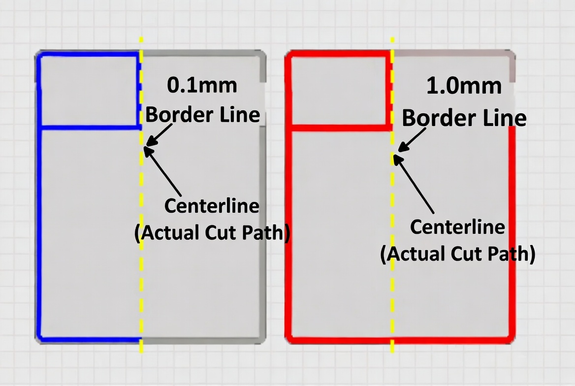
The line width of the Border Layer has no impact on final PCB dimensions or V-groove (V-cut) characteristics. At JLCPCB, all routing and scoring operations reference the centerline of the Mechanical Layer outline, ensuring consistent board size with ±0.1mm precision and uniform 25° V-cuts regardless of whether you use 0.1mm or 1.0mm lines. Understanding this centerline principle allows designers to focus on visibility and clarity in EDA tools while achieving reliable, high-precision manufacturing results every time.
When it comes to designing a PCB, understanding the implications of border layer (board outline) thickness is essential for accurate fabrication and panelization. In this blog post, we will examine a practical example with different line widths on the Border Layer (0.1mm vs 1.0mm) to clarify their effects on final board dimensions and V-cut (V-groove) processing during panelization. We will also cover key JLCPCB manufacturing considerations to help you avoid common DFM issues.
Example Scenario
Imagine we have a PCB design with two different line widths on the border layer: 0.1mm and 1.0mm, respectively. Now let's address the following questions:
Will the dimensions of the final board be different?
No. The thickness (line width) of the border lines does not directly impact the overall dimensions of the board. At JLCPCB, all routing and cutting operations reference the centerline of the border lines defined on the Mechanical Layer (typically Mechanical 1/GM1). Whether your border line is 0.1mm or 1.0mm wide, the final board outline remains consistent.
Typical Dimension Tolerances at JLCPCB:
· CNC Routing: ±0.1mm (Precision) / ±0.2mm (Regular)
· V-scoring: ±0.4mm (slightly larger due to material expansion during separation)
This centerline-based approach ensures high precision and repeatability across different design tools.
During panelization, will the V-grooves be cut according to the thickness of the border layer?
No. V-grooves (V-cuts) are processed according to JLCPCB’s predefined specifications and are completely independent of the border line width. The V-cut is performed along the centerline with a standard 25° angle, typically leaving about 1/3 of the board thickness as connecting material for easy manual or roller separation.
Key JLCPCB V-Cut Specifications:
| Parameter | Specification | Notes |
|---|---|---|
| V-Cut Angle | 25 degrees | Double-sided V-cut |
| Min Panel Size | 70mm x 70mm | Both length and width |
| Min Connecting Edge | 3mm (≥5mm for ≤0.8mm thick) | Rectangular boards |
| Copper Clearance to Centerline | ≥0.4mm | To prevent copper exposure |
| Not Supported | 0.4mm board thickness | - |
| Dimension Tolerance | ±0.4mm | Due to separation |
V-cuts must be straight horizontal or vertical lines that span the entire panel. This standardization guarantees uniform groove depth and strength regardless of your design’s border line width.
Handling Shapes and Grooves
To gain a comprehensive understanding, let's also discuss how shapes and grooves are handled in such a scenario.
Shapes drawn inside the board:
When designing shapes within the board, such as cutouts or internal features, they are typically routed based on the centerline of the line. The actual width of the shape will be determined by the routing tool, irrespective of the border line's width.
Why Centerline Referencing Ensures Manufacturing Consistency
Beyond the direct impact on dimensions and V-grooves, understanding the centerline referencing principle is crucial for achieving consistent results across different PCB designs and panelization methods. At JLCPCB, the fabrication system interprets all Mechanical Layer border lines by their geometric center. This means that even if you intentionally draw a very thick 1.0mm border line for better visibility in your EDA software, the actual CNC routing tool or V-scoring blade will always follow the exact center path.
approach offers several key advantages
- Dimensional Stability: Final board size remains identical regardless of line width, with standard CNC routing tolerance controlled within ±0.1mm (precision) to ±0.2mm (regular).
- V-Cut Reliability: The 25° V-scoring process maintains uniform remaining thickness (approximately 1/3 of total board thickness), ensuring boards separate cleanly without cracking or leaving excessive material.
- Error Reduction: It eliminates ambiguity caused by varying design habits across KiCad, Altium, or Eagle, preventing common panelization issues such as misaligned grooves or oversized boards.
Practical Design Recommendations
When working with border layers, we recommend:
1. Set line width between 0.1mm and 0.5mm for optimal visibility without cluttering the view.
2. Always place the primary board outline on Mechanical Layer 1 (GM1), as it receives processing priority.
3. Maintain at least 0.4mm copper clearance from the centerline of any V-cut to avoid burrs or short circuits after separation.
4. For high-precision applications (e.g., RF or tight-tolerance mechanical assemblies), consider adding alignment marks near the border to further verify post-fabrication dimensions.
By following these centerline-based practices, engineers can confidently use different line widths during the design phase without worrying about downstream manufacturing variations. This standardized method is one of the reasons JLCPCB can deliver consistent quality even for complex multi-board panels.
Solid lines used to depict grooves:
For solid shapes, including filled polygons or copper pours, they are manufactured based on the actual width of the drawn shape. The thickness of the border layer does not influence the dimensions of internal solid shapes on the PCB.
FAQ about Border Layer Thickness
Q: Does changing the border layer line width affect the final PCB dimensions?
No. At JLCPCB, all cutting operations (CNC routing and V-scoring) are based on the centerline of the border lines on the Mechanical Layer. Whether your line width is 0.1mm or 1.0mm, the final board size remains exactly the same.
Q: Will different border line widths result in different V-groove (V-cut) depths or thicknesses?
No. V-cuts are processed according to JLCPCB’s standardized specifications (25° angle, ~1/3 board thickness remaining) and are completely independent of your border line width.
Q: Which Mechanical Layer should I use for the board outline?
We strongly recommend using Mechanical Layer 1 (GM1) for the primary board outline. This layer has processing priority and helps avoid manufacturing confusion.
Q: What is the recommended border line width for best results?
A line width between 0.1mm and 0.5mm is ideal. It provides good visibility in your design software without cluttering the layout. Thicker lines (e.g. 1.0mm) are fine for visibility but offer no manufacturing advantage.
Q: What is the copper clearance requirement near V-cuts?
Please keep copper at least 0.4mm away from the centerline of any V-cut. This prevents burrs, short circuits, or exposed copper after board separation.
Q: Can I mix different border line widths in the same design or panel?
Yes, you can. As long as the centerlines are consistent, JLCPCB’s manufacturing system will produce accurate and uniform results. Different widths are only for your design visibility and will not affect the final product.
Conclusion
In this example, we have explored the impact of different line widths on the border layer of a PCB design. We have learned that the thickness of the border line does not affect the board dimensions, as all cuts are referenced to the centerline of the border lines. Additionally, V-grooves are cut according to predefined specifications, independent of the border layer thickness.
Understanding these concepts is crucial for designing PCBs accurately. By considering the relationship between border layer thickness, board dimensions, and V-grooves, you can ensure the desired outcomes in your PCB fabrication process. JLCPCB hope this example has shed light on the topic. If you have any further questions or need assistance with your PCB design, feel free to reach out to us.
Keep Learning
Why Accurate NPTH Design Matters for Reliable PCB Manufacturing
Key Takeaways NPTH are mechanical holes (no copper plating) used for mounting, alignment, and tooling. Poor NPTH design often causes PCB cracks during assembly or screw tightening. Follow key rules: ±0.08 mm tolerance, ≥0.5 mm diameter, 0.2–0.3 mm copper clearance. Keep adequate material around edge holes and clearly mark NPTH in fabrication files. Proper NPTH design + DFM checks ensure reliability from prototype to mass production. Ever get a slight crack in a finished PCB when putting it into an enc......
How to Design and Manufacture Reliable Slot Holes in PCBs
Key Takeaways Slot holes are elongated openings ideal for flat pins, connectors, shields, and board alignment. Minimum sizes: 0.5 mm (plated) and 1.0 mm (non-plated); prefer rounded ends with length ≥ 2.5× width. Maintain proper annular ring, edge clearance, and DFM rules to prevent breakout and plating issues. Use overlapping drills for short plated slots and routing for longer ones. Good slot design greatly improves mechanical strength, thermal performance, and assembly reliability. JLCPCB’s precisi......
How Beveled Edges Improve Reliability and Performance in Card Edge Connectors
Key Takeaways Beveled edges enable smooth insertion and protect gold fingers from wear in card edge connectors. Use 30° or 45° angles (45° is standard for most designs) with depth of 1/3 to 1/2 board thickness. They reduce insertion force, prevent plating damage, and improve long-term contact reliability. Proper beveling is critical for high-cycle applications like DDR modules and PCIe cards. Bevel edges came into my attention the first time a memory module that I designed scratched its own gold finge......
How to Prepare Perfect Gerber Files for Flawless PCB Production
Key Takeaways Use RS-274X format and consistent millimeter units for all files. Always include complete layers: Copper, Solder Mask, Silkscreen, Board Outline, and NC Drill. Check your Gerbers in a viewer before uploading to catch errors early. Follow DFM rules: proper annular rings, solder mask expansion, and trace spacing. Use clear file naming and detailed fabrication notes. After spending weeks working on the perfect board layout, the routing is clean, the DRC passes, and you hit “export.” Two day......
Technical Guidance: V-Cut Panelization Standards
For boards with regular rectangular shapes, V-cut (V-scoring) panelization is an efficient method. This process involves cutting V-shaped grooves of a specific depth on both sides of the panel along the board boundaries, leaving a thin web of material (typically about 1/3 of the board thickness) that allows easy manual separation after SMT assembly. After separation, minor thread-like fibers or rough edges may remain and can be lightly scraped off. Due to material expansion and cracking during depanel......
Technical Guidance: Character Design Specifications
To facilitate component assembly, future maintenance, and traceability of PCB manufacturing information (such as manufacturer, production date, batch number, etc.), various character markings are typically silk-screened onto the PCB. These include component designators, polarity marks, test point labels, company logos, and production traceability information. Traditional PCB character silk-screening uses the screen printing process, hence the term “silk-screen characters.” High-definition characters a......