
Achieving Clean PCB Separation: The Benefits of Professional Depaneling
12 min
- Why Depaneling Is a Critical Step in PCB Production
- Main Depaneling Methods and Their Applications
- Choosing the Right Depaneling Method for Your Project
- Common Depaneling Challenges and Professional Solutions
- JLCPCB's Advanced Depaneling Capabilities
- FAQ about PCB Depanelization
Key Takeaways
Clean depaneling is a critical final step: a poor split can cause microcracks, trace/solder-joint damage, delamination, and rough edges. Choose the method early based on outline, material/thickness, component edge clearance, volume, and required edge quality—V-scoring for fast straight cuts, routing for complex shapes, and laser for fragile or edge-constrained designs—with IPC criteria guiding controls and inspection.
Have you ever broken a PCB off a panel and found rough edges, small cracks along the board outline, or even a hairline crack running through a trace along an edge? That is what occurs when depanelization is bad. It is the final big mechanical process in PCB manufacturing, but it is also one of the most neglected when engineers are designing their projects. In the production process, PCBs are assembled in small groups on a bigger panel to enhance ease of handling and to facilitate automated assembly. However, when soldering and inspection are done, those boards must be separated in a clean manner.
Any bad depaneling process may negate all the meticulous work done in the fabrication process, adding stress fractures, delamination, or cosmetic flaws. Today, we are going to discuss the principal PCB depaneling techniques, trade-offs, and pitfalls you should be aware of. Whether you are creating prototypes or ramping up to thousands of units, learning depaneling will enable you to make wiser choices regarding panel design and methodology choice.
Why Depaneling Is a Critical Step in PCB Production
One can imagine depaneling being as simple a process as tearing boards in two, but the truth of the matter is much more complex. Board reliability, edge quality, and long-term electrical performance directly depend on the method you use and how well it is done.
The Role of Depaneling After Panelization
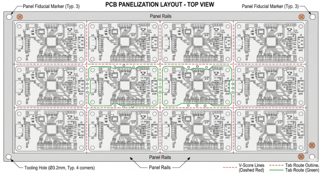
PCB manufacturing involves placing individual board designs onto a larger panel to be processed using automated SMT lines, reflow ovens, and wave soldering systems. This step of panelization is necessary in managing efficiency and cost reduction. After assembly, it is necessary to peel each board off the panel without causing any mechanical stress, thermal damage, or dimensional changes. The tolerances are very narrow, and the edge accuracy may be as small as 0.1 to 0.5 mm in some methods.
Risks of Poor Separation on Final Board Quality
The effects of poor depaneling may be instant or may manifest themselves months later in the field:
- Microcracks in the substrate: Overloading causes microscopic cracks in the laminate, reducing the structural strength of the board.
- Copper trace damage: Traces that are less than 0.3 mm from the board edge can be torn apart when rough separation occurs.
- Solder joint stress: BGA and QFN joints along the edge may crack due to flexural stress, resulting in intermittent connections.
- Delamination: Uncontrolled cutting forces may cause the copper-laminate interface to be separated all along the board perimeter.
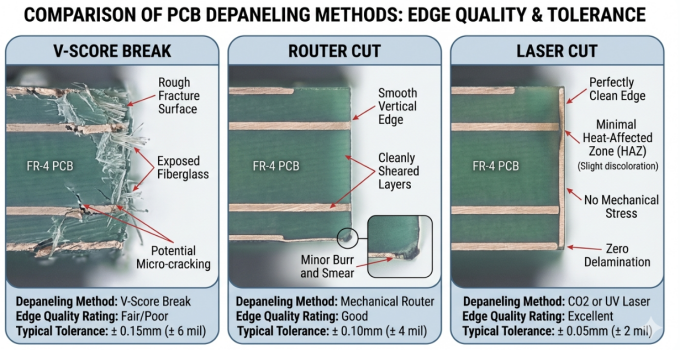
The IPC-A-600, Class 3 high-reliability boards require clean, smooth edges with no measurable delamination, burr, or fiber exposure exceeding specified limits.
Main Depaneling Methods and Their Applications
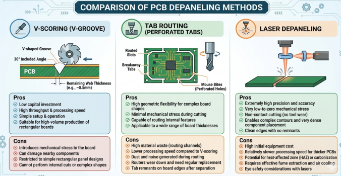
V-Scoring for Straight and Cost-Effective Separation
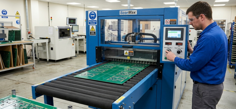
One of the oldest and least expensive PCB depaneling methods is V-scoring. In the process of fabrication, a V-shaped cut is made on the top and bottom surfaces of the panel along the separation lines. The groove usually cuts one-third of the thickness of the board on either side, and the slender web that remains to hold the panel together during assembly.
The boards are then separated by either taking the panel through a PCB depaneling machine that moves the panel through circular rotating blades or by exerting a controlled bending force. Key specifications include:
- Scoring angle: typically 30 degrees, 45 degrees, or 60 degrees
- Remaining web thickness: usually 0.2 to 0.5 mm (commonly one-third of total board thickness)
- Board thickness range: 0.8 mm to 3.0 mm
- Edge clearance for components: minimum 1.0 mm recommended from the V-score line
The main limitation is that V-scoring only supports straight cuts. Curves, irregular outlines, or internal cutouts require a different method.
Routing and Tab Routing for Complex Shapes
Tab routing is the preferred choice when board outlines contain curves or irregular shapes. The panel frame is attached to individual boards by small breakaway tabs (or mouse bites), usually 1.5 to 3.0 mm wide with non-plated holes to form a controlled weak point.
The high-speed carbide bit (20,000 to 60,000 RPM) is used in a PCB depaneling router to cut through these tabs with accuracy within 0.1 mm. The benefits of this are:
- Supports complex board shapes, including curves, notches, and internal cutouts
- Handles board thicknesses from 0.4 mm to over 3.0 mm
- Leaves relatively clean edges with minimal burring
- Compatible with rigid FR4, metal-core, and CEM substrates
The sacrifice is speed. Routing is not as fast as V-score separation, and small nubs left by breakaway tabs may need secondary finishing. Another factor is dust generation, where adequate extraction systems should be used around delicate parts.
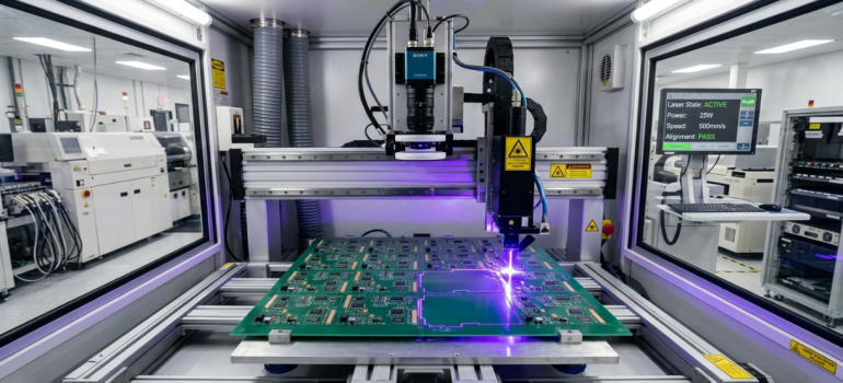
Laser Depaneling for High-Precision and Fragile Boards
Laser depaneling is the best option to ensure the utmost accuracy and a soft separation. The laser beam is focused on the PCB material and cuts without mechanical contact, providing a very clean edge with virtually no stress on the board.
Laser depaneling is particularly helpful in:
- Board boards that are ultra-thin (less than 0.4 mm) and are not able to resist mechanical routing forces.
- Flex and rigid-flex circuits in which the substrate is flexible and thus hard to clamp.
- Components are as close as 0.2 mm to the board edge.
- Medical or aerospace uses that need burr-free, carbonization-free edges.
UV lasers (usually with a wavelength of 355 nm) are desirable since they leave a smaller heat-affected zone (HAZ) compared to CO2 lasers. The kerf is very thin, as little as 20 to 50 micrometers, resulting in less material waste and a smaller nest of boards in the panel.
The main drawbacks are cost and throughput. Laser systems are very costly compared to mechanical ones, and are slower in cutting thicker boards. Routing or V-scoring is still more feasible with standard FR4 in moderate to high volumes.
Choosing the Right Depaneling Method for Your Project
Selecting the right method is not a one-size-fits-all decision. Making the wrong choice can mean paying more than necessary or compromising board quality.
Factors Like Board Thickness, Material, and Volume
The following table summarizes how the three methods compare across key selection criteria:
| Factor | V-Scoring | Tab Routing | Laser Depaneling |
|---|---|---|---|
| Board Shape | Straight lines only | Any shape, including curves | Any shape, including curves |
| Thickness Range | 0.8 - 3.0 mm | 0.4 - 3.0+ mm | 0.1 - 1.6 mm (typical) |
| Edge Accuracy | +/- 0.2 mm | +/- 0.1 mm | +/- 0.05 mm |
| Mechanical Stress | Moderate (bending force) | Low to moderate | Virtually zero |
| Component Edge Clearance | Min 1.0 mm | Min 0.5 mm | Min 0.2 mm |
| Material Compatibility | FR4, CEM-1 | FR4, MCPCB, CEM | FR4, Flex, Rigid-Flex |
| Tooling Cost | Low | Moderate | High |
| Best Volume Range | Medium to High | Low to High | Low to Medium |
Board material matters too. Standard FR4 works well with all three methods. Metal-core PCBs are better suited to routing due to the hardness of the metal layer. Flexible polyimide circuits almost always require laser depaneling to avoid tearing or distortion.
Balancing Speed, Cost, and Edge Quality
When volume is high and boards are simple rectangles, V-scoring is hard to beat on cost and speed. For prototype and low-volume runs with irregular shapes, tab routing provides the best balance of flexibility and cost. Laser depaneling makes economic sense when material fragility, extreme component-to-edge proximity, or strict edge requirements demand it.
Here is a practical decision framework:
Common Depaneling Challenges and Professional Solutions
Preventing Burrs, Cracks, and Mechanical Stress
Burrs are small raised ridges left on the board edge after cutting, most common when the router bit is worn, or the feed rate is too high. They are not just cosmetic. Burrs can interfere with enclosure fit, damage conformal coating integrity, or create short-circuit risks if conductive debris breaks loose.
Cracks and mechanical stress are more insidious. During V-score separation, if the remaining web is too thin, the board can break prematurely during handling. If it is too thick, excessive force radiates into the board as flexural stress. IPC-2221 recommends maintaining adequate clearance between the separation line and the nearest copper features to minimize stress-induced damage.
Professional solutions include:
- Using sharp, regularly maintained tooling with defined replacement intervals
- Optimizing V-score depth to balance panel rigidity with clean separation
- Applying controlled fixture support to distribute separation forces evenly
- Performing post-depaneling inspection per IPC-A-600 edge quality criteria
Ensuring Clean Edges Without Delamination
Delamination occurs when PCB laminate layers begin to separate along the board edge. This is especially problematic in multilayer boards, where exposed internal layers invite moisture ingress and can lead to conductive anodic filament (CAF) growth over time.
Preventing edge delamination requires attention across the process:
- Maintaining proper lamination quality, as weakly bonded laminates are more prone to separation
- Using the correct feed rate and RPM for routing to avoid excessive heat at the cut edge
- Keeping V-score angles and depths within specification to avoid stress concentration
- For laser depaneling, controlling power and speed to prevent resin damage
This is also why most production workflows depanel after assembly and reflow are complete. Depaneling before reflow leaves rough edges that high soldering temperatures can cause to propagate further.
JLCPCB's Advanced Depaneling Capabilities
Precision Equipment for Multiple Depaneling Techniques
Under a single roof, JLCPCB runs specific V-scoring lines, CNC routing stations, and laser depaneling lines. You have a design that requires straight-line V-score separation, or you have a complicated routed outline with breakaway tabs; the proper equipment can be found and held to tight tolerances. The routing systems are equipped with high-precision spindles that have automatic tool wear supervision to ensure the quality of edges. In the case of V-scoring, alignment of blades and depth of groove are checked during setup and during the batch.
Integrated Quality Control for Damage-Free Results
The depaneling process at JLCPCB is part of the overall quality control process. Separated boards are subjected to visual inspection and AOI to ensure edge integrity, dimensional accuracy, and no delamination or cracking. This is in line with IPC-A-600 Class 2 and Class 3 inspection requirements. In case a defect in depaneling is noted, the feedback loop to the fabrication and panelization teams will make sure the problem is solved at the origin, not the symptom.
Scalable Solutions from Prototype to High-Volume Runs
For prototype orders starting from just $2, you get the same depaneling precision applied to a 5-piece batch as you do to a 10,000-piece production run. The DFM review also helps you optimize tab placement and V-score lines, catching potential depaneling issues before fabrication begins. If you are looking to put these principles into practice, JLCPCB's integrated PCB fabrication and assembly services make it straightforward to go from design files to cleanly separated, fully assembled boards.
FAQ about PCB Depanelization
Q: What is depanelization in PCB manufacturing?
Depanelization is the process of separating individual PCBs from a larger production panel after assembly is complete. It is the final mechanical step that delivers individual boards ready for use or integration.
Q:What is the difference between V-scoring and tab routing?
V-scoring cuts a V-shaped groove along straight lines, and boards are snapped apart after assembly. Tab routing uses breakaway tabs and a CNC router to cut boards free. V-scoring is faster for rectangular boards, while tab routing handles complex shapes and curves.
Q: Can laser depaneling work on thick FR4 boards?
Laser depaneling is most effective on boards up to about 1.6 mm thick. For thicker boards, the cutting speed drops, and the heat-affected zone increases. Routing or V-scoring is more practical above 1.6 mm.
Q: Does depaneling affect solder joint reliability?
It can if done improperly. Excessive stress during separation can transmit flexural forces to nearby solder joints. BGA and QFN packages are the most vulnerable. Proper fixturing and adequate edge clearance minimize this risk.
Q: What IPC standards govern depaneling quality?
IPC-A-600 defines acceptability criteria for board edges. IPC-2221 provides design guidelines for clearance between edges and copper features. IPC-A-610 covers assembled board acceptability, including depaneling-related damage.
Keep Learning
How Beveled Edges Improve Reliability and Performance in Card Edge Connectors
Key Takeaways Beveled edges enable smooth insertion and protect gold fingers from wear in card edge connectors. Use 30° or 45° angles (45° is standard for most designs) with depth of 1/3 to 1/2 board thickness. They reduce insertion force, prevent plating damage, and improve long-term contact reliability. Proper beveling is critical for high-cycle applications like DDR modules and PCIe cards. Bevel edges came into my attention the first time a memory module that I designed scratched its own gold finge......
How to Prepare Perfect Gerber Files for Flawless PCB Production
Key Takeaways Use RS-274X format and consistent millimeter units for all files. Always include complete layers: Copper, Solder Mask, Silkscreen, Board Outline, and NC Drill. Check your Gerbers in a viewer before uploading to catch errors early. Follow DFM rules: proper annular rings, solder mask expansion, and trace spacing. Use clear file naming and detailed fabrication notes. After spending weeks working on the perfect board layout, the routing is clean, the DRC passes, and you hit “export.” Two day......
Technical Guidance: V-Cut Panelization Standards
For boards with regular rectangular shapes, V-cut (V-scoring) panelization is an efficient method. This process involves cutting V-shaped grooves of a specific depth on both sides of the panel along the board boundaries, leaving a thin web of material (typically about 1/3 of the board thickness) that allows easy manual separation after SMT assembly. After separation, minor thread-like fibers or rough edges may remain and can be lightly scraped off. Due to material expansion and cracking during depanel......
Technical Guidance: Character Design Specifications
To facilitate component assembly, future maintenance, and traceability of PCB manufacturing information (such as manufacturer, production date, batch number, etc.), various character markings are typically silk-screened onto the PCB. These include component designators, polarity marks, test point labels, company logos, and production traceability information. Traditional PCB character silk-screening uses the screen printing process, hence the term “silk-screen characters.” High-definition characters a......
Technical Guidance: Mouse Bite Panelization Guide
The conventional method of panelization uses V-grooves. However, for irregularly-shaped boards or special requirements (such as JLCPCB's economic SMT assembly), mouse bite panelization, which resembles postage stamps on an envelope, is required. PCBs panelized using this method are called "mouse bite panels" or "mouse bite connections". Mouse bite panelization can be referred to as "universal panelization." As long as there is a position to add mouse bites, boards of various shapes can be interconnect......
Smart PCB Array Design for Higher Yield and Lower Production Costs
Key Takeaways Smart PCB array design is a critical strategy for achieving higher manufacturing yield and significantly lower production costs. By optimizing panelization with proper board spacing, V-scoring, tab routing, and mouse bites, designers can dramatically improve material utilization by 20-30%, enhance production throughput, and simplify handling and depaneling while minimizing mechanical stress and defects. Effective use of fiducials and careful component clearance further ensures high-quali......