
TQFP vs. QFN: A Comprehensive Comparison Guide for PCB Designers
14 min
- TQFP vs. QFN: Head-to-Head Comparison
- What is a TQFP Package?
- What is a QFN Package?
- Key Factors to Consider When Choosing TQFP vs QFN
- Practical PCB Design Tips for TQFP and QFN
- Conclusion: Making the Right Choice Between TQFP and QFN
- Frequently Asked Questions
Deciding between TQFP and QFN isn't just about aesthetics; it’s a high-stakes trade-off between board space, thermal management, and manufacturability. While TQFP’s visible leads make it a favorite for prototyping and easy inspection, QFN’s compact, leadless design dominates high-performance, space-constrained applications.
But which one fits your specific project? This comprehensive TQFP vs. QFN comparison breaks down the technical specs, pros, and cons to ensure your next PCB design is both efficient and scalable.
TQFP vs. QFN: Head-to-Head Comparison
Feature | TQFP (Thin Quad Flat Pack) | QFN (Quad Flat No-leads) |
|---|---|---|
Leads | Gull-wing (extended outward) | Near-chipscale (underneath) |
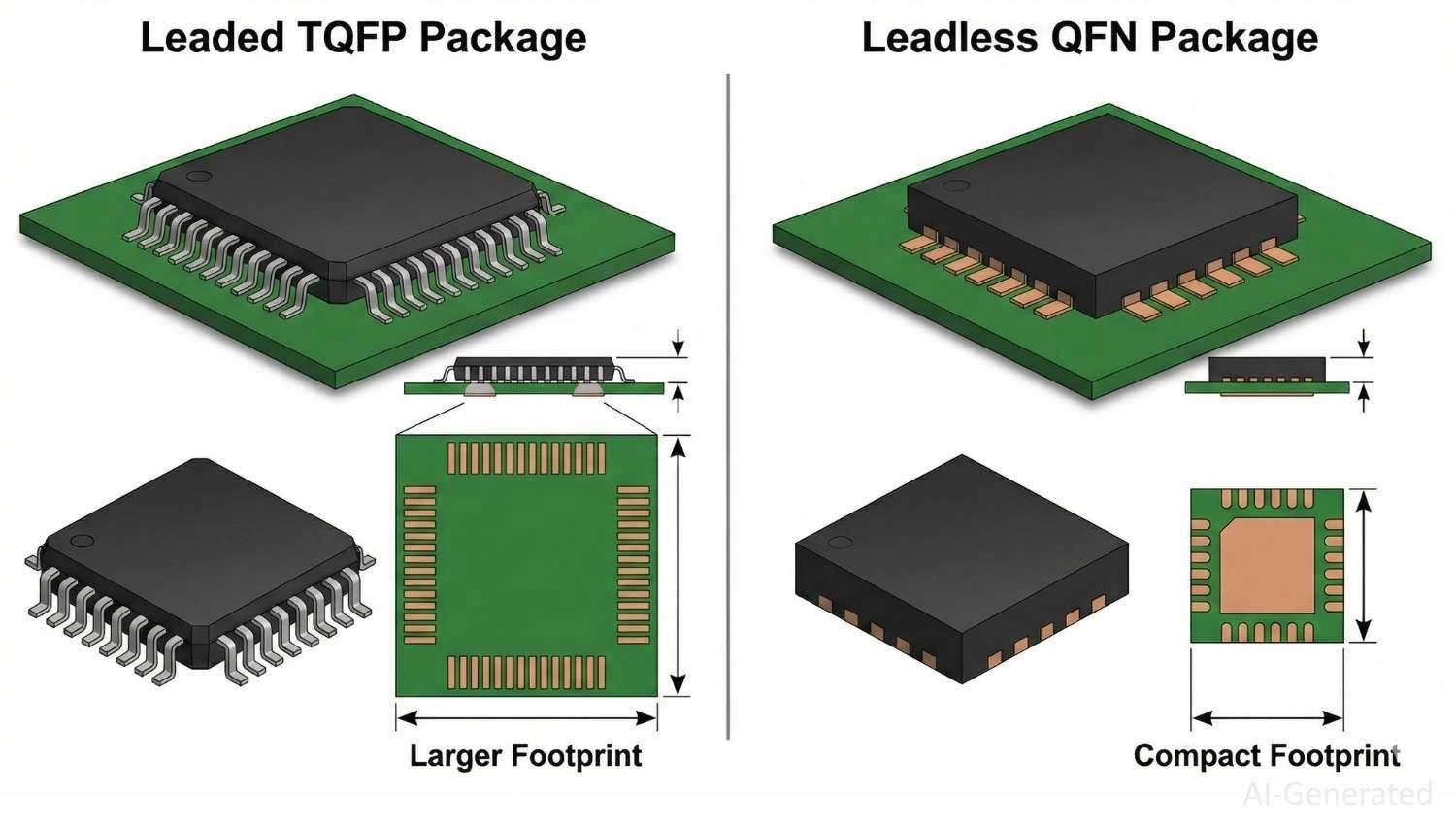
Footprint | Larger (takes more PCB area) | Compact/Minimalistic |
Thermal Pad | Usually No | Yes (Exposed Thermal Pad) |
Soldering | Easy (Hand-solder friendly) | Challenging (Reflow preferred) |
High-Speed/RF | Moderate (higher inductance) | Excellent (low parasitic inductance) |
Inspection | Visual/Optical | X-Ray often required |
Physical Size and PCB Footprint
The most immediate difference lies in the **PCB footprint and package geometry**.
TQFP packages use gull-wing leads that extend outward from the package body, significantly increasing the required board space and routing area.
In contrast, QFN is a near chip-scale package (CSP). With all contacts located underneath the package, its footprint is typically **40% to 60% smaller** than an equivalent TQFP with the same pin count.
For space-constrained designs—such as wearables or compact IoT devices—QFN provides a clear advantage due to its compact footprint and higher packaging density.
Thermal Performance
When it comes to heat dissipation, QFN holds a massive advantage. Most QFN packages include an exposed thermal pad (EPAD) on the bottom. This pad is soldered directly to the PCB ground plane, creating a low-resistance thermal path that pulls heat away from the silicon die.
TQFPs generally lack this feature, relying on the leads and the plastic body for cooling. For high-power applications or chips that run hot (like motor drivers or power management ICs), QFN prevents thermal throttling and improves longevity.
Electrical Performance
For high-frequency or RF designs, the "leads" on a TQFP act as tiny inductors and antennas, introducing parasitic inductance and capacitance that can degrade signal integrity.
Because QFN packages eliminate long leads, they offer a much shorter electrical path between the die and the PCB. This results in superior signal integrity and lower noise, making QFN the industry standard for high-speed digital circuits and wireless communication modules.
PCB Soldering and Assembly
This is where TQFP shines. Hand-soldering a TQFP is relatively straightforward for a skilled technician with a fine-tip iron because the leads are accessible. It is also more forgiving of "solder bridging" since you can easily see and wick away excess solder.
QFN assembly is more complex. Because the pads are tucked underneath, it typically requires a solder paste stencil and a reflow oven (or hot air station). Furthermore, the large thermal pad in the center can sometimes cause the chip to "float" if too much paste is applied, leading to connectivity issues on the outer signal pins.
Note
While QFN packages offer immense technical benefits, their bottom-pad design makes them a nightmare for hand-soldering. To avoid costly bridging and poor connectivity, many engineers now leverage JLCPCB’s SMT Assembly service.
With high-precision automated pick-and-place machines and specialized solder paste stencils, you can have your QFN components professionally mounted, eliminating the risks of manual prototyping.
Inspection and Rework
Post-assembly inspection is the final hurdle.
- TQFP: You can verify every solder joint using a standard microscope or even a high-powered magnifying glass.
- QFN: The solder joints are mostly hidden beneath the package. While side-fillets can sometimes be seen, a truly reliable inspection (especially for aerospace or medical grades) requires X-ray inspection to check for voids under the thermal pad or hidden bridges.
Reworking a QFN is also more destructive, usually requiring a specialized hot-air rework station, whereas a TQFP can often be touched up with a simple soldering iron.
What is a TQFP Package?
The TQFP (Thin Quad Flat Pack) is a surface-mount IC package that has been an industry workhorse for decades. As a "thin" evolution of the standard QFP, it was designed to provide a lower profile for devices where vertical space is limited, typically featuring a package thickness of 1.0 mm or 1.4 mm.
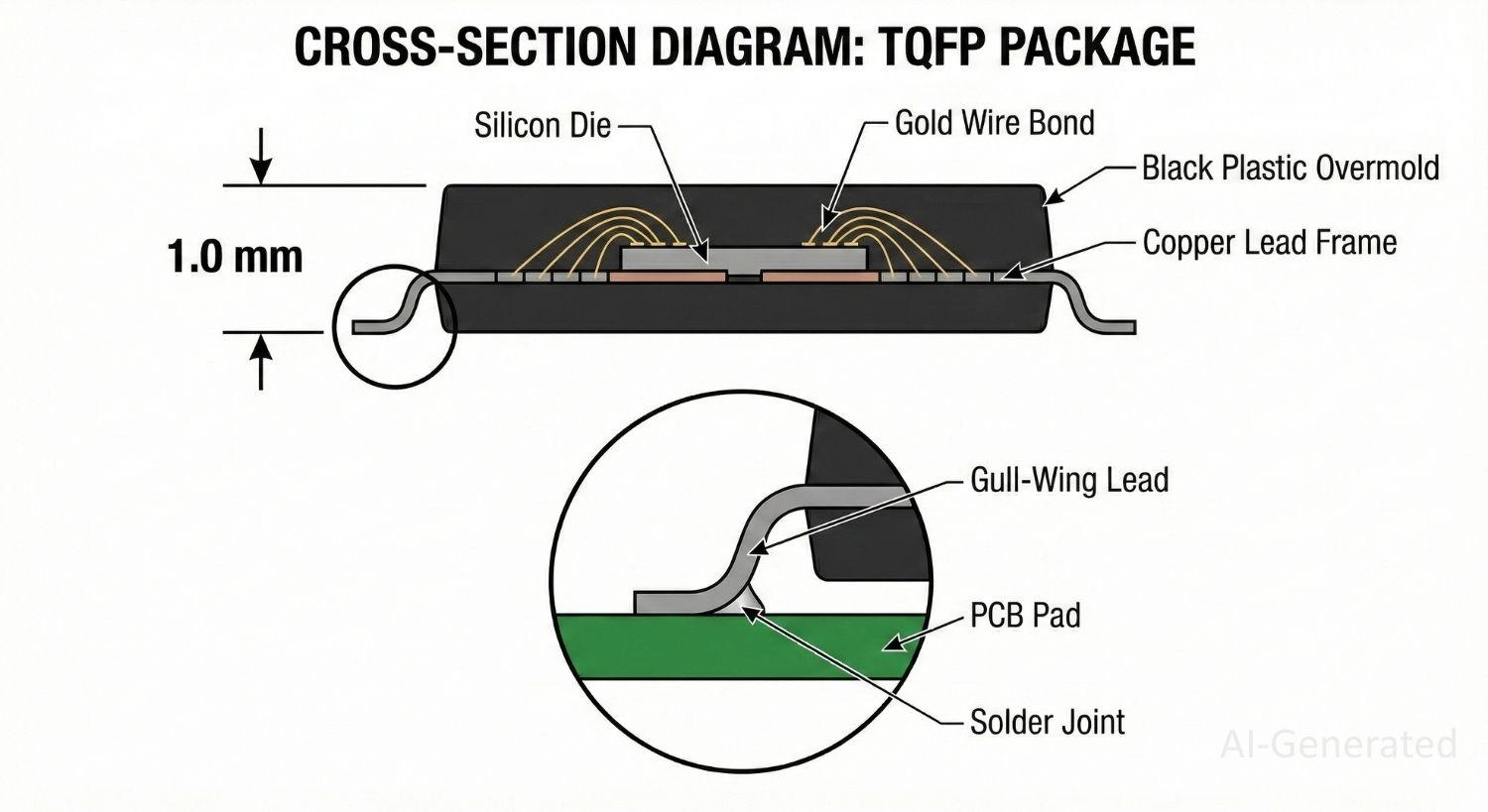
TQFP Structure: The Gull-Wing Lead
The defining characteristic of a TQFP is its gull-wing leads. These are metal pins that extend horizontally from all four sides of the plastic body and then curve downward and outward, resembling the wings of a seagull.
Unlike "no-lead" packages, these pins provide a visible, flexible mechanical connection to the PCB. This structure allows the package to absorb some level of thermal expansion and mechanical stress, reducing the risk of solder joint cracking over time.
Key Features of TQFP Package
- Easy Visual Inspection: Because the leads are external and clearly visible, engineers can verify solder joint quality using a standard microscope or AOI (Automated Optical Inspection) without needing X-ray equipment.
- High Pin Count Flexibility: TQFPs are available in a wide range of pin counts, typically from 32 to over 200 pins, making them adaptable for complex integrated circuits.
- Design-Friendly Pitch: While the lead pitch can be fine (down to 0.4 mm or 0.5 mm), the leads are still large enough for manual probing during the debugging phase of a project.
- Ease of Rework: If a chip is faulty, it can be removed and replaced relatively easily with a standard hot-air station and a steady hand.
Typical Applications of TQFP Package
TQFP packages are the "go-to" choice for general-purpose electronics where extreme miniaturization isn't the primary goal, but reliability and ease of manufacturing are.
- Microcontrollers: Most famously used in the Atmel/Microchip ATmega series (the heart of many Arduino boards) and various ARM Cortex-M processors.
- Consumer Electronics: Found in household appliances, digital clocks, and older generations of gaming consoles.
- Industrial Controllers: Preferred in environments where vibration or thermal cycling might cause "stiffer" packages to fail.
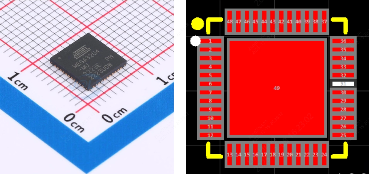
What is a QFN Package?
The QFN (Quad Flat No-leads) package represents a shift toward modern miniaturization. Unlike the TQFP, which uses external pins, the QFN connects to the PCB via flat copper pads located on the bottom surface of the package body. This "leadless" design allows the chip to sit closer to the board, significantly reducing its overall profile and volume.
QFN Structure: Bottom-Pads and the EPAD
The structure of a QFN is defined by its perimeter land pads and a large, central Exposed Thermal Pad (EPAD).
- Perimeter Pads: These are located along the four edges of the bottom of the package. Since there are no leads extending outward, the package footprint is nearly identical to the size of the silicon die itself.
- Exposed Pad (EPAD): This is the "secret sauce" of the QFN. It is a large metal area on the bottom that is soldered directly to the PCB. It serves two purposes: it acts as a high-efficiency heat sink and provides a solid electrical ground connection.
Key Features of QFN Package
- Ultra-Compact Footprint: Because the leads don't "splay" out like a TQFP, QFNs save a massive amount of PCB space. This allows for higher component density in complex designs.
- Superior Thermal Dissipation: The direct metal-to-metal contact between the EPAD and the PCB ground plane allows for much lower thermal resistance. This makes QFNs ideal for chips that generate significant heat.
- Lower Lead Inductance: Without long, wire-like leads, the electrical path from the die to the board is extremely short. This minimizes parasitic inductance, which is critical for maintaining signal integrity in high-frequency applications.
- Reduced Weight: The lack of heavy copper leads makes these packages ideal for weight-sensitive applications like drones or portable medical devices.
Typical Applications of QFN Package
QFN packages are the standard for high-performance electronics where every millimeter and milliwatt counts.
- RF and Wireless Modules: Used in Wi-Fi, Bluetooth, and 5G chips where low inductance is required to handle gigahertz frequencies.
- Power Management ICs (PMICs): Voltage regulators and battery chargers use the thermal pad to stay cool while handling high currents.
- High-Speed Digital Circuits: Used in modern processors and high-speed data converters (ADCs/DACs) that require clean, low-noise signals.
- Automotive Sensors: Their low profile and robust thermal connection make them a favorite for compact automotive control units.
Key Factors to Consider When Choosing TQFP vs QFN
Choosing between TQFP and QFN is a technical decision that impacts your manufacturing yield, product size, and long-term reliability.
Here are the four critical factors you should weigh before finalizing your BOM (Bill of Materials).
#1 Space Constraints: How Small is Your Board?
If you are designing for wearables, IoT sensors, or high-density mobile devices, QFN is the undisputed winner.
- The QFN Advantage: Because it lacks external leads, a QFN package can save up to 60% of the PCB real estate compared to a TQFP with the same pin count.
- The TQFP Reality: If you have plenty of "green space" on your board and aren't worried about every millimeter, TQFP is a perfectly fine, robust choice.
#2 Prototyping Needs: Are You Hand-Soldering?
In the early stages of a project, the "human factor" matters.
- Pick TQFP if: You are building prototypes in a lab or your office. Its visible gull-wing leads are easy to solder with a standard fine-tip iron, and if you accidentally bridge two pins, a bit of solder wick fixes it in seconds.
- Avoid QFN if: You don't have access to a reflow oven or a high-quality hot air station. Soldering a QFN by hand is a "dark art" that often leads to poor connectivity on the hidden pads or a tilted chip that’s impossible to debug without an X-ray.
#3 Thermal Dissipation: Does the Chip Run Hot?
Heat is the enemy of silicon. If your IC is a power-hungry microcontroller or a motor driver, you need a way to move that heat into the PCB.
- Pick QFN for High Heat: The Exposed Thermal Pad (EPAD) on the bottom of a QFN acts as a direct thermal highway. When soldered to a copper pour with thermal vias, it keeps junction temperatures significantly lower.
- TQFP Limitations: Most standard TQFPs dissipate heat primarily through their plastic body and thin leads, which is much less efficient. If your TQFP chip is running hot, you might need to add bulky external heatsinks.
#4 Signal Integrity: Dealing with GHz Frequencies
In the world of high-speed digital and RF (Radio Frequency), every millimeter of wire acts like an inductor.
- Pick QFN for Performance: The "no-lead" design means the distance from the internal die to the PCB trace is as short as possible. This minimizes parasitic inductance, which is essential for stable performance in the 1 GHz to 5 GHz+ range.
- TQFP for Low-Speed: For standard 16 MHz or 48 MHz microcontrollers, the inductance of TQFP leads is negligible. However, for modern high-speed communication, those leads can become "antennas" that introduce unwanted noise.
Practical PCB Design Tips for TQFP and QFN
While TQFP is more forgiving in layout and assembly, QFN demands tighter control over footprint design and heat dissipation. The following practical tips will help improve manufacturability, yield, and long-term reliability.
Fan-out Strategies for High-Pin-Count TQFPs
TQFP packages expose leads on all four sides, making them relatively easy to route compared to leadless packages. However, high pin counts (e.g., 100+ pins) can still create routing congestion.
Best practices:
1. Use dog-bone fan-out routing
Route traces outward from each pad before transitioning to inner layers via vias. This helps avoid trace overlap near the pad edges.
2. Optimize trace width and spacing early
Ensure your design rules match your PCB manufacturer’s minimum trace/space capability to prevent late-stage redesign.
3. Leverage multiple routing layers
For high-density TQFPs, use at least 4-layer boards to separate signal, power, and ground routing efficiently.
4. Group signals logically
Route power, ground, and high-speed signals in organized groups to reduce crosstalk and simplify debugging.
5. Common mistake to avoid:
Overcrowding traces near pad exits, which can lead to manufacturing defects or impedance inconsistencies.
The Importance of Thermal Vias for QFN Packages
QFN packages rely heavily on the exposed thermal pad underneath the component for heat dissipation. Without proper thermal design, overheating and reliability issues can occur.
Key design guidelines:
1. Place multiple thermal vias under the exposed pad
Use an array of vias to transfer heat from the top layer to internal or bottom copper planes.
2. Via diameter and pitch optimization
Typical via diameter: 0.2–0.3 mm
Keep spacing tight enough for heat transfer, but manufacturable.
3. Use via-in-pad with tenting or filling (if possible)
Tented vias prevent solder wicking
Filled vias improve reliability but increase cost
4. Connect to solid ground planes
Thermal vias should connect to large copper areas for effective heat spreading.
Why it matters:
QFN packages have no leads for heat conduction—the thermal pad is the only efficient heat path.
Solder Mask Design to Prevent Bridging
Solder bridging is a common issue in fine-pitch packages like TQFP and QFN, especially during reflow.
Design recommendations:
1. Use solder mask defined (SMD) pads for fine pitch
Helps control solder volume and reduces the risk of bridging between adjacent pins.
2. Maintain proper solder mask clearance
Avoid overly small mask openings that can trap solder or cause uneven wetting.
3. Segment the QFN thermal pad (windowpane design)
Divide the large center pad into smaller paste openings to:
- Prevent excessive solder
- Reduce floating or tilting during reflow
4. Control stencil thickness and aperture design
Proper stencil design ensures consistent solder paste deposition, which is critical for both TQFP leads and QFN pads.
5. Common defects caused by poor mask design:
- Solder bridges between pins
- Tombstoning or component misalignment
- Voiding under QFN thermal pad
Key Takeaway
1. TQFP: Focus on routing efficiency and fan-out strategy
2. QFN: Prioritize thermal management and solder control
3. Both: Require careful solder mask and stencil design to ensure assembly yield
Note
Component Sourcing: Before finalizing your design, check the JLCPCB Parts Library, which stocks thousands of TQFP microcontrollers and QFN RF chips in-house. Selecting "Basic Parts" from the Parts Library can significantly reduce your assembly lead time and overall BOM cost.
Conclusion: Making the Right Choice Between TQFP and QFN
Choosing between TQFP and QFN ultimately comes down to a trade-off between ease of assembly and performance optimization.
TQFP (Thin Quad Flat Package) remains the preferred choice for:
- Prototyping and low-volume production
- Designs requiring easy inspection and rework
- Engineers prioritizing simplicity and manufacturing robustness
QFN (Quad Flat No-lead) is better suited for:
- High-performance and high-frequency applications
- Compact designs with strict space constraints
- Systems requiring efficient thermal dissipation
From a PCB assembly perspective, TQFP offers a wider process window and lower risk, while QFN delivers superior electrical and thermal performance at the cost of tighter design and manufacturing control.
Final Recommendation:
- Choose TQFP for ease of use, debugging, and cost-sensitive projects.
- Choose QFN for performance-driven, space-constrained, and thermally demanding designs.
Ready to bring your TQFP or QFN design to life? Upload your Gerber files to JLCPCB today to get an instant quote on high-quality PCBs and professional SMT assembly. With 24-hour turnaround times and global shipping, JLCPCB makes advanced IC packaging accessible to every engineer.
Frequently Asked Questions
Q: Can QFN be hand-soldered?
Yes, QFN packages can be hand-soldered, but it is significantly more challenging than TQFP.
Because QFN components have no exposed leads and rely on pads underneath the package, traditional soldering methods are not sufficient. Successful hand soldering typically requires hot air rework stations, solder paste (not just wire solder) and proper preheating and temperature control
Even with the right tools, inspection is difficult without X-ray, making QFN less suitable for manual assembly or prototyping.
Q: Is QFN more reliable than TQFP?
It depends on the application. For high-speed, high-power, or compact designs, QFN is generally more reliable. For mechanically sensitive or easily serviceable systems, TQFP may be the safer choice.
Q: Which is cheaper, TQFP or QFN?
In most cases, TQFP is more cost-effective for prototyping and small batches, while QFN becomes competitive in high-volume manufacturing.
Popular Articles
• SMD Resistor Package Sizes: Complete Size Chart, Footprints & How to Choose
• SMD Capacitor Codes: Identification, Markings, and Polarity
• SMD Capacitor Sizes: Complete Size Chart and Selection Tips for PCB Design and Assembly
• How to Solder SMD Components Like a Pro [2026 Updated]
• The Complete Guide to Read SMD Resistor Codes
Keep Learning
PoP Package (Package on Package) Explained: Architecture, Assembly, and SMT Challenges
In the race for miniaturization, fitting more processing power into smaller footprints is the ultimate challenge for PCB designers. Package on Package (PoP) technology answers this by integrating logic and memory vertically, becoming the standard for modern mobile processors. However, this 3D architecture demands advanced SMT assembly capabilities beyond standard fabrication. JLCPCB specializes in the high-precision manufacturing required to master these complex stacks. This guide covers how PoP packa......
What Is a PQFP Package? Plastic Quad Flat Package Design, Footprint, and Assembly Guide
The Plastic Quad Flat Package (PQFP) is a widely used IC package in industrial, automotive, and embedded designs. This article provides a practical, engineering-focused guide to PQFP package. It explains how PQFP is built, when it makes sense to use it, how it compares with newer package types, and what designers should consider in terms of footprint design, thermal performance, signal integrity, manufacturing, and reliability. What Is a PQFP Package (Plastic Quad Flat Package)? A Plastic Quad Flat Pa......
Small Outline Integrated Circuit (SOIC): Package, Specs & Uses
As designs transition from legacy through-hole components to high-density Surface Mount Technology (SMT), the Small Outline Integrated Circuit (SOIC) remains the industry standard for operational amplifiers, flash memory, sensors, and microcontrollers. It stands as a testament to balanced engineering, offering a perfect compromise between the miniaturisation demanded by modern consumer electronics and the ruggedness required for industrial applications. This article serves as a definitive engineering ......
A Complete Guide to Surface Mount Device (SMD)
Imagine holding a smartphone in your hand. Inside that sleek device lies a complex network of thousands of miniature components — resistors smaller than a grain of rice, capacitors thinner than a fingernail, and integrated circuits containing millions of transistors. Without Surface Mount Technology (SMT) and its compact Surface Mount Devices (SMDs), none of this would exist. Just a few decades ago, electronics were bulky. Radios filled desks, computers filled rooms, and assembling a circuit meant dri......
Circuit Breaker Types Explained: MCB, MCCB, RCCB, RCBO, ACB, VCB & SF6 Circuit Breakers
A circuit breaker automatically disconnects power when it detects faults such as overloads or short circuits, protecting equipment and reducing fire risk. Different circuit breaker types are designed for different voltage levels, current ratings, and applications, from household distribution boards to high-voltage substations. This guide explains the most common types - including MCBs, MCCBs, RCCBs, RCBOs, ACBs, VCBs, and SF6 breakers and helps you choose the right one for your application. Figure: Ci......
Quad Flat Package (QFP): The Engineer's Guide to Design, Assembly and Thermal Management
What is QFP Package? The Quad Flat Package (QFP) is one of the most popular surface mount technology (SMT) package formats throughout the history of electronic manufacturing. After it became standard in the 1980s, the QFP has been the industry standard for integrated circuits (ICs) with moderate to high pin counts that typically range from 32 to 304 pins, so it was a good alternative for simple SOIC packages and complex Ball Grid Arrays (BGAs) at the same time. Defined by its "gull-wing" leads extendi......