
How to Use a BGA Stencil for SMT Assembly and Reballing (Design & Process Guide)
6 min
- Quick Answer: BGA Stencil Design & Selection Guide
- Method 1: Using a PCB Stencil for Initial BGA Assembly
- Method 2: Using a BGA Reballing Stencil to Restore Chips
- Troubleshooting BGA Defects Caused by Stencil Errors
- How to Order Precision BGA Stencils from JLCPCB
- Frequently Asked Questions about BGA Stencil
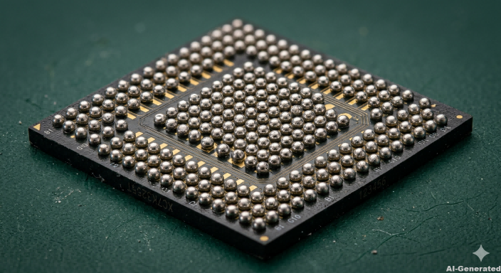
Anyone who's spent time in a lab knows the look. You flip over a BGA chip and stare at the bottom. Flat. Featureless. No legs. No leads. Just a grid of tiny silver bumps.
First thought? How the hell am I supposed to solder this?
The Ball Grid Array (BGA) package is a trade-off. You get insane I/O density in a tiny footprint. But every single connection is hidden. You can't see them, and you can't poke them with an iron. Here's the thing I learned after lifting more pads than I'd like to admit: learning to work with BGA components isn't about having surgeon hands. It's about controlling solder volume.
The only tool that gives you that volumetric control is a precision BGA stencil. Once you've got the right stencil—whether for initial board assembly or chip reballing—BGA work stops feeling like gambling. It becomes a repeatable process.
Quick Answer: BGA Stencil Design & Selection Guide
To prevent bridging and voiding under BGA components, ensure your stencil meets these baseline parameters:
-
Stencil Thickness: Use 0.10 mm to 0.12 mm for standard BGA pitches (0.5 mm - 0.8 mm). Use 0.08 mm for ultra-fine pitch (0.4 mm).
-
Aperture Size: Design apertures to be 1:1 with the PCB pad, or slightly reduced (e.g., 90%) to prevent bridging.
-
Aperture Shape: Use round or slightly squircle (rounded square) apertures for optimal paste release.
-
Surface Finish: Always specify electropolishing or nano-coating to prevent paste from sticking inside fine-pitch BGA holes.
Method 1: Using a PCB Stencil for Initial BGA Assembly
When assembling a fresh board, you use a standard SMT board-level stencil to deposit paste onto the bare PCB pads before placing the BGA chip.
1Step 1: Board Prep
Clean the PCB pads with isopropyl alcohol (IPA). Any fingerprint oils or dust will cause the solder to reject the pad.
2Step 2: Solder Paste Application
This is where you make or break the board.
-
Secure your PCB.
-
Align the PCB stencil perfectly. BGA pitch is unforgiving; half a millimeter off, and you're printing paste onto the solder mask.
-
Apply solder paste (SAC305 for lead-free, Sn63Pb37 for leaded) across the top.
-
Hold your squeegee at a 45-degree angle. Use firm, even pressure. One smooth swipe.
-
Lift the stencil straight up. You should see perfect, tiny cylinders of paste on every pad.
3Step 3: Component Placement
The paste acts like a weak glue. Carefully place the BGA chip onto the pasted pads. You don't need sub-micron accuracy here. The beauty of BGA is that during reflow, the surface tension of the molten solder will actually pull the chip into perfect alignment. Just get it close and square to the silkscreen.
4Step 4: Reflow
Run the board through your reflow oven following the paste manufacturer's profile. You need a proper soak zone to activate the flux, followed by a spike to liquidus.
Method 2: Using a BGA Reballing Stencil to Restore Chips
Sometimes you have to pull a dead chip or salvage an expensive FPGA. When you pull a BGA, the solder balls are destroyed. To reuse the chip, you have to apply new spheres. This requires a specialized BGA reballing stencil.
The Reballing Process:
- Prep: After removing the chip and cleaning the old solder flat with wick, clean the chip with IPA.
- Apply Tacky Flux: Brush a very thin, even layer of tacky flux over the chip's pads. Too much flux, and the balls will boil away during heating.
- Align the Reballing Stencil: Place the BGA reballing stencil over the chip. Some people use direct-heat stencils; others use a jig.
- Apply Paste or Balls: You can wipe solder paste into the stencil holes, or pour solid solder spheres (balls) over the stencil, brushing them until one drops into every hole.
- Reflow: Heat the assembly with hot air. Watch the paste or balls melt and snap onto the pads. Let it cool, remove the stencil, and clean the flux residue. You now have a fresh chip.
Troubleshooting BGA Defects Caused by Stencil Errors
When a BGA fails, it's usually because the stencil process wasn't controlled.
-
Shorts (Bridging)
Usually caused by a stencil that is too thick, or squeegee pressure that was too high, forcing paste under the stencil foil.
-
Voids (Bubbles in the joint):
Often caused by expired solder paste or a reflow profile that heated up too fast, trapping flux gas before it could escape.
-
Head-in-Pillow (HiP):
The solder paste melts, but doesn't fuse with the BGA ball. This looks like a head resting on a pillow. It's typically caused by board warpage, oxidized balls, or insufficient paste volume deposited by a clogged stencil aperture.
How to Order Precision BGA Stencils from JLCPCB
BGA assembly leaves zero room for error. A cheap, poorly cut stencil with burrs will trap solder paste, leading to missing joints and dead boards.
To ensure clean paste release on fine-pitch BGAs, professional labs rely on stencils manufactured via high-precision laser cutting. JLCPCB provides industrial-grade custom stencils with advanced options like electropolishing and nano-coating, which are essential for BGA work.
You can order a custom precision stencil starting at just $3 USD, with production completed in as fast as 12 hours.
Frequently Asked Questions about BGA Stencil
Lead-free vs leaded. Which is easier to learn on?
Leaded. Sn63Pb37 melts clean at 183°C. SAC305 is a pasty mess that peaks around 240°C. Higher temps mean more warpage and more voids. If you're new, use leaded paste and leaded balls.
Do I need a $2,000 rework station?
For 0.4mm and 0.5mm pitch on dense boards? Honestly, yeah. The optical alignment on a proper BGA station makes placement possible. For 0.8mm and larger, a good hot air station and a pre-heater plate will get you there with patience.
How do I know if it worked without X-ray?
Power it up. If it passes functional test and doesn't short, you're probably fine. For anything mission-critical, send it out for X-ray. It's the only way to see voiding or marginal joints under the chip.
BGA assembly can be intimidating, especially when every connection is hidden beneath the chip. But as we've explored, it isn't magic. It's about controlling the variables you can measure—stencil thickness, aperture design, and paste volume—so the hidden joints form perfectly every time.
Trust the physics. With a precision BGA stencil, clean surfaces, and the right heat profile, the solder naturally wants to form good joints. By removing the guesswork from your paste deposition, you transform a risky, frustrating process into a repeatable success.
Keep Learning
Manual Pick and Place: A Cost-Effective SMT Alternative
Key Takeaways for Manual Pick and Place Manual pick and place uses a hand-held vacuum wand and positioning stage to place SMD components by hand, replacing tweezers in prototype assembly. It is most cost-effective for production runs of 1 to 50 boards, where an automated SMT pick-and-place machine cannot justify its $10,000+ setup cost. A complete manual workstation runs $300 to $500, compared with $10,000+ for an entry-level automated pick and place machine. SMT stencil quality is the single largest ......
Hot Air Surface Mount Soldering: A Step-by-Step Guide
Key Takeaways Heat Control Is Everything: Hot air SMD soldering delivers uniform heat across all pads simultaneously, eliminating the lifted pads and cold joints common with iron-based soldering of fine-pitch components. Airflow Kills Small Parts: Set airflow to just 10–20% for 0402/0201 passives to avoid the Bernoulli Effect that turns tiny resistors into projectiles. Stencil Precision Prevents Tombstoning: A precision-cut SMT stencil deposits equal paste volume on both pads, balancing surface tensio......
Solder Paste Printing Defects: How Precision Stencils Prevent Assembly Failures
Key Takeaways 70% Rule: Approximately 70% of SMT defects originate from the solder paste printing stage, making it the most critical process to optimize. Root Causes: Defects like bridging, insufficient paste, misalignment, and slumping are caused by stencil tension, process parameters (pressure, speed), and paste chemistry/environment. Area Ratio Matters: Maintaining an aperture Area Ratio (AR) above 0.66 (per IPC-7525) is essential to ensure proper paste transfer efficiency and prevent chronic insuf......
Best Manual Pick and Place Tools for Precise PCB Assembly
While fully automated robotic SMT lines handle mass production efficiently, every hardware innovation begins on a workbench. Engineers shifting from soldering large through-hole components to microscopic surface-mount devices (SMD) by hand quickly realize that precision and control are everything. Achieving factory-level assembly on your desk is absolutely possible with the right setup. This guide reviews the essential tool categories needed to build an effective prototyping workbench, covering precis......
How to Use a BGA Stencil for SMT Assembly and Reballing (Design & Process Guide)
Anyone who's spent time in a lab knows the look. You flip over a BGA chip and stare at the bottom. Flat. Featureless. No legs. No leads. Just a grid of tiny silver bumps. First thought? How the hell am I supposed to solder this? The Ball Grid Array (BGA) package is a trade-off. You get insane I/O density in a tiny footprint. But every single connection is hidden. You can't see them, and you can't poke them with an iron. Here's the thing I learned after lifting more pads than I'd like to admit: learnin......
Solder Bead Prevention: How PCB Stencil Design & Process Control Deliver Defect-Free Reflow Soldering
In modern SMT assembly, solder joint quality is determined long before the reflow oven starts—at the solder paste printing stage. When this step is not properly controlled, the consequences appear after reflow as tiny spherical solder particles scattered around component pads: solder beads. For engineers working with high-density assemblies, these defects are familiar and frustrating because they reappear whenever a process variable drifts outside its optimum range. This guide takes an engineering-fir......