
Solder Bead Prevention: How PCB Stencil Design & Process Control Deliver Defect-Free Reflow Soldering
9 min
- Quick Answer: How to Prevent Solder Beads
- What Are Solder Beads and What Causes Solder Beads in SMT Assembly?
- How to Prevent Solder Beads Through PCB Stencil Design
- Process Optimization for Solder Bead Prevention
- Troubleshooting Solder Beads in Production
- Frequently Asked Questions about PCB Stencils
In modern SMT assembly, solder joint quality is determined long before the reflow oven starts—at the solder paste printing stage. When this step is not properly controlled, the consequences appear after reflow as tiny spherical solder particles scattered around component pads: solder beads.
For engineers working with high-density assemblies, these defects are familiar and frustrating because they reappear whenever a process variable drifts outside its optimum range. This guide takes an engineering-first approach to solder bead prevention, focusing on root causes, high-precision stencil design principles, and process optimization.
Quick Answer: How to Prevent Solder Beads
If you are looking for immediate ways to prevent solder beads in your SMT assembly, focus on these critical process controls:
-
Optimize Stencil Apertures: Reduce aperture size to 80–90% of the pad area, especially for chip components.
-
Upgrade Stencil Surface Finish: Use electropolishing or nano-coating to ensure clean solder paste release.
-
Control the Environment: Maintain workshop humidity below 60% to prevent moisture absorption in the flux.
-
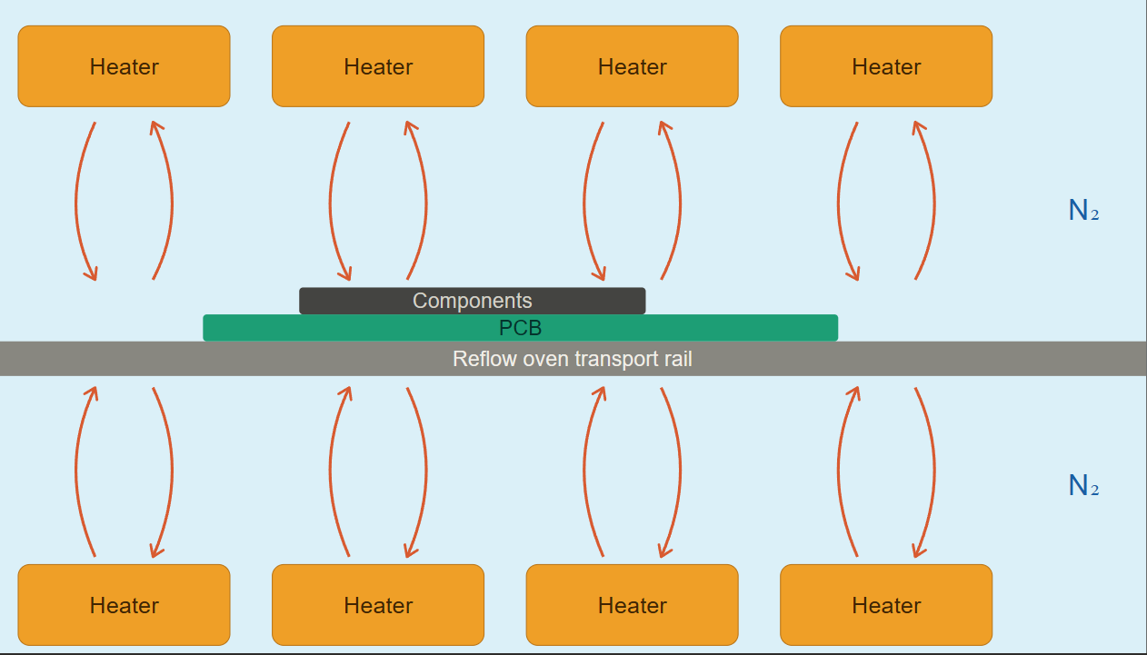
Manage Paste Profile: Ensure the reflow ramp rate remains under 3 °C/s to avoid solvent spattering.
-
Choose the Right Paste: Type 4 or Type 5 solder paste improves print definition for fine-pitch assemblies, indirectly reducing excess paste spread and bead formation.
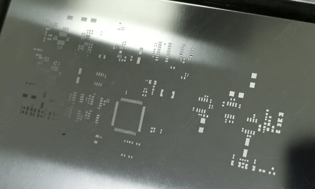
A critical first step in implementing these preventions is using a high-quality PCB stencil. JLCPCB offers custom stencils manufactured via high-precision laser cutting, which are essential for controlling solder paste volume.

What Are Solder Beads and What Causes Solder Beads in SMT Assembly?
What Are Solder Beads?
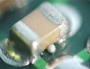
Solder beads are solidified spherical solder particles that form outside the intended pad area after reflow. They typically range from 0.05 mm to 0.5 mm and appear around component pads, near solder mask edges, or trapped beneath low-standoff components like chip resistors and capacitors.
The mechanism: excess solder paste or paste that migrates beyond the pad boundary separates from the main joint under surface tension and solidifies into a bead. Solder beads are often considered a subtype of solder balls, but in SMT troubleshooting they usually refer to larger particles formed around component edges.
Why Solder Beads Form
Solder bead formation is rarely due to a single factor. Common contributors include:
-
Excess solder paste deposition – from oversized apertures, excessive stencil thickness, or paste slumping.
-
Solder paste slumping – low viscosity, high ambient temperature, or paste beyond its working life causes lateral spread, reaching mask edges or component bodies.
-
Moisture absorption – flux is hygroscopic. Humidity > 60% or long open-jar times leads to steam spattering during reflow.
-
Aggressive reflow profile – ramp rates > 3 °C/s can volatilize solvents too quickly, causing spatter and poor wetting.
-
Poor pad-to-mask clearance – insufficient solder mask expansion (aim for 0.05–0.1 mm) allows paste entrapment under the mask edge.
How to Prevent Solder Beads Through PCB Stencil Design
The PCB stencil is your primary tool for controlling solder paste volume and placement. A well-designed stencil reduces slumping and directly prevents solder beads during the reflow process.
Optimizing Stencil Apertures for Defect Prevention
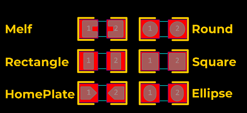
Stencil aperture design controls how solder paste is deposited onto PCB pads, directly impacting solder joint quality and reliability. Effective design goes beyond simply matching pad shapes; it often involves strategically adjusting aperture geometry and size to optimize paste volume and release. For instance, apertures are commonly made slightly smaller than the pad area to prevent paste from overflowing and causing bridging. Designers may use rounded rectangles or home plate shapes for small chip components, or circular apertures for fine-pitch arrays, ensuring paste distributes evenly while minimizing trapped paste and solder bead formation.
Optimizing Area and Aspect Ratios for Reliable Paste Transfer
Reliable paste transfer requires attention to key stencil design ratios. The area ratio, the aperture opening area divided by its total wall surface area, should remain above a critical threshold to ensure paste releases cleanly, especially on fine-pitch devices. It is calculated as:
Area Ratio = (L × W) ÷ [2 × (L + W) × T]
Where:
- L = aperture length
- W = aperture width
- T = stencil thickness
Maintaining an area ratio ≥ 0.66 supports consistent paste breakout. Similarly, an appropriate aspect ratio between aperture width and stencil thickness ensures smooth paste release. By balancing these ratios with careful aperture sizing and shape selection, designers can minimize defects such as bridging, tombstoning, and solder beads, achieving high-yield SMT assembly.
Selecting the Correct Stencil Thickness
Using a stencil that is too thick deposits excess paste, dramatically increasing the risk of beads. Step stencils allow for mixed thicknesses on a single tool if your board features both large connectors and ultra-fine pitch components.
| Thickness | Application | Bead Risk |
|---|---|---|
| 0.10 mm (4 mil) | Ultra-fine pitch (< 0.4 mm), 0201 | Low |
| 0.12 mm (5 mil) | Fine-pitch ICs (0.5 mm), 0402 | Low-medium |
| 0.15 mm (6 mil) | Mixed tech (0603+) | Medium |
| 0.20 mm (8 mil) | Large connectors, power | High for fine-pitch |
*Step stencils allow mixed thicknesses on one tool.
Choose from Framed/Frameless, Electropolishing, Nano-coating, Step-Stencils, SMD Glue Stencil and more. Starting at $3. No MOQ. 12-Hour production.
Get $11 Coupon Now >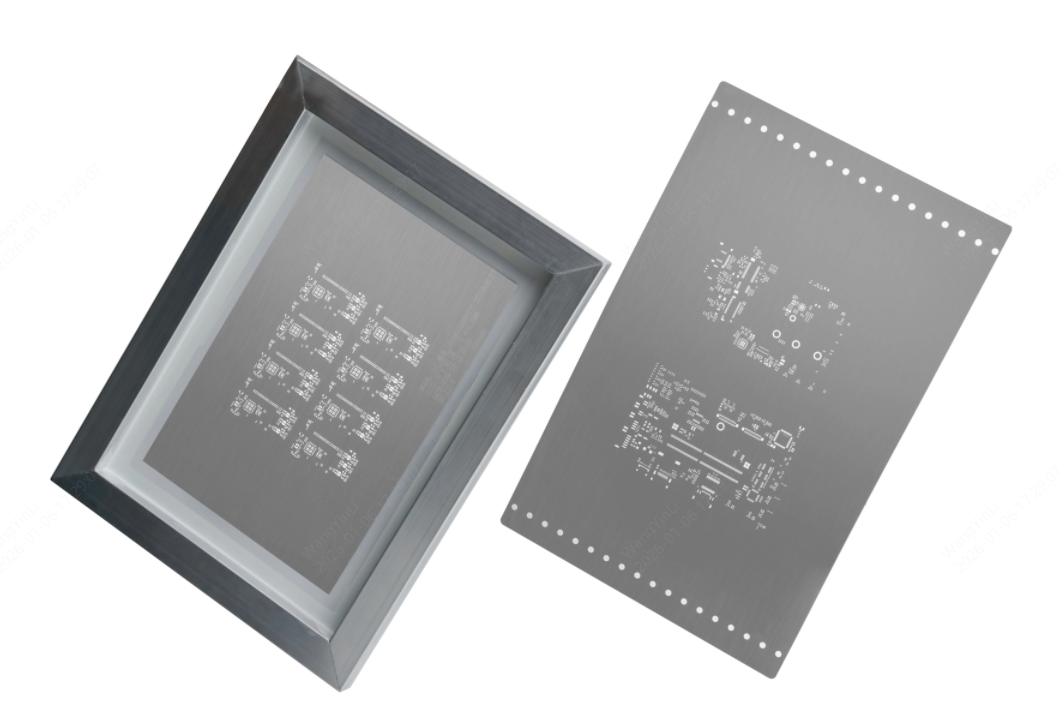
Utilizing Advanced Surface Finishes (Electropolishing & Nano-Coating)
The manufacturing process of the stencil directly impacts performance. While high-precision laser cutting creates accurate apertures, upgrading the surface finish further prevents defects:
- Electropolishing is an electrochemical finishing process that removes microscopic burrs and roughness created during laser cutting of stencil apertures. By smoothing the aperture walls, it improves solder paste release and reduces paste trapping or under-stencil buildup.
- Nano-coating applies an ultra-thin hydrophobic and oleophobic layer to the stencil surface and aperture walls. This low-friction coating reduces solder paste adhesion, improves paste transfer efficiency, and is especially beneficial for high-volume SMT printing and fine-pitch components.
- Some stencil manufacturers, such as JLCPCB, offer electropolished and nano-coated stencil options to further enhance paste release performance.
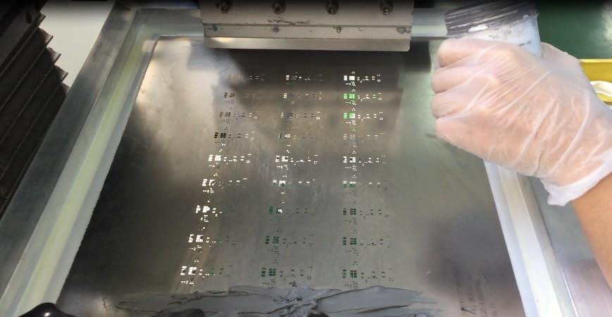
Process Optimization for Solder Bead Prevention
Even the perfect stencil requires strict process parameters.
-
Squeegee Control:
Maintain a speed of 20–55 mm/s. Use the minimum pressure needed for a clean wipe (0.1–0.3 N/mm); excess pressure scoops paste out and forces it under the stencil, causing beads.
-
Frequent Stencil Cleaning:
Clean every 5–10 print cycles using lint-free wipes and solvent. Automated printers can be programmed for consistent cycles. Effective cleaning removes both under-stencil smear (bead cause) and aperture clogging (insufficient solder).
-
Environment & Paste Management:
Store paste at 2–10 °C and allow ≥ 4 hours to reach room temperature before opening. Keep workshop humidity < 60%. Use Type 4 or Type 5 powder for modern mixed-tech assemblies.
Troubleshooting Solder Beads in Production
If solder beads still appear, use this quick diagnostic guide:
| Symptom | Root Cause | Corrective Action |
|---|---|---|
| Beads around 0402/0603 pads | Aperture too large / stencil too thick | Reduce aperture to 80–90%; consider 0.12 mm stencil. Monitor tombstoning. |
| Beads only at shift start | Cold paste, condensation | Equilibrate paste 4+ hours before opening. |
| Random beads across board | Moisture in flux | Humidity < 60%; replace old paste. |
| Beads increase during run | Under-stencil residue | Increase cleaning frequency; check squeegee pressure. |
| Beads under chip caps | Paste slumping beneath component | Home-plate apertures; higher viscosity paste. |
| Beads at mask edges (HASL) | Insufficient pad-to-mask clearance | Increase mask expansion to 0.075–0.1 mm. |
| Beads in mass production only | Process at limit, amplified at scale | Audit all variables: stencil, paste age, humidity, settings. |
Frequently Asked Questions about PCB Stencils
How can I reduce solder beads on fine-pitch ICs (<0.5 mm)?
Use solder paste with smaller particles (Type 4 for 0.5 mm pitch, Type 5 for finer), maintain stencil aperture area ratio ≥0.66, and adjust squeegee speed and pressure. Proper aperture shape and smooth release reduce bead formation.
Can stencil wear cause beads over time?
Yes. Worn apertures and under-stencil buildup reduce paste transfer and increase defects. Replace stencils when deposits become inconsistent or apertures deform.
Does board layout affect bead formation?
Absolutely. Close pad spacing, insufficient mask clearance, and poor pad-to-mask design trap paste and create beads. Optimize pad-to-mask clearance (0.05–0.1 mm) and avoid via-in-pad near fine-pitch devices.
Are certain solder pastes better for preventing beads?
Yes. Low-viscosity pastes with proper particle size (Type 4 or 5) improve aperture fill and reduce bead risk. Metal content around 88–90% and proper rheology also help.
How do environmental factors influence solder beads?
High humidity and temperature variations affect paste rheology, increasing bead risk. Keep the workshop stable (20–28 °C, <60% RH) and equilibrate paste before printing.
Can automated inspection detect solder beads reliably?
AOI can detect visible solder beads above the programmed inspection threshold. For very small beads or under-chip areas (e.g., BGA), X-ray inspection (AXI) is needed.
What are the risks of using HASL vs. ENIG for bead prevention?
HASL’s uneven surface can compromise stencil contact, increasing bead formation. ENIG is flatter, improving paste release and reducing beads, especially on fine-pitch designs.
How can hobbyists prevent solder beads without full SMT equipment?
Control paste exposure, use thin deposits, select proper particle size, clean stencils frequently, and print slowly. Avoid high humidity and long open-paste times.
Conclusion
Solder beads are preventable. Each root cause has an engineering solution. By utilizing a high-precision stencil with optimized apertures and appropriate surface finishes (like electropolishing or nano-coating), you create the widest possible process window, heavily reducing the chance of bead formation.
JLCPCB delivers high-quality stencils manufactured via high-precision laser cutting at the best price. Start optimizing your assembly today.
Keep Learning
Manual Pick and Place: A Cost-Effective SMT Alternative
Key Takeaways for Manual Pick and Place Manual pick and place uses a hand-held vacuum wand and positioning stage to place SMD components by hand, replacing tweezers in prototype assembly. It is most cost-effective for production runs of 1 to 50 boards, where an automated SMT pick-and-place machine cannot justify its $10,000+ setup cost. A complete manual workstation runs $300 to $500, compared with $10,000+ for an entry-level automated pick and place machine. SMT stencil quality is the single largest ......
Hot Air Surface Mount Soldering: A Step-by-Step Guide
Key Takeaways Heat Control Is Everything: Hot air SMD soldering delivers uniform heat across all pads simultaneously, eliminating the lifted pads and cold joints common with iron-based soldering of fine-pitch components. Airflow Kills Small Parts: Set airflow to just 10–20% for 0402/0201 passives to avoid the Bernoulli Effect that turns tiny resistors into projectiles. Stencil Precision Prevents Tombstoning: A precision-cut SMT stencil deposits equal paste volume on both pads, balancing surface tensio......
Solder Paste Printing Defects: How Precision Stencils Prevent Assembly Failures
Key Takeaways 70% Rule: Approximately 70% of SMT defects originate from the solder paste printing stage, making it the most critical process to optimize. Root Causes: Defects like bridging, insufficient paste, misalignment, and slumping are caused by stencil tension, process parameters (pressure, speed), and paste chemistry/environment. Area Ratio Matters: Maintaining an aperture Area Ratio (AR) above 0.66 (per IPC-7525) is essential to ensure proper paste transfer efficiency and prevent chronic insuf......
Best Manual Pick and Place Tools for Precise PCB Assembly
While fully automated robotic SMT lines handle mass production efficiently, every hardware innovation begins on a workbench. Engineers shifting from soldering large through-hole components to microscopic surface-mount devices (SMD) by hand quickly realize that precision and control are everything. Achieving factory-level assembly on your desk is absolutely possible with the right setup. This guide reviews the essential tool categories needed to build an effective prototyping workbench, covering precis......
How to Use a BGA Stencil for SMT Assembly and Reballing (Design & Process Guide)
Anyone who's spent time in a lab knows the look. You flip over a BGA chip and stare at the bottom. Flat. Featureless. No legs. No leads. Just a grid of tiny silver bumps. First thought? How the hell am I supposed to solder this? The Ball Grid Array (BGA) package is a trade-off. You get insane I/O density in a tiny footprint. But every single connection is hidden. You can't see them, and you can't poke them with an iron. Here's the thing I learned after lifting more pads than I'd like to admit: learnin......
Solder Bead Prevention: How PCB Stencil Design & Process Control Deliver Defect-Free Reflow Soldering
In modern SMT assembly, solder joint quality is determined long before the reflow oven starts—at the solder paste printing stage. When this step is not properly controlled, the consequences appear after reflow as tiny spherical solder particles scattered around component pads: solder beads. For engineers working with high-density assemblies, these defects are familiar and frustrating because they reappear whenever a process variable drifts outside its optimum range. This guide takes an engineering-fir......