
Achieving Stable Power Delivery : Mastering PDN Impedance in High-Performance PCBs
14 min
- Why PDN Impedance Is Critical for Modern PCB Designs
- Understanding Target Impedance and Its Importance
- Key Factors Influencing PDN Impedance
- Practical Techniques for PDN Impedance Analysis and Optimization
- Manufacturing Considerations for Low PDN Impedance
- JLCPCB's Expertise in PDN Impedance Optimized PCBs
- Conclusion
- FAQ about PDN Impedance
- Conclusion
Key Takeaways
- PDN impedance directly determines voltage stability under load. Keep it low and flat.
- Calculate your target: Z_target = (V_dd × Ripple%) / I_transient — typically single-digit milliohms.
- Prioritize close power-ground planes, short via connections, and strategic decoupling placement.
- Avoid anti-resonance peaks; a smooth curve matters more than raw capacitance.
- Precise manufacturing (copper thickness, dielectric control) is essential to match simulation results.
There's no point in using a gigahertz processor if it can't be powered by gigahertz power. You can route your high-speed signals flawlessly, match your differential pairs to within the picosecond, and still see your board acting up under load. In most cases, the problem is in the PDN, and more particularly in the PDN impedance that your starving ICs experience. I discovered this the hard way on a project in which an FPGA started dropping bits during intense compute bursts. The drawing was good. Signal Integrity was good. But when the device suddenly sucked a lot of power, the core rail drooped.
That sag was just a transient current through an impedance that was too high at that frequency. In this guide, I would like to take you through PDN impedance as I wish someone had done for me. We will discuss what it is, how to set a reasonable target impedance, what design and manufacturing factors affect it, and how to measure the actual value on the completed board. At the conclusion, you should be able to view a power rail and think like a PIE.
Why PDN Impedance Is Critical for Modern PCB Designs
Each time that the switch occurs (millions or billions of times a second in every digital IC), it pulls a little charge from the power rail. If all the gates switch simultaneously, the current demand is very sudden and intense. The PDN's task is to provide this charge as smoothly as possible without much voltage disturbance. The impedance of the network that supplies the chip is high at the frequencies at which the chip consumes current, and you get voltage noise. That noise reduces timing margins, affects signal integrity, and can even result in complete functional failure. This is even more difficult with modern low-voltage devices.
What PDN Impedance Means and Its Role in Power Integrity
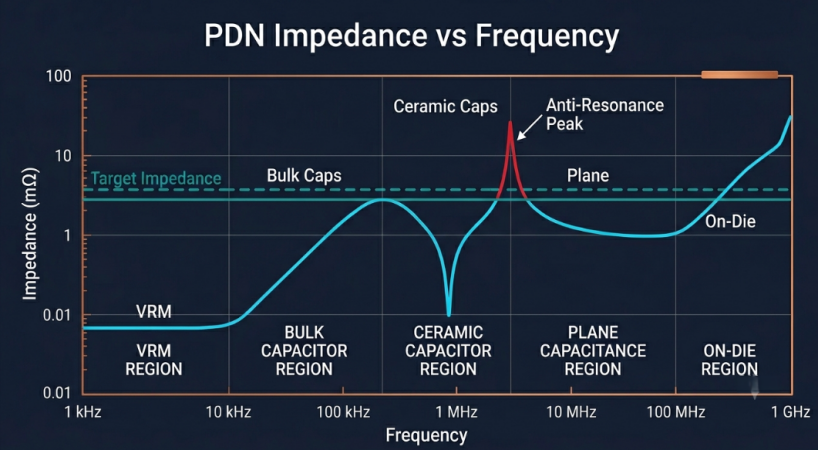
The PDN is the entire path that delivers power from your voltage regulator module (VRM) to the silicon die, copper planes, vias, decoupling capacitors, package, and on-die capacitance, all included. PDN impedance is just the impedance this network offers to the load vs. frequency. The thing is, it isn't a number. It is a curve, Z(f), which varies greatly over the spectrum. But at very low frequencies, the VRM dominates, and the impedance is very small.
Control loops cannot operate at high frequencies, so there are bands where bulk capacitors operate, bands where ceramic capacitors operate, bands where plane capacitance operates, and bands where on-die capacitance operates. The entire Power Integrity dance is to keep this curve low and flat in the frequency region where your load consumes current. Once you get this right, you have a quiet rail. If you don't, noise infiltrates just where you don't want it.
The Impact of High PDN Impedance on Voltage Stability and Performance
The formula is simply: the voltage noise is equal to the transient current times the impedance. With a 10mΩ impedance, 5A step current creates 50mV of ripple — and that's 3% of the 1.0V core rail with a 3% budget. High PDN impedance manifests itself in a number of ugly ways:
- More voltage ripple and droop during load transients
- Smaller timing margin for high-speed interfaces (such as DDR and SerDes interfaces)
- Increased jitter on clocks and PLL-generated signals.
- EMI is increased with the noisy rail coupled to other structures
- Occasionally, difficult to diagnose functionality issues during peak usage
The frequencies at which the spikes in impedance are significant. Even if a curve is otherwise nice, a single sharp peak at 30 MHz can destroy a design. Hence, the importance of the overall profile and not only DC resistance.
Understanding Target Impedance and Its Importance
You must have a goal before you can optimize a PDN. The target impedance is the maximum allowable impedance in your network for the band of frequencies of interest. Don't cross it anywhere, and your rail noise remains affordable. It is one of those fuzzy 'make the power clean' concepts that can be converted into a tangible engineering specification that can be designed and tested against.
Defining PDN Target Impedance for Different Applications
The classic formula for PDN target impedance is straightforward:
Z_target = (V_dd × allowed_ripple%) / I_transient
Where V_dd is the rail voltage, allowed_ripple% is your noise budget as a fraction, and I_transient is the worst-case transient current the load can demand.
Let's take an actual example: There is a 1.0 V core rail that has a 5% ripple allowance and a 10A transient. That gives Z_target = (1.0 × 0.05) / 10 = 5 mΩ. Now you have to ensure that the impedance is < 5mΩ, spanning a range from DC to tens and/or hundreds of MHz.
How Target Impedance Affects Transient Response and Noise
The target impedance is really a frequency domain approximation of the time domain behavior. If Z(f) is flat and below target, then the rail responds cleanly to any current step within your assumed bandwidth. Anti-resonance peaks are where the danger lies. The impedance rises at a certain frequency when the inductance of one decoupling stage resonates with the capacitance of the other. If this peak is above your target line, then the nasty voltage excursion is caused by a current step with energy at this frequency. It is not just the level that is important, but also flatness. A profile that dips low at certain bands but spikes high at anti-resonances is worse than a moderately higher but flat profile. Our real design task isn't just to add raw capacitance, but to suppress those peaks.
Key Factors Influencing PDN Impedance
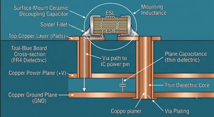
Plane Design, Decoupling Capacitors, and Via Placement
In tightly coupled power and ground planes, current flows between them in the high-MHz range with extremely low inductance, like a parallel-plate capacitor. The closer proximity between them, the more plane capacitance, and the less spreading inductance (both good for PDN impedance) for the same dielectric material between them. The mid-frequency bands are handled by decoupling capacitors, which are only as good as their mounting. Every capacitor carries:
- Its intrinsic series inductance (ISL) is caused by the package body
- Pad, Trace, and Via inductance losses due to mounting.
- Equivalent series resistance (ESR), which really assists in dampening anti-resonance peaks.
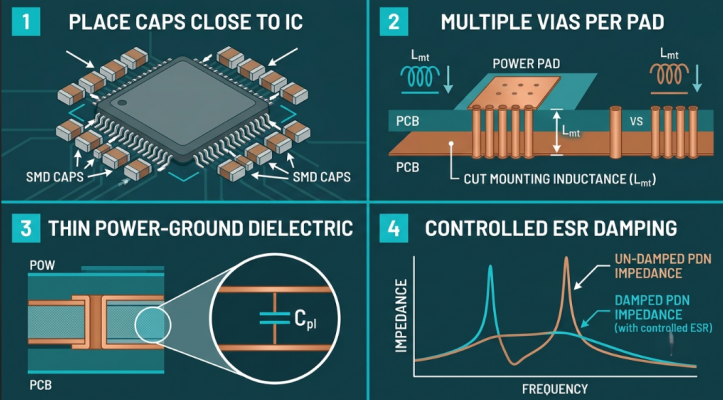
Typically, the mounting inductance dominates, and the effective high-frequency limit for the capacitor is determined by it. That is why it is more important to know the placement and via geometry rather than the printed capacitance value. My rules are practical, and here they are:
- Locate high-frequency ceramics near the IC power pins as close as possible.
- Use short, wide connections and put vias right at the capacitor pads, not on stubs.
- Reduce mounting inductance by using multiple vias per pad.
- Use a range of values to create a wide range, but be aware of the anti-resonances between them.
Material Selection and Layer Stackup Optimization
Plane capacitance is directly determined by the thickness and dielectric constant (Dk) of the material between the power and ground planes. The thin core between two power-ground layers is one of the best ways to decouple at high frequencies, and it doesn't cost you anything in component count! For most designs, standard FR4 with a Dk of 4.2 to 4.6 will do. Dedicated thin power-ground dielectrics or buried capacitance materials drive plane capacitance up for aggressive rails. The thickness of the layers in the stackup determines the distance between the planes, the thickness of the copper, and the length of the via paths. A good stackup will keep power and its return in close proximity, add decoupling planes close to the surface the IC resides on, and provide no unnecessary long and inductive detours for the return currents to take. In fact, stackup is not just a signal integrity decision; it's a power integrity decision as well.
Practical Techniques for PDN Impedance Analysis and Optimization
Simulation Tools and Measurement Methods
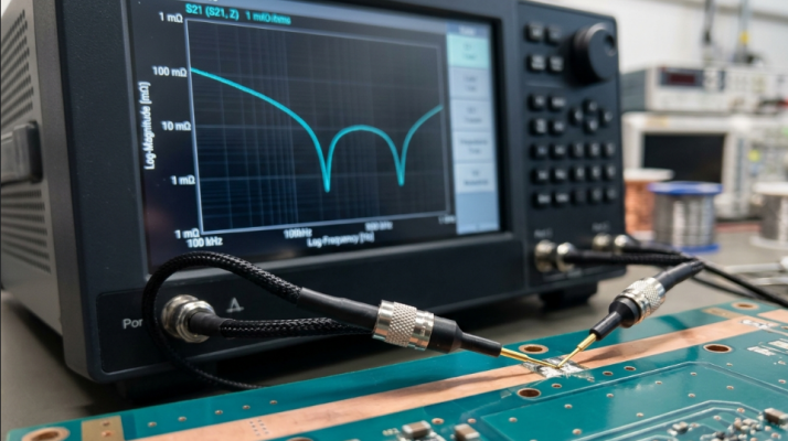
Pre-layout, frequency domain PDN tools allow you to draw the PDN impedance profile based on the VRM output impedance, capacitor models, plane capacitance, and on-die capacitance. Import the vendor's capacitor S-parameter models and view the curve before routing a single trace. Post-layout 3D field solvers and PDN extraction tools calculate the actual impedance with actual via positions, plane shapes, and mounting parasitics. This picks up the anti-resonance peaks, which idealized models do not catch.
A vector network analyzer (VNA) is used to perform a 2-port shunt-through measurement, which is the standard method for PDN impedance measurement on real hardware. It is a milliohm measurement, and a simple 1-port reflection measurement isn't quite fine enough. The shunt-through method is the method of choice that drives current through a rail on one port while sensing voltage is measured on a second port, allowing impedances to be resolved down into the sub-milliohm range. A semi-rigid coax or probe pair is placed directly on a clean rail-to-ground area near the load.
Reducing Impedance Peaks Through Design Adjustments
When you see a peak above target, you attack it purposefully, not blindly. My best moves:
- Look up the self-resonant frequencies of caps and fill in the gap with them.
- Slightly increase ESR or use controlled-ESR components to help suppress resonance.
- Minimize mounting inductance using improved via patterns & shorter connections.
- Reduce the thickness of the power-ground dielectric to increase the capacitance between the planes.
- Physically place capacitors closer to the load to change their effective range.
The idea is always to have a flat curve under the target line. Don't believe that more capacitors are better; a poorly placed bank can generate new anti-resonances. It is always better to use targeted fixes that are frequency aware than to use brute force.
Manufacturing Considerations for Low PDN Impedance
Copper Thickness, Plane Continuity, and Etching Precision
- Copper thickness directly sets the DC resistance and spreading inductance of your planes. A rail specified for 2 oz copper that ships at the low end of tolerance has measurably higher impedance, especially at DC and low frequency. Tight copper weight control matters.
- Plane continuity is just as important. Every slot, void, or unnecessary cutout in a power or ground plane forces return current to detour, adding inductance and raising impedance locally. Etching precision keeps plane edges clean and antipads consistent, so the copper you designed is the copper you actually get.
Process Controls to Maintain Designed Impedance in Production
It is important to maintain the thickness of the dielectric between the power and ground planes, as the capacitance of the planes is directly dependent on this. The 100µm core is not guaranteed to be 100µm all over the panel, depending on the lamination pressure, prepreg selected, and press cycle control. There are disciplined process controls that are essential to reliable low-impedance fabrication:
- Controlled lamination to maintain tight tolerances of the heights of the dielectrics.
- To realize a low inductance of via-to-plane connection, registration accuracy is crucial.
- Low resistance via barrels for power transfer through consistent plating.
JLCPCB's Expertise in PDN Impedance Optimized PCBs
Advanced DFM Review Focused on Power Delivery Networks
JLCPCB's design-for-manufacturing (DFM) review uncovers problems that silently affect PDN performance, such as thin plane connections, too many plane voids, too small power vias, and too far apart planes because of stackup choices. If you catch these before fabrication, then it saves a respin and won't mess up your impedance profile.
Their expertise in instant quoting and engineering feedback enables you to rapidly experiment with various stackups and copper weights, making power integrity decisions before an unsuccessful prototype. The speed, cost, and consistency are the factors that make this practical. TATs of 1 to 2 days, combined with $2 starting PCBs, allow for the prototyping of a power-critical board, real PDN measurement, iterations and refinement, and volume without switching vendors.
Precision Fabrication Ensuring Stable Impedance Performance
The fab needs to control copper weights, dielectric thicknesses, and registration very tightly to match the simulation for impedance. JLCPCB provides controlled-impedance manufacturing with precise stackups, multiple copper weights, and consistent lamination. All of which are important aspects of a PDN's ability to keep the plane capacitance and resistance on target. Multilayer builds with Blind and buried vias and a variety of materials allow placing power and ground planes as necessary in a power integrity strategy.
Conclusion
One of those areas is PDN impedance, which seems esoteric until a board fails under load, and you realize that things aren't as solid as the schematic would suggest. However, with the introduction of the concept of target impedance and a frequency profile, the entire problem becomes approachable. Design your planes and decoupling to remain below your Z_target, and confirm using the shunt-through VNA measurement on the output, trying to suppress anti-resonance peaks. What people don't realize is that all of this is based on faithful manufacturing. If a design is optimized to single-digit milliohms, the change in the thickness of the dielectric or the amount of copper used during production can destroy all the hard work. That's where combining a solid power integrity design with a precision manufacturer such as JLCPCB makes all the difference, and helps you move from a clean simulation to a board that keeps your rails quiet from the first prototype, through volume production.
FAQ about PDN Impedance
Q: What is PDN impedance in simple terms?
PDN impedance is the impedance that your power delivery network presents to a chip as a function of frequency. Keeping it low across the relevant band ensures the rail voltage stays stable when the chip suddenly demands current.
Q: How do I calculate PDN target impedance?
Use Z_target = (V_dd × allowed_ripple%) / I_transient. For a 1.0 V rail with a 5% budget and a 10 A transient, that is (1.0 × 0.05) / 10 = 5 mΩ, which your network must stay below across the band of interest.
Q: What causes anti-resonance peaks in a PDN?
Anti-resonance peaks occur when the inductance of one decoupling stage resonates with the capacitance of the next, creating a sharp impedance spike at a specific frequency. If a peak rises above your target impedance, a current step at that frequency produces excessive voltage noise.
Q: How is PDN impedance measured on a real board?
The standard method is a 2-port shunt-through measurement using a vector network analyzer (VNA). It drives current through the rail on one port and senses the resulting voltage on another, resolving the milliohm and sub-milliohm impedances that simple reflection methods cannot.
Q: Does PCB manufacturing affect PDN impedance?
Yes, significantly. Copper thickness, dielectric height between planes, plane continuity, and via plating all shift the real impedance away from simulation, so tight process control from your fabricator is essential to hold the designed values.
Conclusion
In high-performance PCB designs, flawless signal routing is not enough — stable power delivery is equally critical. Mastering PDN impedance helps eliminate voltage droop, reduce jitter, and ensure reliable operation under heavy transient loads.
By defining clear target impedance, optimizing stackup, plane capacitance, and decoupling strategies, you can maintain a flat, low-impedance power network. Remember that precise manufacturing — especially copper thickness, dielectric control, and via quality — is essential to turn simulation into reality.
With JLCPCB’s tight process control and reliable fabrication, you can achieve consistent PDN performance from prototype to production.
Popular Articles
Keep Learning
Optimizing Power Nets for Stable and Efficient High-Performance PCBs
Key Takeaways Power Nets as Systems: It is a complete copper network of planes, pours, traces, and vias built to deliver clean, stable voltage. Control IR Drop: Copper resistance causes voltage drop. Use wider traces, solid pours, or heavier copper (2 oz+) to stay within voltage tolerances. Minimize Loop Area: Place decoupling capacitors close to power pins with short, wide traces to handle fast transient currents. Scale Your Vias: A single 0.3mm via carries only 1 to 2A. High-current paths require pa......
Achieving Stable Power Delivery : Mastering PDN Impedance in High-Performance PCBs
Key Takeaways PDN impedance directly determines voltage stability under load. Keep it low and flat. Calculate your target: Z_target = (V_dd × Ripple%) / I_transient — typically single-digit milliohms. Prioritize close power-ground planes, short via connections, and strategic decoupling placement. Avoid anti-resonance peaks; a smooth curve matters more than raw capacitance. Precise manufacturing (copper thickness, dielectric control) is essential to match simulation results. There's no point in using a......
Phase Matching in High-Speed PCB Design: Achieving Signal Integrity with Precision Manufacturing
Key Takeaways Phase matching controls electrical trace length in high-speed PCBs to maintain precise signal timing and phase relationships. Even 10–15 ps skew (roughly 1–2 mm difference) at 10 Gbps can collapse eye diagrams, raise bit error rates, and cause system failures. Dynamic phase matching maintains alignment throughout the entire signal path, accounting for bends, vias, and layer transitions. USB 3.x SuperSpeed interfaces commonly target intra-pair skew below 5 mils (0.13 mm) to maintain relia......
Mastering Split Planes for Cleaner Power Delivery and Better Signal Integrity
Key Takeaways Split power planes when needed for multiple voltage domains or analog/digital isolation, but never split ground planes — always keep ground continuous for clean return paths. Avoid routing high-speed signals across splits; if unavoidable, use stitching capacitors (0.1 µF) and ensure differential pairs cross together. Place split power planes next to a solid ground layer, maintain ~10 mil moat width, and use proper decoupling near IC pins. Good split plane design significantly reduces noi......
Building Stable Power Delivery for High-Performance PCBs with Power Integrity Analysis
Key Takeaways Power integrity analysis is essential for building stable power delivery in high-performance PCBs. By maintaining low PDN impedance, optimizing decoupling capacitors, and designing robust power/ground planes with minimal voltage droop and inductance, engineers can prevent common failures such as voltage droop, ground bounce, and power-induced jitter. Combining thorough PI simulation with smart layout practices and professional manufacturing ensures reliable performance from prototype to ......
How Impedance Controlled Routing Delivers Reliable High-Speed PCB Performance
Key Takeaways Impedance Controlled Routing is essential for reliable high-speed PCB performance above 1 Gbps, eliminating reflections, ringing, and bit errors by precisely targeting interface-specific impedances (USB 90 Ω, PCIe 85 Ω, DDR4 40/80 Ω, HDMI 100 Ω) through field-solver calculations, symmetrical stackups with continuous reference planes, stable low-loss dielectrics, and strict single-ended/differential routing rules. Manufacturing precision in etching, copper profile, and lamination, verifie......