
Phase Matching in High-Speed PCB Design: Achieving Signal Integrity with Precision Manufacturing
12 min
- What is Phase Matching in PCBs and Why It Matters
- Fundamental Principles Behind Phase Matching
- Design Best Practices for Effective Phase Matching
- Manufacturing Challenges and Solutions for Precise Phase Matching
- Common Pitfalls in Phase Matching and How to Avoid Them
- Partnering with Experts for Reliable Phase-Matched PCBs
- FAQ about Phase Matching in High-Speed PCB Design
Key Takeaways
- Phase matching controls electrical trace length in high-speed PCBs to maintain precise signal timing and phase relationships.
- Even 10–15 ps skew (roughly 1–2 mm difference) at 10 Gbps can collapse eye diagrams, raise bit error rates, and cause system failures.
- Dynamic phase matching maintains alignment throughout the entire signal path, accounting for bends, vias, and layer transitions.
- USB 3.x SuperSpeed interfaces commonly target intra-pair skew below 5 mils (0.13 mm) to maintain reliable links.
- Material selection, impedance control, and manufacturing precision must work together for consistent phase performance.
- JLCPCB supports phase-matched designs with documented material properties, a free impedance calculator, DFM reviews, and TDR verification.
Phase matching stands as one of the cornerstone requirements in high-speed PCB design today. With data rates climbing into multi-gigabit and millimeter-wave ranges, even minor differences in propagation delay—commonly called skew—can collapse eye diagrams, raise bit error rates, and trigger complete system failures.
Phase matching ensures signals, especially in differential pairs, arrive at their destinations with the intended timing and phase relationships. Achieving this demands tight coordination between electrical design, simulation, material selection, and manufacturing precision. Manufacturers like JLCPCB support designers with documented material properties, advanced lamination, tight process controls, and verification tools such as TDR testing.
What is Phase Matching in PCBs and Why It Matters
Phase matching means deliberately controlling the electrical length of traces so that related signals experience equal—or intentionally offset—propagation delays. In differential signaling, the goal is to preserve a near-perfect 180-degree phase relationship between the positive and negative traces while minimizing intra-pair skew. For clock distribution, address buses, or parallel interfaces, it reduces inter-signal timing differences that could violate setup and hold times.
Static vs. Dynamic Phase Matching Explained
Static phase matching focuses on equalizing the total end-to-end electrical length. Designers typically achieve this through length-tuning structures such as serpentines. It works well for simpler designs but often falls short in complex multilayer boards.
Dynamic phase matching, by contrast, maintains alignment not just at the endpoints but throughout the entire signal path. This approach accounts for bends, vias, layer transitions, and plane splits. When one trace in a differential pair takes a detour, the companion trace receives symmetric compensation to avoid introducing localized phase disturbances. At speeds above a few Gbps, dynamic considerations frequently become the dominant factor because short sections of mismatch can generate reflections or unwanted differential-to-common-mode conversion.
The Impact of Phase Skew on Signal Integrity
Phase skew produces several measurable problems:
- Conversion of differential signals into common-mode noise, increasing EMI emissions and susceptibility.
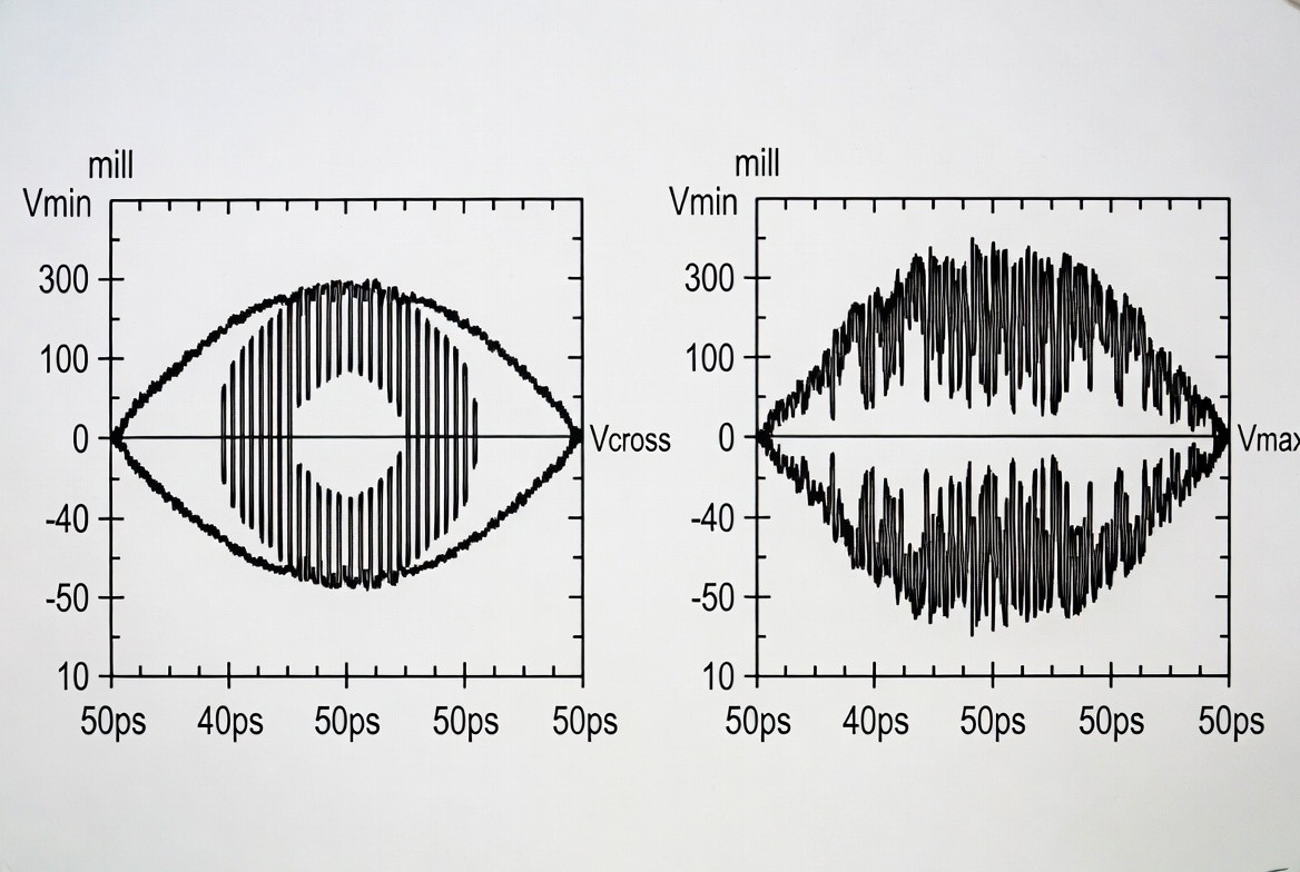
- Horizontal closure of eye diagrams, directly reducing timing margins.
- Elevated bit error rates (BER) in serial links.
- Degraded performance in RF systems, such as inaccurate beam steering in phased arrays or poor image rejection in mixers.
At 10 Gbps, a skew of only 10–15 ps (roughly 1–2 mm length difference in standard FR-4) can noticeably degrade performance. USB 3.x SuperSpeed interfaces commonly target intra-pair skew below 5 mils to maintain reliable links.
Key Applications: High-Speed Digital, RF, and Microwave Circuits
Phase matching finds use across many domains:
- High-speed digital interfaces — PCIe Gen4/Gen5, USB4, DDR5, 25G/56G Ethernet, where tight matching preserves setup/hold timing.
- RF and microwave systems — 5G front-ends, radar modules, and satellite communications that require phase coherence across channels.
- Mixed-signal designs — High-speed ADCs and DACs that need matched clock and data paths for accurate sampling.
In all cases, phase matching works hand-in-hand with impedance control and crosstalk management.
Fundamental Principles Behind Phase Matching
Propagation Delay and Trace Length Matching
Propagation delay depends primarily on the effective dielectric constant (Dk) and the physical geometry of the trace. In typical FR-4 materials, signal velocity approximates $1/\sqrt{Dk}$ of the speed of light in vacuum, resulting in roughly 150–170 ps per inch for microstrip configurations. Designers calculate the necessary length compensation according to the specific stackup and then validate it through simulation. Even minor variations in Dk or copper surface roughness can shift actual delay, which is why access to manufacturer-provided material data becomes invaluable for accurate predictions.
Differential Pairs and 180-Degree Phase Requirements
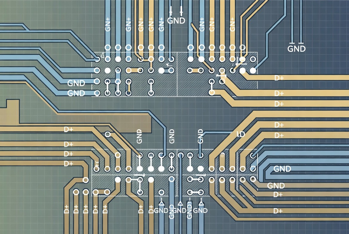
Differential pairs transmit complementary signals that ideally cancel noise and EMI when properly balanced. Maintaining the 180-degree relationship requires extremely tight intra-pair length matching. For USB 3.0 SuperSpeed links, industry practice commonly limits intra-pair mismatch to approximately 5 mils (0.13 mm). Routing must keep spacing uniform and traces parallel over continuous reference planes to preserve the target differential impedance—often 90 Ω for USB or 85–100 Ω for PCIe. Any asymmetry, such as one trace encountering additional vias, quickly disrupts this balance and introduces common-mode noise.
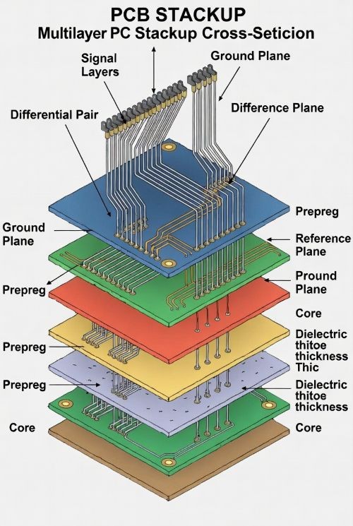
Factors Affecting Phase: Dielectric Constant, Trace Geometry, and Fiber Weave Effect
Several variables influence phase performance:
- Dielectric Constant (Dk): Variations within a panel or between layers directly create skew.
- Trace Geometry: Width, spacing, height to reference plane, and copper thickness all affect propagation velocity.
- Copper Roughness: Adds both loss and minor delay.
- Fiber Weave Effect: The glass-resin structure in FR-4 produces periodic delay variations; routing at 45° angles or choosing tighter weave prepregs helps mitigate this.
| Prepreg Type | Dielectric Constant (Dk) | Common Use Case | Notes |
|---|---|---|---|
| 7628 | 4.4 | Standard multilayer cores/prepregs | Higher resin content options available |
| 3313 | 4.1 | Tighter impedance control | Lower Dk for reduced delay |
| 1080 | 3.91 | Fine-line high-speed layers | Good for lower loss |
| 2116 | 4.16 | Balanced multilayer stackups | Versatile mechanical properties |
Design Best Practices for Effective Phase Matching
Length Tuning Techniques: Serpentine vs. Other Methods
Serpentine tuning remains popular because of its simplicity, yet it requires careful implementation. Individual tuning segments should stay relatively short, with sufficient spacing between folds to limit unwanted coupling. Apply identical tuning patterns symmetrically to both legs of the differential pair. Positioning the tuning section near the origin of the skew, rather than at the far end of a long route, often yields better results. In space-constrained areas, trombone or alternative delay-line structures sometimes perform more effectively. Advanced practitioners always simulate the tuned geometry in a 3D field solver to evaluate any introduced reflections or impedance disturbances. The overarching objective is accurate delay compensation without compromising overall signal quality.
Impedance Control Integration with Phase Matching
Phase matching and impedance control cannot be treated separately. Length-tuning structures that change trace geometry risk altering local impedance unless carefully managed. JLCPCB provides a free online impedance calculator that incorporates specific stackup parameters, prepreg types, and solder mask effects. Designers commonly target 90 Ω differential for USB or 100 Ω for other high-speed interfaces. When controlled impedance is specified, the manufacturer aims for ±10% tolerance using defined processes. Selecting an appropriate stackup variant ensures both impedance targets and phase consistency remain achievable within practical manufacturing limits.
Simulation and Verification Tools for Phase Analysis
A robust verification strategy spans multiple stages. Pre-layout tools such as HyperLynx, ADS, or Ansys HFSS optimize routing rules and stackups. Post-layout extraction incorporates realistic via and connector models for time-domain eye diagram and S-parameter analysis that includes material variations. On the manufacturing side, Time Domain Reflectometry (TDR) testing on coupons helps correlate simulation predictions with actual fabricated boards. This layered approach progressively builds confidence that the final product will meet design targets.
Manufacturing Challenges and Solutions for Precise Phase Matching
Material Selection and Dielectric Consistency for Low Skew
Material selection establishes the foundation for phase stability. Standard FR-4 exhibits some Dk variation, making the choice of prepregs with published values important for risk reduction. In more demanding applications, low-loss laminates deliver improved phase performance across frequency and temperature ranges. JLCPCB offers multiple prepreg options with consistent resin content and glass styles, helping to minimize the fiber weave effect that could otherwise introduce localized delay differences.
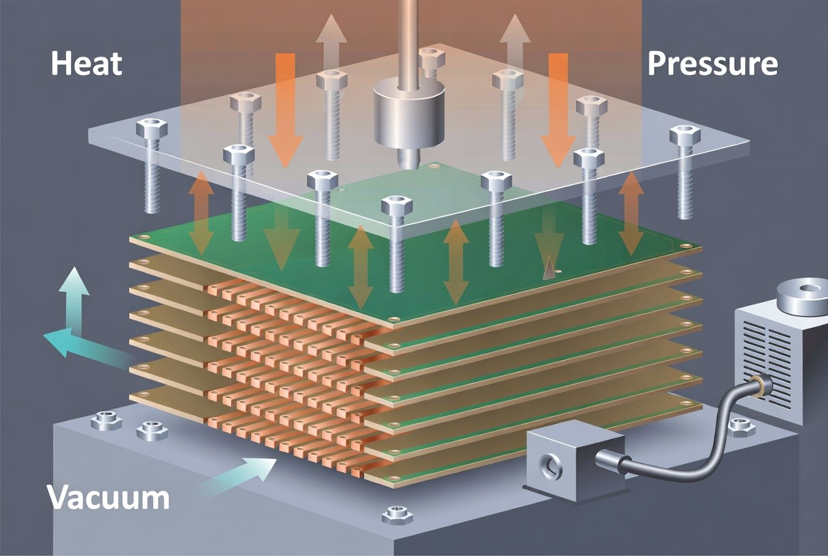
Advanced Lamination and Etching Processes for Tight Tolerances
Vacuum-assisted lamination applies uniform pressure and temperature across the panel. This reduces dielectric thickness variation and helps eliminate voids or resin-rich pockets. Precision etching controls trace width and edge profile—both critical because even small deviations affect impedance and electrical length. Tight layer-to-layer registration ensures traces remain properly aligned relative to their reference planes. JLCPCB supports minimum trace width and spacing down to 3.5 mil together with multilayer processes optimized for these precision requirements.
Common Pitfalls in Phase Matching and How to Avoid Them
Via Effects and Compensation Techniques
Vias introduce discontinuities, stub inductance, and extra delay that can unbalance differential pairs. In designs running above 10 Gbps, back-drilling effectively removes unused stubs. Placing ground return vias close to signal vias helps maintain current return paths. Simulating via transitions in 3D field solvers allows designers to quantify effects and apply compensation methods such as optimized anti-pads when needed. The most straightforward mitigation remains minimizing unnecessary layer changes for critical matched nets.
Bend and Routing Asymmetries
Sharp bends or unequal routing conditions create both phase and impedance imbalances. Mitered or rounded bends help reduce these effects. Both legs of a differential pair should experience nearly identical routing conditions, including identical tuning patterns. Avoiding situations where one trace crosses a plane split that the other does not encounter preserves symmetry. Maintaining the same layer and reference structure for matched pairs provides the most reliable prevention.
Tolerance Stack-Up in High-Volume Production
Cumulative variations from etching, lamination thickness, material Dk tolerance, and registration can exceed design budgets during volume manufacturing. Early DFM engagement, clear specification of critical nets and impedance requirements, and selection of a manufacturer with strong process controls and test data all help reduce this risk significantly.
Partnering with Experts for Reliable Phase-Matched PCBs
Getting Started with Phase Matching Projects Today
- Start by comparing your intended stackup against JLCPCB's published options and using their impedance calculator to determine appropriate trace geometries.
- Select controlled impedance where critical and clearly annotate phase-matched nets in fabrication notes.
- Upload designs early for DFM feedback to allow potential issues to surface before production.
- With thoughtful planning and a capable manufacturing partner, robust phase matching becomes a repeatable process that shortens development cycles and improves overall product reliability.
FAQ about Phase Matching in High-Speed PCB Design
Q: What is phase matching in PCB design?
Phase matching is the deliberate control of electrical trace length so that related signals experience equal or intentionally offset propagation delays. In differential signaling, the goal is to preserve a near-perfect 180-degree phase relationship while minimizing intra-pair skew.
Q: Why is phase matching important for high-speed signals?
At multi-gigabit data rates, even minor skew can collapse eye diagrams, raise bit error rates, and trigger complete system failures. At 10 Gbps, a skew of only 10–15 ps (roughly 1–2 mm difference in standard FR-4) can noticeably degrade performance.
Q: What is the difference between static and dynamic phase matching?
Static phase matching equalizes total end-to-end electrical length using techniques like serpentines. Dynamic phase matching maintains alignment throughout the entire signal path, accounting for bends, vias, layer transitions, and plane splits, which becomes critical at speeds above a few Gbps.
Q: How much intra-pair skew is acceptable for high-speed interfaces?
For USB 3.0 SuperSpeed links, industry practice commonly limits intra-pair mismatch to approximately 5 mils (0.13 mm). Different interfaces have specific requirements, and always consult the relevant standard for exact limits.
Q: What factors affect phase performance in PCBs?
Key factors include dielectric constant (Dk) variations, trace geometry (width, spacing, height), copper surface roughness, and the fiber weave effect in FR-4 materials. All of these influence propagation velocity and must be accounted for during design.
Q: How does the fiber weave effect impact phase matching?
The glass-resin structure in FR-4 produces periodic delay variations because signals travel at different speeds through glass bundles versus resin-rich areas. Routing at 45° angles or choosing tighter weave prepregs helps mitigate this effect.
Q: How does JLCPCB support phase-matched PCB manufacturing?
JLCPCB provides documented material properties, a free online impedance calculator, advanced lamination with tight process controls, DFM reviews, and TDR verification services to help transform simulations into reliable phase-matched production boards.
Conclusion on Phase Matching in High-Speed PCB Design
Mastering phase matching is essential for achieving reliable signal integrity in high-speed PCB designs. It requires close attention to trace length control, impedance matching, material consistency, and precise manufacturing processes to minimize skew and maintain timing accuracy.
By combining sound design practices with professional fabrication support, engineers can reduce respins, shorten development cycles, and deliver robust systems with excellent signal integrity.
Popular Articles
Keep Learning
How to Choose and Place Decoupling Capacitors for PCB Design
Every digital PCB depends on decoupling capacitors, yet a surprising number of boards still suffer from voltage dips, glitches, and electromagnetic interference (EMI) issues caused by one simple mistake: incorrect placement or selection. This guide walks through what decoupling capacitors do, how to choose the right value, where to place them, and which layout mistakes to avoid, so your next board runs clean on the first try. Key Takeaways Place one decoupling capacitor near each IC's power pin. Use 1......
Understanding DC 5V Input in PCB Design: Key Considerations
Note Correct Input: Power 5V through USB or header pins, as barrel jacks require at least 6.5V. Trace Sizing: Use 1.3mm traces on 1oz copper for 2A loads to keep voltage within 5%. Regulator Choice: Use LDOs for low-current analog circuits and Buck regulators for loads over 1A. Thermal Design: Place 0.3mm drill thermal vias on a 1.0mm grid under power ICs. Input Protection: Safeguard 5V inputs with a 5.6V TVS diode and a PPTC resettable fuse. DC 5V input is a critical aspect of PCB design, ensuring vo......
Optimizing Power Nets for Stable and Efficient High-Performance PCBs
Key Takeaways Power Nets as Systems: It is a complete copper network of planes, pours, traces, and vias built to deliver clean, stable voltage. Control IR Drop: Copper resistance causes voltage drop. Use wider traces, solid pours, or heavier copper (2 oz+) to stay within voltage tolerances. Minimize Loop Area: Place decoupling capacitors close to power pins with short, wide traces to handle fast transient currents. Scale Your Vias: A single 0.3mm via carries only 1 to 2A. High-current paths require pa......
Achieving Stable Power Delivery : Mastering PDN Impedance in High-Performance PCBs
Key Takeaways PDN impedance directly determines voltage stability under load. Keep it low and flat. Calculate your target: Z_target = (V_dd × Ripple%) / I_transient — typically single-digit milliohms. Prioritize close power-ground planes, short via connections, and strategic decoupling placement. Avoid anti-resonance peaks; a smooth curve matters more than raw capacitance. Precise manufacturing (copper thickness, dielectric control) is essential to match simulation results. There's no point in using a......
Phase Matching in High-Speed PCB Design: Achieving Signal Integrity with Precision Manufacturing
Key Takeaways Phase matching controls electrical trace length in high-speed PCBs to maintain precise signal timing and phase relationships. Even 10–15 ps skew (roughly 1–2 mm difference) at 10 Gbps can collapse eye diagrams, raise bit error rates, and cause system failures. Dynamic phase matching maintains alignment throughout the entire signal path, accounting for bends, vias, and layer transitions. USB 3.x SuperSpeed interfaces commonly target intra-pair skew below 5 mils (0.13 mm) to maintain relia......
Mastering Split Planes for Cleaner Power Delivery and Better Signal Integrity
Key Takeaways Split power planes when needed for multiple voltage domains or analog/digital isolation, but never split ground planes — always keep ground continuous for clean return paths. Avoid routing high-speed signals across splits; if unavoidable, use stitching capacitors (0.1 µF) and ensure differential pairs cross together. Place split power planes next to a solid ground layer, maintain ~10 mil moat width, and use proper decoupling near IC pins. Good split plane design significantly reduces noi......