Optimizing Power Nets for Stable and Efficient High-Performance PCBs
13 min
- Understanding Power Nets in PCB Design
- Why Power Net Management Matters in Modern Designs
- Core Principles of Effective Power Net Design
- Advanced Techniques for Power Net Optimization
- Manufacturing Considerations for Robust Power Nets
- JLCPCB's Expertise in Power Net Optimized PCBs
- FAQ about PCB Power Net
- Conclusion
Key Takeaways
- Power Nets as Systems: It is a complete copper network of planes, pours, traces, and vias built to deliver clean, stable voltage.
- Control IR Drop: Copper resistance causes voltage drop. Use wider traces, solid pours, or heavier copper (2 oz+) to stay within voltage tolerances.
- Minimize Loop Area: Place decoupling capacitors close to power pins with short, wide traces to handle fast transient currents.
- Scale Your Vias: A single 0.3mm via carries only 1 to 2A. High-current paths require parallel arrays of multiple stitched vias.
- DFM Matters: Ensure your design matches physical reality by verifying copper thickness, etching, and stackup with a reliable fabricator.
Once, a board that I had browned out under load, I thought it was the cause of everything, but it wasn't. I tested the regulator, replaced the capacitors, and even asked my bench power supply. It was a skinny 0.3mm trace on half the board, running 5V power down to the load, that was the problem, which meant a loss of almost 200mV en route. That was a lesson that I never forgot. The power net is more than just "the wire that carries voltage"; it is the whole copper structure of planes, pours, traces, and vias that are used to deliver a power rail to all the components that require it.
If you don't take it seriously, you have voltage droop and noise, and the type of failures that are most annoying to troubleshoot. In this article, I would like to discuss the power nets I think about today: what they are, why they are more important than ever in a dense multi-voltage design, fundamental design rules, advanced optimization, and manufacturing considerations that determine whether your pretty power net will actually function in production. Let's get into it.
Understanding Power Nets in PCB Design
What Power Nets Are and Their Fundamental Role
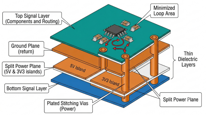
A power net is the copper that carries one power rail (such as 3V3, 5V, or VCORE) from its source to all loads that use it. It may be in the form of a dedicated plane, a polygon pour, a wide trace, or most commonly a combination of all three stitched together with vias. The primary duty of a power net is very easy: Supply a clean and stable voltage to all the loads at all times, no matter how much current is flowing. That is, carry out continuous DC current without overheating and provide rapid transient current without dropping the voltage. Imagine that it's plumbing in a building. A signal net is a thin tube that conveys a message; a power net is the main water supply that supplies all faucets simultaneously. If the pipe is too small or the pressure goes down, all points downstream are adversely affected.
Difference Between Power Nets and Signal Nets
The power net and the signal net are different kinds of animals, and it's a beginning mistake to think they're the same. I divide them up like this:
- Current: Milliamps on signal nets; amps or tens of amps on power nets.
- Geometry: Signals prefer narrow traces, power nets prefer wide pours, and planes with low resistance.
- Failure mode: A bad signal net causes data errors, and a bad power net causes a drop in voltage, heat, and total shutdown.
- Reference: Signals require a continuous return path; Power nets require a low-impedance partner ground plane.
| Property | Signal Net | Power Net |
|---|---|---|
| Typical current | µA to mA | mA to tens of A |
| Preferred copper | Narrow trace | Plane / wide pour |
| Key concern | Impedance, timing | IR drop, current capacity |
| Optimization goal | Signal integrity | Power integrity |
Why Power Net Management Matters in Modern Designs
Impact on Voltage Drop, Noise, and System Stability
The one most critical equation of power net design is Ohm's law for Copper: V = I × R. Each milliohm of resistance in your power net produces a voltage drop, and that drop is the IR drop. As an example, let's take a 10A rail and have only 5mΩ of resistance in a power net. This corresponds to a drop of 50mV. Even a core rail rated as 0.9V with a 3% tolerance window of just 27mV is already beyond your budget without even taking into account transients or noise.
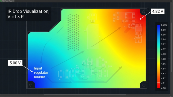
Except for static IR drop, switching loads introduce noise. Sloppy power nets allow that noise to propagate throughout, where it can couple into sensitive analog and high-speed portions. In good power net management, the rail keeps stiff, quiet, and stable throughout its entire operating range.
Challenges in High-Current and Multi-Voltage Designs
Today's boards routinely contain a dozen or more rails: 12vin, 5V, 3V3, 1V8, 1V2, 0V9 core, etc. Each one is a power net which is independent of the others and is fighting for the plane area and via space in the stackup.
- Plane scarcity: It is rare to have enough layers to allocate each rail to its unique solid plane, and so layers become split planes or islands.
- High transient currents: GaN converters and new SoCs require high transient currents that traditional nets just can't provide cleanly.
- Thermal coupling: Hot nets with high currents affect nearby component behavior.
- Return-path conflicts: Split power planes can disrupt return paths of signals that are routed above them.
Core Principles of Effective Power Net Design
Plane Allocation, Current Carrying Capacity, and IR Drop Control
The first big decision you have to make is related to plane allocation. In a 4-layer board, typically I use one of the internal layers as ground and divide the second internal layer into several current/power layers depending on the sensitivity and current flow of the signals, with the least sensitive, highest current layer needing the heaviest copper. Copper cross-section determines Current Carrying Capacity, and the industry standard reference is IPC-2152. The width of the trace and the thickness of copper (in ounces per square foot, 1 oz copper is about 35 µm, 2 oz is about 70 µm) determine the cross-section.
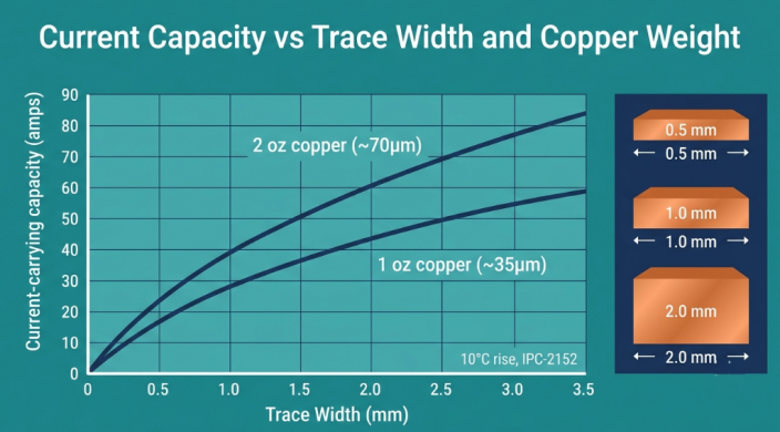
A simple guideline for external 1 oz copper is that a 1mm-wide trace will be able to safely carry 2-3A for a modest temperature increase of 10°C. Need more current? You increase the copper, pour a plane, or go up to a 2 oz copper to double the cross-section without increasing board area.
Decoupling Strategy and Loop Area Minimization
DC can be handled by static copper; fast transients require local energy reservoirs. That's what decoupling capacitors are for, and all they can do is rely, almost entirely, on their layout. The bad guy is area, known as loop inductance, and defined as the space through which current flows from the cap, power net to the load, then back through ground. Each nanohenry of loop inductance opposes the cap during rapid changes in current.
- Small (1 to 100nF), high-frequency capacitors near the power pins.
- Avoid long, thin connections from pad to via and via straight down to the plane.
- Keep the power plane and its adjacent ground plane separation (dielectric) to a minimum to reduce the vertical loop.
- For low-frequency bulk demand, add bulk capacitance (10-100µF) further out.
Advanced Techniques for Power Net Optimization
Simulation, Analysis Tools, and Target Impedance Planning
The Power Distribution Network (PDN) and its target impedance are the bridge between static power nets and dynamic behavior. Target impedance is the highest impedance that the rail can present while maintaining voltage tolerance, under the worst-case transient current. The classic formula is Z_target = ΔV / ΔI, where ΔV is the voltage ripple you can tolerate, and ΔI is the transient current step. If a 1V rail has 2% tolerance and is subject to a 5A transient, the desired result is 0.02V / 5A, or 4mΩ in the frequency range of interest. This is where modern EDA tools pay their way. DC IR-drop solvers display a color map of voltages across the plane, and AC PDN analyzers ensure that your power net plus decoupling remains below target impedance from DC to hundreds of MHz. There's no point in going for droop on the bench when you can simulate first before trying to fabricate.
Layout Best Practices for Complex Power Distribution
If the rails are multiplied, the power nets remain clean due to the layout discipline:
- For high current rails, pour the copper; do not route because a solid polygon pour reduces the overall impedance over thin traces.
- Vias should be stitched out liberally; vias have a limited current capacity, and multiple vias should be used in parallel to perform a plane-to-plane transition.
- Avoid dismembering planes, use planes continuously, and do not slice them with traces or unnecessary cutouts.
- Place sources and loads in close proximity to each other to shorten the net and reduce IR drop.
A quick via note: a typical 0.3mm plated via will carry 1-2A comfortably, thus a 10A transition will require a small array, not a single via. A habit to get into is to treat the vias as current-rated components, and not just connections.
Manufacturing Considerations for Robust Power Nets
Copper Thickness, Plane Continuity, and Etching Uniformity
The copper weight is a nominal target; the actual thickness will depend on the plating/etching. Designing for an IR drop budget based on 2 oz copper only to find that you are getting thin copper or uneven copper increases the actual resistance and reduces your margins.
- The resistance of your power net is determined by the thickness and consistency of the copper.
- Uniformity of etching is important because over-etching narrows pours and undercutting edges results in a smaller cross-section.
- Plane continuity needs to survive lamination, voids, or misregistration that disrupts the low-impedance plane you've created.
Designing for heavy current can mean the difference between a board that runs cool and a board that browns out, and specifying and verifying heavy copper (2 oz and above) can make all the difference.
Process Control to Ensure Designed Performance in Production
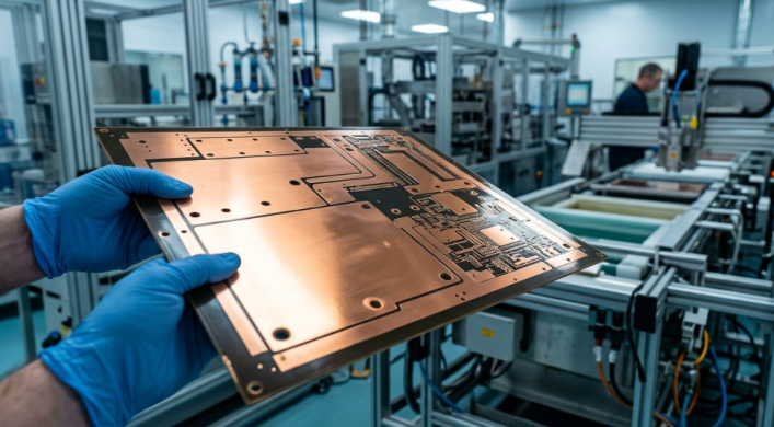
When moving from prototype to thousands of units, repeatability is key. If a power net, which is fine on board 1 but crazy on board 500, is a robust design, it is the luckiest one around. The thickness of copper plating, etch compensation, lamination pressure, and layer registration are all controlled tightly. And it makes sure that the power net that is actually manufactured can match the simulated one. Asymmetrical stackups are also important here, as asymmetry and lamination heat lead to warpage that stresses copper and joints. This is where a competent fabricator can come in handy.
JLCPCB's Expertise in Power Net Optimized PCBs
Creating a great power net is half the job; the other half is getting a manufacturer to reproduce it. This is the one thing that JLCPCB has always done for my boards.
Professional DFM Review Focused on Power Distribution
The automated verification of DFM in JLCPCB identifies the problems that silently destroy power nets, such as the inadequate copper thickness for the expected current, a marginal number of vias, plane discontinuities, etc. These will be caught before fabrication, thus saving a respin and a lot of bench debugging.
JLCPCB maintains plane continuity and copper thickness close to design intention with controlled copper weight (even heavy copper), tight etching tolerance, and well-managed multilayer lamination. That consistency is what will allow your IR-drop and target-impedance budgets to be true on the real board. The same process control is used from the prototype with a price tag of $2 to full-scale production runs. So if a power net passes the simulation, it is the same for unit 1 and unit 10000. Fast turnaround, instant quoting, and in-built SMT assembly allow you to iterate quickly without compromising on power integrity.
FAQ about PCB Power Net
Q: What exactly is a power net in PCB design?
A power net is the entire copper network from planes, polygon pours, and traces to vias that distributes one supply rail, such as 3V3 or 5V, from its source to every load that consumes it. Unlike a signal net, its job is to deliver clean, stable voltage at high current rather than carrying information.
Q: How does the IR drop affect my power net?
IR drop is the voltage lost to resistance, following V = I × R, where I is the load current and R is the resistance of your copper. Even a few milliohms across a high-current net can drop tens of millivolts, which can exceed the tight tolerance of low-voltage core rails. You reduce it with wider copper, planes, shorter paths, and more parallel vias.
Q: What copper weight should I use for high-current power nets?
It depends on your current and acceptable temperature rise, with IPC-2152 as the reference. As a rough guide, 1 oz copper (~35µm) handles light rails, while 2 oz copper (~70µm) doubles the cross-section for high-current rails without consuming extra board area. For heavy power delivery, heavy copper of 2 oz and above is common.
Q: Why does decoupling capacitor placement matter so much?
Decoupling effectiveness depends on loop inductance, which is set by the area of the current path from the cap through the power net and back through ground. Placing high-frequency caps right at the power pins with short, fat connections and nearby vias minimizes that loop, letting the cap actually supply fast transients. Poor placement makes even a good capacitor nearly useless.
Conclusion
A power net is much more than "VCC" on your schematic. It's a current delivery system, just like any other system; it should be designed to have enough copper to carry the current, have a small enough resistance to limit IR drop, have tight decoupling for transients, and have a stackup that's designed to keep the impedance below the target value over frequency.
Power net management is going to be more important as rails proliferate and transient currents increase. Once the copper, the planes, and the loop areas are correct, team up with a fabricator, such as JLCPCB, who can duplicate that design with tight control of copper, planes, and your board will keep things cool, quiet, and stable under load. Treat your power nets like first-class citizens, and they'll do their job quietly for you, which means that you won't be debugging a mysterious brownout ever again.

Popular Articles
Keep Learning
Navigating the Impedance Landscape: Selecting the Right Impedance for USB, Ethernet, HDMI, and SD Card Interfaces
Introduction In the realm of high-speed digital communication, choosing the right impedance is a critical aspect of successful PCB design. Impedance matching ensures optimal signal integrity, minimizes reflections, and enhances the overall performance of interfaces such as USB, Ethernet, HDMI, and SD Card. In this blog post, we'll explore the importance of impedance, the factors influencing impedance selection, and best practices for ensuring reliable data transmission in these widely used interfaces.......
A Beginners Guide to Impedance Control in PCBs
When a digital signal is transmitted from one point to another, it causes a change in the state of the signal line. This change can be understood as an electromagnetic wave moving through the circuit. Reflection occurs when this wave encounters a boundary between different mediums. At this boundary, some of the wave's energy continues as a signal, while the rest is reflected. This process repeats until the energy is either absorbed by the circuit or dissipated into the environment. For electrical engi......
What is PCB Signal Attenuation: How Signals Weaken Over Distance and How to Mitigate It
Key Takeaways Primary Causes: Signal attenuation is mainly caused by skin effect (conductor loss) and substrate energy absorption (dielectric loss). How to Mitigate: Reduce loss by using wider traces, low-loss materials, controlled impedance, and removing via stubs. JLCPCB Solutions: JLCPCB offers Rogers high-frequency laminates, High-TG FR4, precision impedance control, and backdrilling to protect signal integrity. As a signal travels from the source to the load through PCB conductors, the signal is ......
Understanding Analog and Digital Ground in PCB Design
When working on printed circuit board (PCB) design, proper grounding is crucial for ensuring signal integrity, minimizing noise, and maintaining reliable performance. Two common types of ground planes used in PCB layouts are Analog and Digital ground. In this article, we will explore the differences between analog and digital ground, their significance in PCB design, and best practices for their implementation. Analog Ground vs. Digital Ground Analog ground and digital ground have separate purposes in......
Design Guide for USB-3.0 Differential Signaling
In the world of data transfer, USB 3.0 is the Usain Bolt to USB 2.0’s friendly jogger. USB 2.0 is called “High Speed” and limped along at 480 Mb/s, whereas USB 3.0 SuperSpeed rockets up to 5 Gb/s (over ten times faster). But this speed jump brings full‑duplex operation and new differential transmit (SSTX) and receive (SSRX) pairs on dedicated pins. USB 2.0 D+/D– lines handle enumeration and legacy data, while two new 5 Gb/s high‑speed differential pairs carry SuperSpeed data in each direction. While m......
Understanding Impedance Matching for High-Speed PCB Designs
With the advancement of technology and the ever wider application of integrated circuits, the frequency and speed of electronic signal transmission have been increasing, making it essential for PCB conductors to provide high-performance transmission lines. These transmission lines are responsible for delivering signals from a source to the input of a receiver accurately and completely. This requirement emphasizes the need for impedance matching. Electrical impedance, commonly represented as Z and meas......