Fast Turn Flex PCB: Rapid Prototyping & Lead Time Guide
17 min
- What Is a Fast Turn Flex PCB?
- Why Choose Quick Turn Flex PCB for Rapid Product Development?
- How are fast-turn flex PCBs manufactured?
- Key Factors Affecting Fast Turn Flex PCB Lead Time
- How to Prepare Your Flex PCB Design for Faster Production?
- Fast Turn Flex PCB Panelization and SMT Assembly Considerations
- Choosing a Fast Flex PCB Manufacturer
- JLCPCB's Fast Turn Flex PCB Manufacturing Capabilities
- Conclusion
- Frequently Asked Questions About Fast Turn Flex PCB
Fast turn flex PCB service is what stands between a validated concept and a product that ships this quarter. Most flex delays are not caused by the factory. They come from a coverlay opening drawn 0.05 mm too tight or a missing stiffener drawing, and each one parks your job while an engineer emails.
In this guide, you will learn:
- What separates fast-turn flex PCB from standard FPC production
- Which design choices add days to the flex PCB lead time
- Panel, fiducial, and carrier rules for flex SMT assembly
- How to prepare files so the engineering review does not stall
What Is a Fast Turn Flex PCB?
Definition of Fast Turn Flex PCB
A fast-turn flex PCB is a flexible printed circuit built on a compressed schedule, typically four to five days rather than the three to six weeks a conventional custom FPC order takes. Speed comes from a constrained menu of stocked materials, automated design review, and digital imaging that skips physical tooling. It is not a faster factory; it is an express lane, and an express lane only works if everyone in it has exact change.
How Fast Turn Flex PCB Differs from Standard Flex PCB Production
Quick-turn flex circuits run a different path, not a rush fee on the same one, and every shortcut is paid for by giving up an option somewhere else.
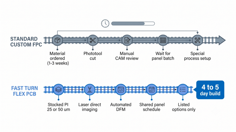
- Material sourcing. Standard jobs order laminate per job, often 1 to 3 weeks. Fast turn uses stocked 25 µm (1 mil) and 50 µm (2 mil) polyimide only.
- Imaging. Laser direct imaging writes straight from Gerber data: no phototool, no tooling wait.
- Design review. Automated DFM against a published capability set returns feedback in minutes.
- Panel loading. A shared panel on a fixed release schedule lets five pieces build on their own.
- Special processes. The menu shrinks to listed stiffener thicknesses and ENIG.
When to Choose Fast Turn Flex PCB for Your Project
Fast turn suits the first three or four builds, while you are still discovering whether the flex fits the enclosure: mechanical fit checks, connector and stiffener validation, bring-up boards for firmware teams, and runs of 5 to 200 pieces where tooling never amortizes. It is the wrong tool for Class 3 medical and aerospace builds needing qualification data, for liquid crystal polymer or rigid-flex constructions that need engineering conversation, and for any design depending on a material outside the stocked list.
Why Choose Quick Turn Flex PCB for Rapid Product Development?
Accelerating Flex PCB Prototype Validation
Flex circuits fail mechanically, and mechanical failures are almost impossible to catch on screen. A 3D model shows a tail reaching its connector. It does not show that the tail arrives 15 degrees off-axis, or that the fold lands 2 mm (79 mil) inside the bend zone once the coverlay adds its own stiffness.
Reducing Product Development Cycles
Flex programs rarely converge in a single spin, and the arithmetic is blunt: three spins at three weeks each is nine weeks, while three spins on a fast turn schedule is about three weeks. Five spins recover a full quarter. Add shipping to each figure, honestly, because build time excludes transit.
Supporting Low-Volume and Custom Flex PCB Projects
Traditional flex pricing punishes small quantities because phototooling, punch dies, and test fixtures are charged once per design and spread across the order. At five pieces, there is nothing to spread them across. Laser direct imaging removes the phototool, and laser profiling removes the punch die. What remains is a five-piece order running the same polyimide, ENIG chemistry, and flying probe test as a production batch.
How are fast-turn flex PCBs manufactured?
Design Review and DFM Analysis
Orders built from standard parameters typically clear review in around 30 minutes, and jobs paid before 6 pm GMT+8 usually enter production the same day. Automated DFM flags what would otherwise become an engineering query: coverlay openings closer than 0.15 mm (5.9 mil) to a trace, features below the trace and space limit, and vias inside a declared bend zone.
Precision Circuit Fabrication and Layer Assembly Process
Flex fabrication adds three steps a rigid board never sees, and those three are where the calendar goes.
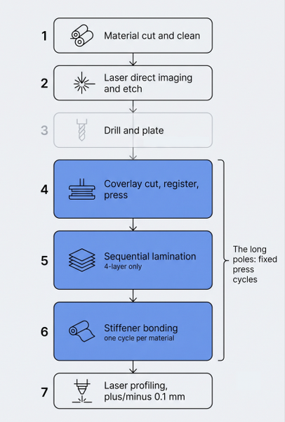
- Material cut and cleaned: Stocked polyimide is cut into a panel and micro-etched.
- Laser direct imaging and etch: Artwork is written onto dry film resist with per-panel scaling.
- Drill and plate: Double-sided and four-layer builds only.
- Coverlay cut, register, and press: Openings are laser cut, aligned, and then bonded in a heated press.
- Sequential lamination: Four-layer builds a bond between two cores, adding a press cycle.
- Stiffener bonding: Each material is a separate placement and bonding operation.
- Laser profiling: Outlines are cut to ±0.1 mm (±3.9 mil), tightening to ±0.05 mm on request.
Steps 4, 5, and 6 are the long poles. A press cycle takes the time it takes regardless of quantity, which is why a four-layer flex with three stiffener types will never match a single-layer bare flex.
Surface Finish and Electrical Testing
Flex uses ENIG almost universally because hot air solder leveling would deform thin polyimide on contact. ENIG is a wet chemistry line with a queue, so it behaves like a fixed block of hours rather than a per-board cost. Electrical test scales with your design instead: flying probe walks every net individually, so a 40-net sensor tail clears in minutes while a 400-net display flex takes far longer.
Key Factors Affecting Fast Turn Flex PCB Lead Time
Material Selection, Layer Count, and Circuit Complexity
Three decisions account for most of the variation in flex PCB lead time, and all three are made before you route a trace.
| Design Choice | Fast Lane Option | What Adds Days | Why |
| Layer count | 1 or 2 layers | 4 layers | Extra press cycle, tighter registration |
| Base material | Stocked 25 or 50 µm polyimide | LCP or specialty film | Material must be purchased in |
| Trace and space | 3.5/3.5 mil on 0.5 oz | 2/2 mil absolute limit | A scrapped panel means a rebuild |
| Copper weight | 18 µm (0.5 oz) | 35 µm (1 oz) with fine pitch | Needs wider features and a thicker coverlay |
| Construction | Adhesive-free polyimide | Mixed adhesive types | Extra bonding step |
Board Size, Panel Utilization, and Additional Processes
Regular flex production tops out around 234 x 490 mm (9.21 x 19.29 in), extending to 250 x 600 mm with edge rails and a support confirmation that adds a review step. The other end catches more people: boards below 20 x 20 mm should be panelized, and anything below 10 x 10 mm must be.
Bolt-on processes each add an operation: stiffener bonding, one cycle per material type; EMI shielding film at 18 µm, an extra lamination pass; adhesive tape applied separately; and a tighter ±0.05 mm outline tolerance, which slows laser profiling.
Engineering Review and Manufacturing File Quality
This is where fast turn orders actually die. An engineering query pauses your job until you reply, so files sent on a Friday afternoon can buy a three-day delay for a five-minute answer. One wearable sensor flex held for 41 hours because the stiffener drawing showed an FR4 pad on the top face, while the assembly drawing showed it underneath.
Mistake 1: No stiffener drawing. Nothing in a Gerber set tells the fabric which face a stiffener bonds to. To fix this: supply a mechanical layer showing outline, material, thickness, and face.
Mistake 2: Bend zones are undocumented. Vias and stiffener edges inside a fold look legal to a DRC check. To fix this: draw bend zones on a dedicated layer, following the flexible PCB bend radius rules.
Mistake 3: Coverlay openings drawn as solder mask. Coverlay is a cut film, so openings copied from a rigid-board mask layer are almost always too tight. To fix this: expand each aperture 0.1 mm one-sided and confirm 0.15 mm clearance to any trace.
How to Prepare Your Flex PCB Design for Faster Production?
Follow Flex PCB Design Rules for Manufacturing
Start from the fab's published numbers rather than your EDA tool's rigid-board defaults, because the two disagree in several places that matter.
| Rule | Standard Capability | Consequence of Ignoring It |
| Min trace and space, 0.33 oz | 3/3 mil (0.076 mm) | Yield loss and possible rebuild |
| Min trace and space, 0.5 oz | 3.5/3.5 mil | Etch undercut on fine features |
| Min trace and space, 1 oz | 4/4 mil (0.10 mm) | Shorts between conductors |
| Coverlay opening to trace | ≥ 0.15 mm | Exposed copper or a covered pad |
| Coverlay expansion | 0.1 mm one-sided | Adhesive squeezes onto pads |
| Static bend radius, 1 layer | ≥ 6x total thickness | Cracking at the fold crest |
| Static bend radius, multilayer | ≥ 10x total thickness | Delamination and fracture |
| Silkscreen character height | ≥ 1.0 mm (39 mil) | Illegible or clipped text |
| Via in bend zone | Never | Barrel cracks within dozens of cycles |
Route every trace perpendicular to the bend axis and keep plated holes out of the fold. This prevents more field failures than every other item combined.
Optimize Trace Width, Spacing, and Layer Stackup
Design at standard capability, not at the limit. If your routing closes at 3.5/3.5 mil on 0.5 oz copper, take it and leave the 2/2 mil limit for the one region that needs it. Pick a stackup the fab already lists, and keep copper balanced so the panel does not curl through lamination.
Impedance is where designers overreach. On a 25 µm polyimide core, a 50 Ω single-ended microstrip needs a trace around 48 µm (1.9 mil) wide, at the process limit where a ±20% tolerance destroys the impedance window. On a 50 µm core, the same target needs roughly 96 µm (3.8 mil). If your flex carries USB, MIPI, or LVDS, choose the 50 µm dielectric before routing.
Prepare Complete Gerber and Manufacturing Files
Send a package that answers every question before it is asked.
- Gerber RS-274X for every copper, coverlay, and silkscreen layer, plus an Excellon drill file.
- Board outline on a dedicated mechanical layer, as one closed contour.
- A bend zone layer showing every fold, with axis, radius, and static or dynamic.
- A stiffener drawing giving outline, material, thickness, and mounting face.
- A fabrication drawing carrying the stackup and tolerances. This is not optional on flex, because coverlay, stiffener, and bend information have nowhere else to live.
Fast Turn Flex PCB Panelization and SMT Assembly Considerations
Panel Design and Carrier Requirements for Flex PCB Assembly
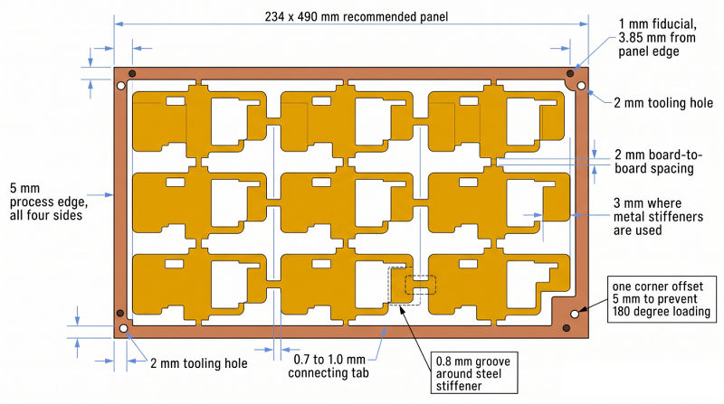
A bare flex circuit cannot be assembled. It has no stiffness, so a pick-and-place nozzle pushes it out of position, and a reflow conveyor will not hold it flat. The first answer is the panel: boards held in an array by narrow tabs inside a rigid frame.
| Panel Parameter | Specification | Why It Matters for Assembly |
| Recommended panel size | 234 x 490 mm | Matches the production frame |
| Minimum panel for SMT | 70 x 70 mm (2.76 in) | Below this, the conveyor rails cannot grip |
| Process edge, all four sides | 5 mm (197 mil) | Gives the conveyor something to hold |
| Board-to-board spacing | 2 mm standard | Room for the laser to cut |
| Spacing with metal stiffeners | 3 mm (118 mil) | Steel resists laser cutting |
| Connecting tab width | 0.7 to 1.0 mm (28 to 39 mil) | Holds firm, still depanels by hand |
| Groove around the steel stiffener | 0.8 mm (31 mil) | Let the laser form the outline cleanly |
The second answer is a carrier, or SMT pallet: a machined tray of synthetic stone or magnetic steel that holds the panel through printing, placement, reflow, and inspection.
Fiducial Marks and Positioning Requirements
Fiducials are how the placement machine finds your pads, and flex needs more of them than rigid does because polyimide stretches.
- Diameter: 1.0 mm solid copper circle, bare of solder mask or coverlay
- Placement: centered 3.85 mm (152 mil) from the panel edge, one per corner
- Asymmetry: offset one corner fiducial by at least 5 mm so the panel cannot be loaded or rotated
- Tooling holes: 2.0 mm diameter, non-plated, with matching asymmetry
- Keepout: 1 mm around each fiducial, 0.5 mm around each tooling hole
Panel fiducials alone are not enough. Add a local fiducial beside each circuit, because material stretch means the true position of unit 12 is not unit 1 plus a pitch. It earns its space twice: when the bare-board test finds a defective unit, the fab paints over that unit's fiducial so the machine skips it.
Warpage Control During SMT Assembly
Warpage on flex is a materials problem, not a handling problem. Polyimide expands far more than copper, so a panel heated to a 245 to 260 °C reflow peak moves in ways the copper pattern resists. It is also hygroscopic, which is why flex is baked before assembly, commonly for a few hours at 120 °C. Four controls keep a panel flat:
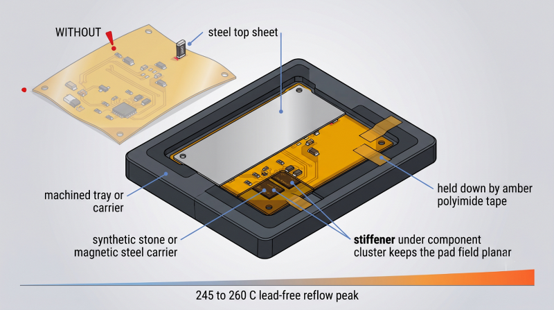
- Use more tabs, not wider ones. In steel-stiffened regions, aim for 1.0 mm tabs.
- Balance copper across the panel. A solid pour on one side guarantees a curl.
- Place stiffeners under component clusters, using the PCB stiffener selection guide to pick the material.
- Keep the carrier under the panel through cooling, and slow the preheat ramp.
Choosing a Fast Flex PCB Manufacturer
Manufacturing Capability and Production Capacity
Judge a fast flex PCB manufacturer on one question: Does flex run on their own line? A broker who subcontracts adds a margin and cannot answer a DFM question without relaying it. Ask for the numbers that constrain your design:
- Minimum trace and space at your copper weight, since 3 mil on 0.33 oz and 3 mil on 1 oz are different claims
- Whether four-layer runs on the same schedule as two-layer
- Maximum and minimum panel size, and whether they panelize for you
- Stated build time for flex, specifically, separate from their rigid FR4 number
Flexible Material, Stiffener Options, and Quality Control
Material breadth decides whether your design gets built as drawn or quietly value-engineered into something weaker. Confirm adhesive-free polyimide in both dielectric thicknesses and stiffeners in usable steps. Quality control matters more on flex because the defects hide: a hairline crack in a bend zone passes visual inspection and fails three weeks into the field trial. Confirm 100% flying probe net testing plus AOI, and ask which IPC-6013 class they build to. IPC-6013 governs qualification; IPC-2223 sets the design rules.
Prototype and Small-Batch Production Support
The transition from five pieces to five thousand is where flex programs lose the time they saved. If prototypes run on a different line or laminate, you requalify from zero. Ask three questions:
- Do prototype and production use the same laminate, copper, and coverlay?
- Does the panel layout carry over, or is it redrawn for volume?
- Can components be sourced in-house, or does the flex wait on your kitting?
That last point is the hidden delay. A four-day board waiting nine days for a connector has a thirteen-day lead time.
JLCPCB's Fast Turn Flex PCB Manufacturing Capabilities
Advanced LDI Technology for High-Precision FPC Production
JLCPCB images its flex lines with laser direct imaging, writing artwork onto dry film resist with per-panel scaling that compensates for polyimide movement. Removing the phototool is a large part of why the published flex build time is 4 to 5 days.
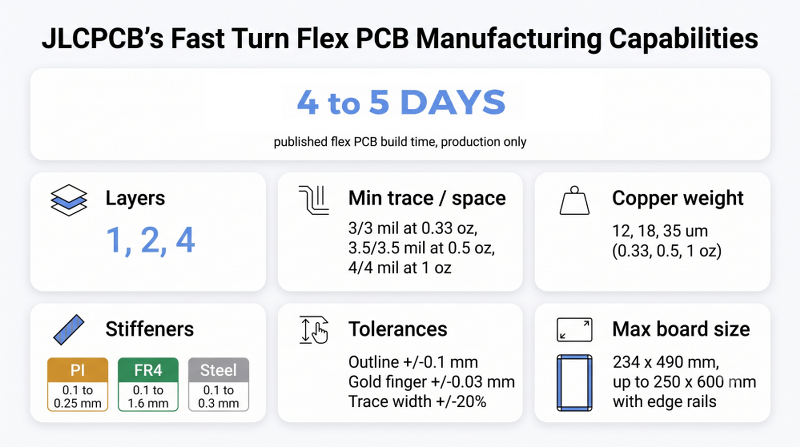
The capability set behind that schedule is public. Minimum trace and space runs 3/3 mil on 0.33 oz copper, 3.5/3.5 mil on 0.5 oz, and 4/4 mil on 1 oz, with trace width held to ±20%. Plated holes span 0.1 to 6.5 mm (3.9 to 256 mil) at ±0.08 mm, outlines cut to ±0.1 mm, and gold fingers hold ±0.03 mm.
Adhesive-Free PI Material and Multiple Stiffener Options
The standard substrate is adhesive-free polyimide in 25 µm and 50 µm dielectric thicknesses, the construction that best survives repeated lamination and dynamic bending. Transparent PET at 36 µm is available for one and two-layer builds. The rest of the menu is stocked:
- Copper weight: 12 µm (0.33 oz), 18 µm, and 35 µm
- Coverlay color: yellow, black, white, or transparent
- Polyimide stiffener: 0.1, 0.15, 0.20, 0.225, and 0.25 mm
- FR4 stiffener: 0.1 to 1.6 mm (3.9 to 63 mil) in eight steps
- Stainless steel: 0.1, 0.2, and 0.3 mm; adhesive tape: 3M9077, 3M468, tesa8854
- Surface finish: ENIG, in 1 or 2 microinch gold
That menu makes the connector fit inside one build. A 0.5 mm pitch ZIF connector, such as the Hirose FH12, specifies an insertion thickness around 0.30 mm ±0.05 mm, so a 0.12 mm (4.7 mil) two-layer flex plus a 0.2 mm polyimide stiffener lands at 0.32 mm.
Rapid Prototyping, DFM Review, and Production Support
Automated DFM analysis runs against your uploaded files before tooling begins, and catching a tight coverlay clearance or a via in a bend zone at the quote stage is usually worth more than the entire order. Panels can also be laid out for you with process edges and fiducials already corrected for SMT.
If your flex needs components, SMT assembly runs on the same order with parts from the JLCPCB parts library. Upload your Gerbers to the instant quote system to see build time, price, and DFM feedback together.
Conclusion
Fast turn flex PCB service does not work by running the same process quicker. It works by removing the things that wait: the laminate order, the phototool, the punch die, and the CAM engineer's queue. Those savings survive only as long as your design stays inside the menu that made them possible.
Your files, not the factory, usually set your delivery date. A complete package with a bend zone layer, a stiffener drawing, and a fabrication note clears automated review and enters production the same day.

Frequently Asked Questions About Fast Turn Flex PCB
How fast can a flex PCB prototype be manufactured?
Ans: JLCPCB publishes a build time of 4 to 5 days for flexible PCBs, measured from the start of physical production to the point the boards reach the shipping center. That excludes order review, typically around 30 minutes, and it excludes transit.
What factors affect flex PCB lead time?
Ans: Layer count is the largest single factor, since four-layer builds add a lamination press cycle. Non-stocked materials, absolute-limit trace and space, multiple stiffener types, and tighter outline tolerances each add operations. The most common delay is an ambiguous file set that triggers an engineering query.
Is a fast-turn flex PCB more expensive than a standard flex PCB?
Ans: Not necessarily, because fast turn is a different production path rather than a rush surcharge. Speed comes from stocked materials, laser direct imaging, and automated review, all of which remove cost as well as time. What raises the price is the complexity that also slows you down.
What files are required for fast-turn flex PCB manufacturing?
Ans: Send Gerber RS-274X for all copper, coverlay, and silkscreen layers, an Excellon drill file, and the board outline on a mechanical layer. Flex needs three extras: a bend zone layer, a stiffener drawing giving material, thickness, and mounting face, and a fabrication drawing carrying the stackup.

Popular Articles
• Choosing the Right Bend Radius for Durable Flexible PCBs
• Flexible Meets Durable: Understanding Rigid-Flex PCB Technology
• PCB Stiffeners: An Essential Requirement for Flexible Circuits
• The Ultimate Guide to Flexible PCB: Types, Design, and Applications
• 45 Must-Know Flex PCB Design Tips You Can't Afford to Miss!
Keep Learning
Choosing the Right Bend Radius for Durable Flexible PCBs
Key Takeaways Mastering the bend radius is essential for reliable flexible PCB design. Following IPC-2223 guidelines, maintain a minimum of 6× total thickness for static bends and 100× for dynamic applications, while using thinner RA copper, adhesiveless polyimide, staggered traces, and cross-hatched patterns in flex zones. Proper material selection, layer stackup optimization, and adequate clearance from stiffeners can dramatically extend flex life and prevent premature trace cracking or delamination......
Flex PCB Stackup Design Guide: Layers, Materials & Reliability
Key Takeaways A reliable flex PCB starts with the right stackup design. The layer structure, material selection, and copper arrangement directly affect flexibility, bend life, electrical performance, and manufacturing reliability. This guide explains single-sided, double-sided, and multilayer flex PCB stackups, including polyimide materials, coverlay, copper types, and key design considerations for creating durable flexible circuits with JLCPCB. Did you ever wonder how a foldable phone can last for 20......
Flexible Meets Durable: Understanding Rigid-Flex PCB Technology
In the rapidly evolving world of electronics, the demand for smaller, more reliable, and more versatile devices continues to grow. To meet these demands, engineers and designers are increasingly turning to Rigid-Flex PCBs. The circuit boards combine rigid and flexible substrates into a single interconnected structure. This combination allows for complex designs that can bend and flex in specific areas while maintaining rigidity in others. To manufacture rigid flex PCBs, IPC offers advice and best prac......
PCB Stiffeners: An Essential Requirement for Flexible Circuits
A printed circuit board stiffener plays an important role when it comes to offering mechanical support to a PCB. They are particularly helpful for flexible circuit boards, that given their name, are flexible and in need of stiffness in certain places. Stiffeners are particularly required when components are placed in a flex zone & the weight of these components stresses the flex material. These components provide a rigid connection from the flexible portion to the solid board. This solidity makes appl......
The Ultimate Guide to Flexible PCB: Types, Design, and Applications
Key Takeaways JLCPCB 1–4 Layer Flex PCB: Supports 1 to 4-layer FPCs with polyimide (PI) substrates and trace/space down to 3/3 mil. Stiffener Selection: Use PI (0.1–0.25mm) for ZIF connectors, FR4 (0.1–1.6mm) for SMT support, and Stainless Steel (0.1–0.3mm) for high rigidity. Layout Optimization: Use cross-hatched copper ground planes and stagger 2-layer traces to eliminate the "I-Beam effect." Surface & Protection: Combine Immersion Gold (ENIG 1u"/2u") for SMT planarity with flex coverlay to protect ......
Medical Flex Circuits: Manufacturing, Applications, Materials, and Design Guide
Medical flex circuits made to fit inside a 1.0 mm disposable endoscope, wrap around a hearing aid shell, and sit on a patient's arm for ten straight days. When one fails, it is not a warranty return but a device history file and a regulatory conversation. In this guide, you will learn: What separates a medical flex circuit from a consumer one How they are built, tested, and released Polyimide, copper, coverlay, and stiffener choices Fine line, bend radius, and layer count limits What to check before c......