FPC Electronics: What Is It, How It Works, Applications, and Benefits
17 min
- How Does FPC Work in Electronics?
- Key Materials Used in FPC Electronics
- How Are FPC Electronics Manufactured?
- Advantages and Applications of FPC Electronics
- FPC Electronics vs Traditional PCB Solutions
- Key Design Considerations for FPC Electronics
- Choosing an FPC Electronics Manufacturer
- Conclusion
- Frequently Asked Questions About FPC Electronics
FPC electronics is the reason your phone camera still works after a hundred open-and-close cycles. Peel apart almost any modern device, and you will find a thin amber ribbon carrying signals around corners no rigid board could turn.
In this guide, you will learn:
- What does FPC stand for, and what are the differences between FFC and FPC?
- A flexible circuit that conducts a signal as it flexes
- The materials include one polyimide, copper, coverlay, and stiffener
- FPC manufacturing process (etching to electrical tests)
- The advantage of FPC over a rigid board or wire harness is that it can be bent
- What Is FPC Electronics?
FPC (Flexible Printed Circuit)
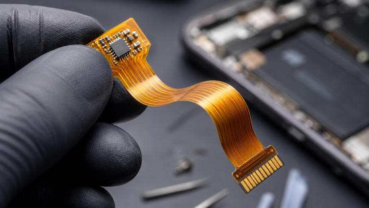
An FPC (flexible printed circuit) is a printed circuit with copper conductors etched into a thin polymer film (as opposed to a glass-epoxy board), which means the completed circuit can be bent, folded, and wrapped around the inside of a product. Single-layer FPC is generally 0.07 mm (2.8 mil) thick, similar to printer paper. The copper, pads, and netlist are identical to those on any PCB; only the carrier was changed.
What Does FPC Mean in Electronics?
There are at least three meanings of FPC, and you have to deduce it from the context.
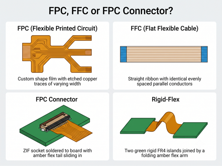
- FPC, also known as flex PCB or flex circuit, is an etched, custom-shaped copper circuit on polyimide film, made to your artwork.
- FFC, or flat flexible cable: a stock ribbon of parallel conductors bought by pitch and conductor count. A catalog item, not a designed part.
- FPC connector: the zero insertion force socket on the rigid board that a flex tail slides into.
- Rigid-flex: rigid FR4 islands laminated to flex arms as one continuous part.
How FPC Works in Electronic Devices
An FPC serves as two in one inside a product. It transmits signals, like a circuit board, and serves as a mechanically active element, such as a cable, thus substituting for a connector, a cable, and a second connector. Take a look at the back camera of nearly any smartphone: the sensor is on a stiffened "island", a thin flex arm bends under the display, and a gold-plated tail plugs into a ZIF socket. Three mechanical faults and one etched component.
How Does FPC Work in Electronics?
Signal Transmission Through Flexible Circuit Layers
From an electrical point of view, nothing out of the ordinary occurs. The etched copper conducts the current in the same way as it does on a rigid board, and the polyimide is just the insulating material that separates the conductors. DuPont Kapton HN is lower-loss than FR4 near 4.3 GHz, with a dielectric constant of 3.4 and a dissipation factor of 0.0018 on 25 µm (1 mil) film at 1 kHz. The problems that come back haunt people! A single-layer flex does not have a reference plane, and any return current you route takes the path of least resistance home.
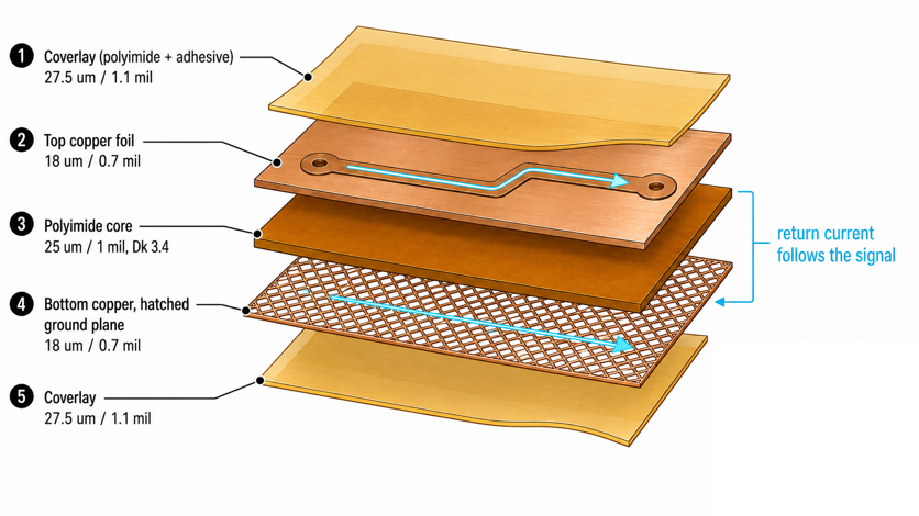
A first-flight FPV drone build revealed rolling bars in the video during the spool-up of the motors. The camera supplied a 100 mm single-layer flex with all the signals except one thin edge ground, and all the signals were being fed back through the same conductor, thus introducing motor noise into the video. A two-layer flex-hatched ground cleared it.
Flexible Routing for Compact Electronic Designs
The routing benefit is three-dimensional. A rigid board forces every net into a flat plane, so joining two boards means a header pair plus mating depth, often 6 to 10 mm (236 to 394 mil) of dead vertical space. An FPC folds into under 1 mm, doing the same job, and every connector pair you delete buys back roughly 3 to 5 mm of Z-height. It can also follow a curved housing wall or wrap a battery.
Mechanical Flexibility and Reliability of FPC
When a flex circuit bends, the outer surface stretches and the inner surface compresses, while one plane in the middle sees almost no strain. That plane is the neutral axis, and flex reliability is largely the art of keeping copper near it.
Two variables dominate. The total thickness is a determination of the strain that the outer copper experiences; thus, the minimum bend radius is expressed as a multiple of finished thickness: 6x for a single-layer static bend and 10x for a multi-layer bend. Whether that strain cracks anything depends on the structure of the grain—rolled annealed copper has flat elongated grain that lends itself to being folded, whereas electrodeposited copper has columnar grain that seeds cracks. First, characterize the bend as either static or dynamic, since the multipliers are an order of magnitude different.
Key Materials Used in FPC Electronics
Polyimide Film as the Main Flexible Substrate
Almost all the FPCs produced are based on polyimide film, which most engineers still refer to as "Kapton." Polyester is more affordable but will not stand up to soldering lead-free reflow at 245-260°C, or short excursions up to 400°C.
Materials covered by IPC-4204 come in two constructions:
- Adhesive-based (three-layer): Copper, acrylic adhesive, then polyimide. Cheaper, but the acrylic expands strongly in the Z axis and pushes on plated via barrels during reflow.
- Adhesive-free (two-layer): Copper bonded directly to the polyimide. Thinner, steadier through repeated lamination, and better at high frequency.
Anything that reflows twice, folds in service, or carries signals above a few gigahertz belongs on adhesive-free polyimide.
Copper Layers for Electrical Performance
Copper on an FPC is a grain-structure decision before it is a thickness decision. Foil weight then sets the smallest feature the etcher can hold, because thicker copper undercuts more sideways.
| Copper Weight | Foil Thickness | Typical Min Trace/Space | Best Suited For |
| 0.33 oz | 12 µm (0.5 mil) | 0.076/0.076 mm (3/3 mil) | Fine-pitch camera and display tails, 4-layer flex |
| 0.5 oz | 18 µm (0.7 mil) | 0.089/0.089 mm (3.5/3.5 mil) | General signal routing is the default choice |
| 1 oz | 35 µm (1.4 mil) | 0.10/0.10 mm (4/4 mil) | Power rails, LED strings, battery, and motor links |
Coverlay and Stiffener Options for Different Applications
Flex circuits do not use liquid solder mask. The protective layer is a coverlay, a polyimide film pre-coated with adhesive and pre-cut with openings that expose only the pads, specified under IPC-4203. Yellow is standard, with black to hide traces, white to reflect light, and transparent for inspection. Stiffeners add local rigidity where the circuit must not flex, and mixing types on one part is normal.
- Polyimide, 0.1 to 0.25 mm (4 to 10 mil): Brings a ZIF tail up to the connector's clamp thickness.
- FR4, 0.1 to 1.6 mm (4 to 63 mil): Component islands, screw-down bosses, heavy connectors.
- Stainless steel, 0.1 to 0.3 mm (4 to 12 mil): Maximum rigidity in minimum height.
- PSA adhesive film, 0.05 to 0.13 mm (2 to 5 mil): Bonds the flex to a housing or battery pack.
How Are FPC Electronics Manufactured?
Circuit Pattern Formation and Precision Etching Process
FPC fabrication is subtractive: you start with a copper-clad film and chemically remove everything that is not a conductor.
- Clean and micro-etch the copper-clad polyimide so the resist adheres.
- Laminate dry film resist across the panel under heat and roller pressure.
- Imagine the artwork on the resist, on modern lines, using laser direct imaging.
- Develop and spray etch down to the polyimide, then strip the remaining resist.
The step engineers argue about is imaging, not etching. Polyimide moves with humidity and shrinks once the copper restraining it is etched away, and laser direct imaging can scale the artwork per pane, whereas a fixed film cannot.
Lamination, Coverlay, and Multi-Layer Assembly
The pre-cut coverlay is registered over the circuit and pressed in a heated hydraulic press, where the adhesive must fill the gaps between traces without squeezing into the pad openings. That is why coverlay apertures are drawn about 0.1 mm (4 mil) larger than the pad on each side. Multilayer flex adds vias before this stage. Holes are drilled or laser-ablated, metalized, and plated to join the layers, on a substrate that moves between operations. That movement is why layer-to-layer registration, not trace width, limits four-layer flex.
Surface Finishing and Electrical Testing
Exposed pads then receive a finish, almost always ENIG at 1 or 2 microinches of gold, flat enough for fine-pitch reflow and hard enough to survive repeated ZIF insertions. Testing has two halves that beginners conflate. Electrical proof is automated optical inspection plus 100% net testing. Mechanical proof is separate: flexural endurance is measured per IPC-TM-650 Method 2.4.3 (the MIT fold test), and acceptance classes are defined in IPC-6013.
Advantages and Applications of FPC Electronics
Thin and Lightweight Design for Space-Saving Electronics
An FPC replaces the conductor, the insulation, the crimp terminals, the connector housings, and the cable ties with a film a fraction of a millimeter thick.
- Mass: typically a 60 to 75% reduction against an equivalent wire harness.
- Part count: one etched circuit replaces two connectors, a cable, and every crimp.
- Assembly time: a stiffened tail drops into a ZIF latch in about a second.
Improved Reliability for Flexible and Dynamic Applications
Less interconnection results in fewer points of failure. Each crimp, splice, and mating pair removed is one joint that cannot corrode, fret, or back out under vibration. Repeatability is the second argument. The standard position of all conductors on each unit is achieved with an etched circuit to enable controlled impedance and predictable crosstalk within the moving assembly.
Consumer Electronics, Medical, Automotive, and IoT Applications
There is marked sectoral variation in the motives for flex.
- Consumer electronics: smartphone camera tails, laptop display cables, foldable hinges. The design is determined by dynamic bend life and stack height.
- Medical: tips for ultrasound probes, endoscopes, ECGs, glucose patches, and hearing aids. Miniaturization and biocompatibility are the prime aspects.
- Automotive: LED tail lamps, dashboard clusters, seat mats, battery cell connection systems. The thermal cycling and vibration spec is set.
- Printing: printer carriage cables, robot joint wiring, and machine vision heads. The level of cycles determines the selection.
Adhesive-free polyimide and IPC-6013 Class 3 acceptance are typically associated with medical and automotive programs, and are determined at the schematic stage.
FPC Electronics vs Traditional PCB Solutions
FPC vs Rigid PCB
It doesn't mean that technology will supersede the other, and assuming flex is a one-size-fits-all upgrade is the quickest route to overspending. Rigid FR4 is less expensive per sq cm, has a higher layer count, and can mount heavy components without reinforcement.
| Factor | FPC | Rigid PCB | Practical Consequence |
| Substrate | Polyimide film, Dk 3.4 | FR4 glass-epoxy, Dk ~4.3 | Flex is the lower-loss dielectric |
| Typical thickness | 0.07 to 0.45 mm (2.8 to 17.7 mil) | 0.6 to 2.0 mm (24 to 79 mil) | Flex fits gaps ,rigid boards cannot |
| Layer count | 1, 2, or 4 in mainstream production | 2 to 20+ | Dense digital designs still belong on rigid |
| Component support | Needs a stiffener under any component field | Supports heavy parts directly | Flex assembly needs mechanical planning |
| Bare-board cost | Higher per unit area | Lower per unit area | Compare at the assembly level, not the board level |
| Best for | Folds, curves, hinges, weight-critical builds | Flat boxes, high layer counts, real power dissipation | Match the technology to the mechanical envelope |
FPC vs Wire Harness
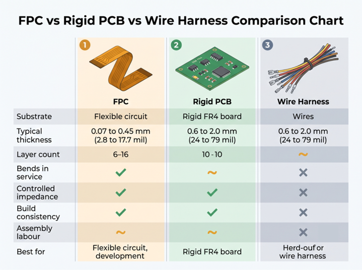
A wire harness wins on exactly one axis: no tooling and easy field changes, which keeps it ahead for one-offs. Once any volume exists, everything else favors the etched circuit. Fixed geometry is the technical difference. A harness with uncontrolled spacing and coupling only allows flex supports to provide reliable high-speed lanes and repeatable EMC results. On the line, one tail drops into a ZIF latch instead of crimp, insert, dress, tie, and inspect.
Key Design Considerations for FPC Electronics
Layer Count, Circuit Density, and Trace Design
Choose the fewest layers your signals need, because every added layer costs bandwidth and performance. A four-layer build at 0.20 to 0.45 mm is a routing solution rather than a bending one. Then design to the fabricator's real numbers rather than your EDA tool defaults. Pushing below the trace and space limit for your copper weight costs yield, so check your densest fanout against the figure for the foil you specified.
Bend Radius and Mechanical Requirements
Bend radius decides whether your flex lives or dies, and it is set as a multiple of total finished thickness. IPC-2223, the sectional design standard for flexible printed boards, defines those multipliers and the bend-area conductor rules. Even careful designers repeat the same three errors:
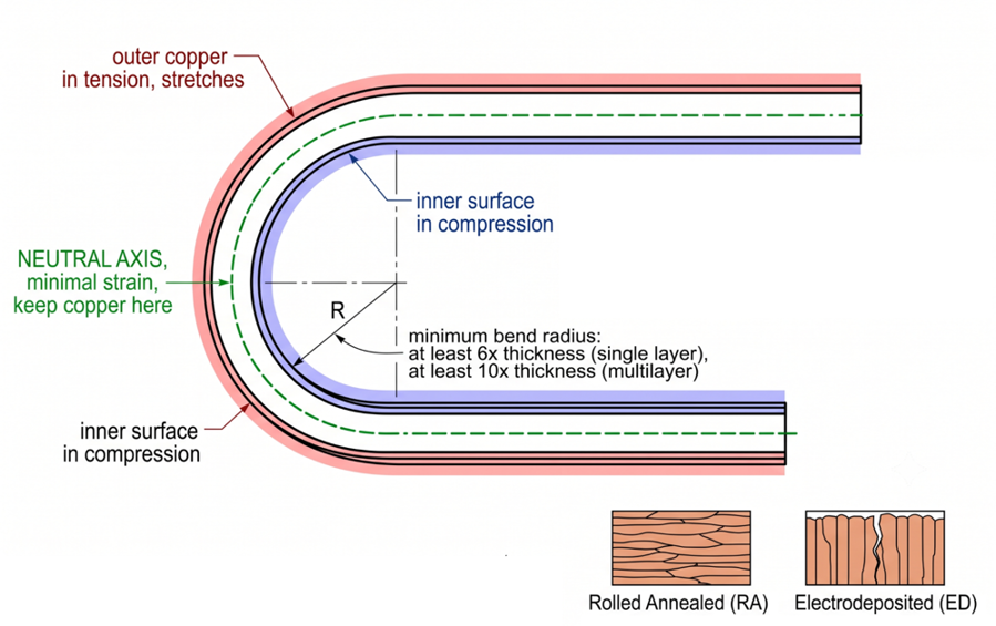
Mistake 1: Placing a via or plated hole inside the bend zone. A drilled barrel is a rigid inclusion in a bending film, and the copper knuckle at its rim is a stress riser. To fix this: keep every via at least 1 mm clear of where bending begins.
Mistake 2: treating one bend radius as good for all motions. An installation fold and a hinge cycling thousands of times differ by an order of magnitude. To fix this, classify the bend as static or dynamic, then apply the multiplier with a 20-30% margin.
Mistake 3: running traces diagonally across the fold line. A diagonal conductor sees bending and shear strain at once. To fix this: run every trace perpendicular to the bend axis.
Stiffener Selection and Assembly Requirements
Stiffener choice becomes an exact fit problem the moment a connector is involved. Most 0.5 mm pitch ZIF connectors require an insertion thickness of 0.30 mm ± 0.05 mm (11.8 ± 2 mil), and a bare two-layer flex at 0.12 mm (4.7 mil) is far too thin to develop sufficient contact force.
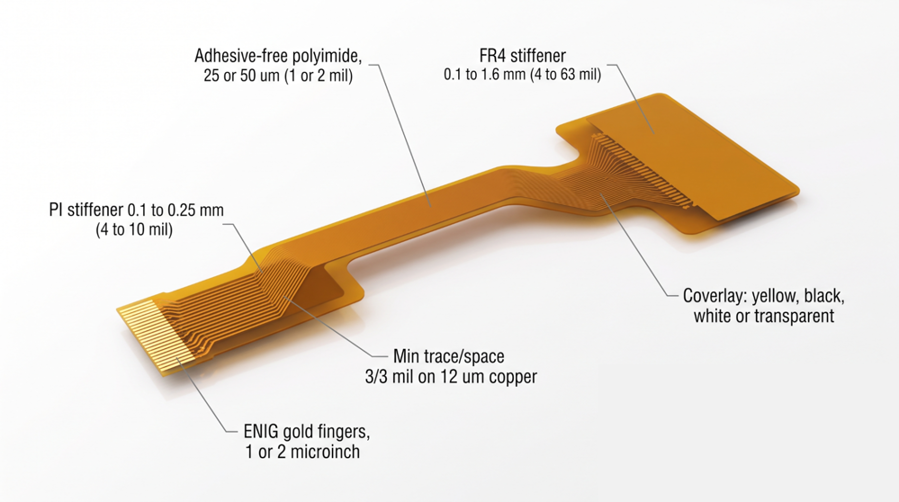
To fix this: bond a stiffener to the face opposite the contact fingers, sized as the connector target minus your finished flex thickness. A 0.12 mm flex plus a 0.2 mm polyimide stiffener totals 0.32 mm, within the window.
Assembly adds two rules: component fields need a stiffener beneath them so the circuit stays flat through reflow, and the coverlay must be opened over ZIF contact fingers.
Choosing an FPC Electronics Manufacturer
Manufacturing Capability and Quality Control
Match a supplier's published limits against your worst feature, not your average one. Ask for minimum trace and space at your specific copper weight, supported layer counts, minimum via diameter, and profile tolerance. Then ask how they prove the board is good: 100% net testing, AOI, and a stated IPC-6013 class. A quoted minimum trace width means nothing without the copper weight attached. Three mil on 0.33 oz and three mil on 1 oz are not the same claim.
Material Options and Customization Support
A genuine flex shop offers choices rather than one recipe. Confirm they stock both adhesive and adhesive-free polyimide, both copper grain types, and stiffeners in usable steps. You also want a supplier who tells you a 0.15 mm (6 mil) bend radius is impossible on a four-layer stack before building it.
The jump from five pieces to five thousand is where flex projects lose time. Confirm that prototypes use identical laminate and copper to production, that tooling carries over, and that the shop can reflow components onto the flex.
JLCPCB's Advanced FPC Manufacturing Capabilities
JLCPCB offers one-, two-, and four-layer FPC as a standard catalog service, so the numbers below are published rather than negotiated per quote.
| Capability | Specification | What It Means for Your Design |
| Layer count | 1, 2, and 4 layers | A simple jumper through a referenced signal stack |
| Finished thickness | 0.07 to 0.45 mm | Sets your minimum bend radius before you route |
| Copper weight | 12, 18, 35 µm (0.33, 0.5, 1 oz) | Trade fine pitch against current capacity |
| Min trace/space | 3/3 mil on 12 µm, 3.5/3.5 mil on 18 µm, 4/4 mil on 35 µm | Your densest fanout must clear this |
| Min via hole | 0.30 mm standard, 0.10 mm (3.9 mil) on 2-layer | How tight a crossover can get |
| Surface finish | ENIG, 1 or 2 microinch gold | Flat pads for fine pitch and ZIF insertion |
| Outline tolerance | ±0.1 mm (±4 mil), ±0.05 mm on request | Whether the part drops into your housing |
| Max panel size | 234 x 490 mm (9.2 x 19.3 in) | Ceiling on long cable-style parts |
LDI Technology for High-Precision FPC Fabrication
The flex lines image was produced using a dry-film process with laser direct imaging, which is why the fine-pitch numbers above hold. LDI writes artwork directly onto the resist without a phototool, so it can scale each panel to compensate for the polyimide movement described earlier.
Adhesive-Free PI Material and Multiple Stiffener Options
The standard substrate is adhesive-free polyimide in 25 µm and 50 µm (2 mil) dielectric thicknesses, the construction that survives repeated lamination and bending best. Transparent PET is available at 36 µm, where light must pass through the circuit, and an 18 µm black EMI shielding film can replace a metal can over a routed signal run.
Stiffeners span polyimide, FR4, stainless steel, and pressure-sensitive films across the full 0.05 to 1.6 mm range, so a ZIF tail, a component island, and a housing bond can live on one part. Pull components from the JLCPCB parts library, and price the build through the instant online quoting system.
Conclusion
The most useful thing to carry away is that a flexible printed circuit is not a cable that happens to conduct. It is a printed circuit board with the same copper, the same etching physics, and the same design rules, built on a substrate that bends.
Get four things right, and the technology repays you: choose the fewest layers your signals need, classify every bend as static or dynamic before applying a radius multiplier, use rolled annealed copper anywhere that moves, and add stiffeners where mechanics demand support rather than thickening the whole circuit.

Frequently Asked Questions About FPC Electronics
What is FPC in electronics?
Ans: FPC stands for flexible printed circuit, a printed circuit whose copper conductors are etched onto thin polyimide film instead of rigid glass-epoxy. It works electrically like any PCB, but bends and folds to fit inside a product. Watch the context, because "FPC connector" means the socket a flex tail plugs into.
What are FPC electronics used for?
Ans: FPCs are used wherever a circuit has to fit a shape rather than a plane: smartphone camera and display tails, laptop hinge cables, printer carriage cables, hearing aids, wearable patches, and automotive LED arrays. They also replace wire harnesses wherever weight or build repeatability matters.
What is the difference between FPC and PCB?
Ans: An FPC is a type of PCB built by the same etching process, so the real difference is the substrate. An FPC uses polyimide film at 0.07 to 0.45 mm and bends, while a rigid PCB uses FR4 at 0.6 to 2.0 mm and does not. Rigid supports more layers; flex fits curves and hinges.
Are FPCs reliable for electronic devices?
Ans: Yes, often more reliable than the wired alternative, because every connector and crimp deleted is a failure point removed. Reliability rests on three choices: bend radius above the standard multiple of thickness, rolled annealed copper for anything dynamic, and no vias in bend zones.

Popular Articles
• Choosing the Right Bend Radius for Durable Flexible PCBs
• Flexible Meets Durable: Understanding Rigid-Flex PCB Technology
• PCB Stiffeners: An Essential Requirement for Flexible Circuits
• The Ultimate Guide to Flexible PCB: Types, Design, and Applications
• 45 Must-Know Flex PCB Design Tips You Can't Afford to Miss!
Keep Learning
Choosing the Right Bend Radius for Durable Flexible PCBs
Key Takeaways Mastering the bend radius is essential for reliable flexible PCB design. Following IPC-2223 guidelines, maintain a minimum of 6× total thickness for static bends and 100× for dynamic applications, while using thinner RA copper, adhesiveless polyimide, staggered traces, and cross-hatched patterns in flex zones. Proper material selection, layer stackup optimization, and adequate clearance from stiffeners can dramatically extend flex life and prevent premature trace cracking or delamination......
Flex PCB Stackup Design Guide: Layers, Materials & Reliability
Key Takeaways A reliable flex PCB starts with the right stackup design. The layer structure, material selection, and copper arrangement directly affect flexibility, bend life, electrical performance, and manufacturing reliability. This guide explains single-sided, double-sided, and multilayer flex PCB stackups, including polyimide materials, coverlay, copper types, and key design considerations for creating durable flexible circuits with JLCPCB. Did you ever wonder how a foldable phone can last for 20......
Flexible Meets Durable: Understanding Rigid-Flex PCB Technology
In the rapidly evolving world of electronics, the demand for smaller, more reliable, and more versatile devices continues to grow. To meet these demands, engineers and designers are increasingly turning to Rigid-Flex PCBs. The circuit boards combine rigid and flexible substrates into a single interconnected structure. This combination allows for complex designs that can bend and flex in specific areas while maintaining rigidity in others. To manufacture rigid flex PCBs, IPC offers advice and best prac......
PCB Stiffeners: An Essential Requirement for Flexible Circuits
A printed circuit board stiffener plays an important role when it comes to offering mechanical support to a PCB. They are particularly helpful for flexible circuit boards, that given their name, are flexible and in need of stiffness in certain places. Stiffeners are particularly required when components are placed in a flex zone & the weight of these components stresses the flex material. These components provide a rigid connection from the flexible portion to the solid board. This solidity makes appl......
The Ultimate Guide to Flexible PCB: Types, Design, and Applications
Key Takeaways JLCPCB 1–4 Layer Flex PCB: Supports 1 to 4-layer FPCs with polyimide (PI) substrates and trace/space down to 3/3 mil. Stiffener Selection: Use PI (0.1–0.25mm) for ZIF connectors, FR4 (0.1–1.6mm) for SMT support, and Stainless Steel (0.1–0.3mm) for high rigidity. Layout Optimization: Use cross-hatched copper ground planes and stagger 2-layer traces to eliminate the "I-Beam effect." Surface & Protection: Combine Immersion Gold (ENIG 1u"/2u") for SMT planarity with flex coverlay to protect ......
Medical Flex Circuits: Manufacturing, Applications, Materials, and Design Guide
Medical flex circuits made to fit inside a 1.0 mm disposable endoscope, wrap around a hearing aid shell, and sit on a patient's arm for ten straight days. When one fails, it is not a warranty return but a device history file and a regulatory conversation. In this guide, you will learn: What separates a medical flex circuit from a consumer one How they are built, tested, and released Polyimide, copper, coverlay, and stiffener choices Fine line, bend radius, and layer count limits What to check before c......