Unlocking Smaller, Smarter PCBs with Embedded Passive Components
11 min
- What Embedded Passive Components Are and Why They Matter
- Major Benefits for Modern Electronic Designs
- Design Considerations for Successful Embedding
- Precision Manufacturing of Embedded Passive Components
- JLCPCB's Expertise in Embedded Passive Component PCBs
- Frequently Asked Questions (FAQ)
- Conclusion
Key Takeaways
Embedded passive components are revolutionizing PCB design by integrating resistors, capacitors, and inductors directly into the board layers. This technology delivers smaller, thinner, and higher-performance boards with up to 30-50% space savings, significantly reduced parasitic inductance, superior signal integrity at high frequencies, better thermal distribution, and enhanced reliability through fewer solder joints. Ideal for 5G, wearable, automotive, and RF applications, embedded passives turn miniaturization challenges into competitive advantages when designed with proper stackup, DFM, and advanced manufacturing support.
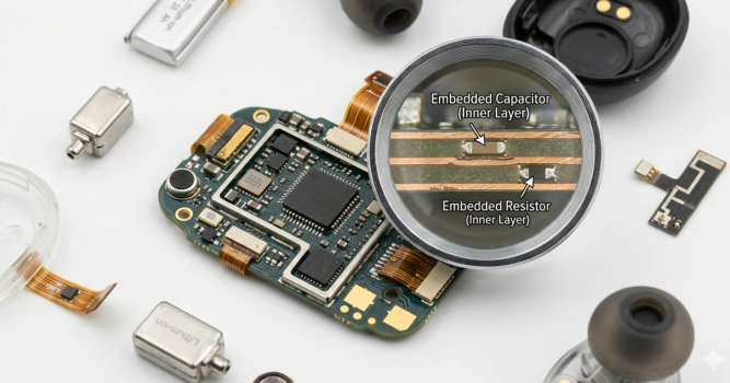
Have you ever taken apart a smartwatch or wireless headphones and wondered how all of the features are packed into such a small form factor? One of the keys to this is a technology that is revolutionizing the design of printed circuit boards (PCBs). With embedded passive components, it's possible to embed resistors, capacitors, and even inductors in the layers of a printed circuit board, instead of taking up precious space on the surface of the board where hundreds of individual components would normally be placed.
This matters more than ever. Our consumer devices are ever smaller and thinner, 5G networks require shorter signal traces, and automotive radar devices need to deliver millimeter wave functionality in a small package. In this article, we will look at what embedded passive components (embedded passives) are, why they are important in enabling the next generation of electronics, and how to design and build printed circuit boards (PCBs) that leverage the benefits of embedded passives.
What Embedded Passive Components Are and Why They Matter
Definition and Types of Embedded Passives in PCBs
An embedded passive component is a resistor, capacitor, or inductor that is incorporated or embedded within the PCB substrate instead of being placed on top of the board. Rather than being placed on a pad on the top or bottom layer, the component is embedded between two copper layers, or within the prepreg or core.
The three main types used in today's PCB manufacturing include:
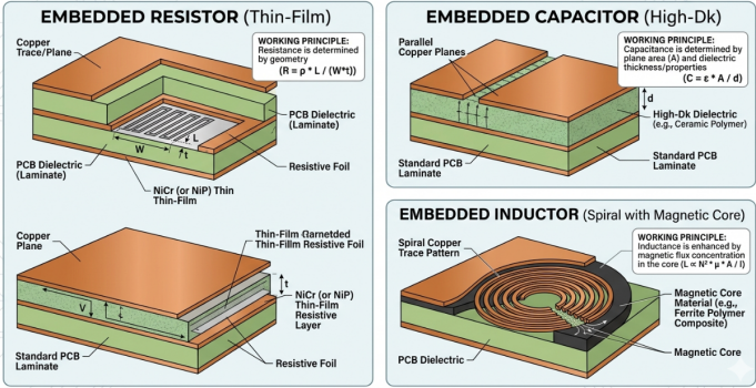
- Embedded Resistors: Formed from thin-film resistive materials like nickel-phosphorus (NiP) alloys or carbon-based ink applied to an internal copper layer. Common sheet resistivities are between 25 and 250 ohms per square for NiP alloys, and 1,000 ohms per square for carbon films.
- Embedded Capacitors: Created with thin layers of high-permittivity dielectric materials between two copper layers. Using materials such as barium titanate-filled epoxy or capacitive laminates (e.g., Oak-Mitsui FaradFlex) yields capacitance ranges of 1 to 5 nF per square centimeter.
- Embedded Inductors: Formed by creating spiral or meander shapes on inner layers. Rare because it's hard to get high inductance in a flat trace, but suitable for low-value RF inductors (1 to 50 nH).
Key Drivers: Miniaturization, Performance, and Cost Reduction
Designers are driven to embedded passives by three factors. First, miniaturization. A 0402 SMD capacitor consumes around 1.0 x 0.5 mm of space, plus pads and clearance. That's hundreds of decoupling capacitors on a typical BGA breakout board, and the surface area taken up by passives alone is vast.
The second factor is electrical. All surface-mount components have parasitic inductance in their solder joints and pads. A typical 0402 MLCC has a mounted inductance of 0.5-1.2 nH. At frequencies over 1 GHz, these parasitics undermine decoupling performance and cause resonance. Embedding capacitors between power and ground planes effectively eliminates this loop.
The third factor is cost-effectiveness in the long run. The initial cost of the board is higher, but you have fewer placements and solder joints to inspect, and smaller boards that result in more parts per panel. And the cost savings add up in high volume.
Major Benefits for Modern Electronic Designs
Reduced Board Size and Improved Signal Integrity
Integrating decoupling capacitors and termination resistors can reclaim 30-50 percent of the board space wasted on discrete passives. This extra space can be translated into a smaller product or used to add more functionality to the board.
Signal integrity improves in measurable ways:
| Parameter | Discrete 0402 MLCC (Surface) | Embedded Planar Capacitor |
|---|---|---|
| Mounted Parasitic Inductance | 0.5 - 1.2 nH | < 0.05 nH |
| Effective Decoupling Frequency | Up to ~500 MHz | Up to 3+ GHz |
| Via Stub to Power Plane | 0.2 - 1.0 mm | 0 mm (direct connection) |
| Solder Joints per Component | 2 | 0 |
| Surface Area per Component | ~1.2 mm squared | 0 mm squared |
The low parasitic inductance ensures the power delivery network has low impedance at higher frequencies. This is essential for today's processors with fast slew-rate transient currents (above 1 A/ns).
Enhanced Thermal Management and Reliability
Large numbers of small surface-mount resistors generate heat in a small area. By spreading the resistive elements over an internal layer, the heat is more evenly distributed in the copper layers and laminate.
Reliability is enhanced because embedded passives have no solder connections. Solder joints are vulnerable to thermal cycling and vibration. Solder joints are one of the most critical quality indicators according to IPC-A-610 Class 3. By eliminating hundreds of joints, the assembly's MTBF improves. Embedded passives are also hermetically sealed within the laminate, free from humidity, flux residues, and other contaminants that affect surface-mounted components.
Design Considerations for Successful Embedding
Placement, Layer Integration, and DFM Rules
Considerations for embedding passives must be made in the stackup definition stage, not after the design is complete. Here's a suggested process:
- Identify candidates: Review your BOM for passives that take up a lot of board space or are in performance-critical locations. Decoupling caps, termination resistors, and RF matching components are the best candidates.
- Decide the stackup: Reserve internal layers for embedded elements. Embedded capacitors require a thin dielectric (4-24 micrometers) between planes. Embedded resistors need a layer with a resistive film.
- Set design rules: Minimum 0.2 mm trace width for embedded resistors and 0.15 mm spacing between embedded resistors and other copper.
- Consider tolerances: Embedded resistors have plus or minus 5 to 10 percent with no laser trimming, plus or minus 1 percent with trimming. Embedded capacitors have plus or minus 10 to 20 percent.
- Perform DFM analysis: Send your design for manufacturability (DFM) analysis prior to fabrication to ensure no clearance problems, poor layer transitions, or unrealistic tolerances.
Matching Components to Application Needs
Not all passives should be embedded. Resistors are best embedded between 10 ohms and 10 kilohms. Embedded capacitors only work well below 10 nF, suitable for high-frequency decoupling, but too small for energy storage.
Power dissipation matters too. Given FR4's low thermal conductivity (around 0.3 W/mK), power dissipation per embedded resistor is limited to 50 to 100 mW. For higher power, discrete surface-mount components with air flow are still required.
Consider the following when assessing passives for embedding:
- Can the value be embedded with the technology?
- Does the circuit have plus or minus 5 to 20 percent tolerance?
- Do power losses and thermal issues fit into the chip?
- Is the part in a high-frequency path with parasitics?
- Will embedding save board space or enhance performance?
Precision Manufacturing of Embedded Passive Components
Build-Up, Cavity Creation, and Component Integration Processes
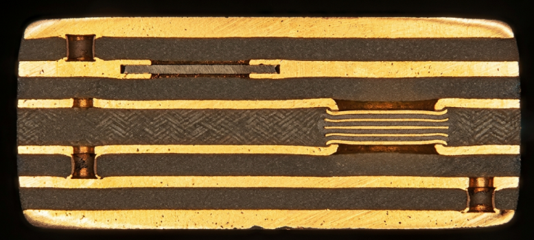
The process for producing PCBs with embedded passives is more than a typical multilayer process. In the case of thin-film resistors, the starting point is a copper-clad core with a resistive alloy (e.g., NiP) layer bonded to it:
- Use photolithography to pattern the resistor shape on the resistive layer.
- Etch away copper to form the circuit pattern, leaving the resistive elements.
- Protect resistive elements with a coating.
- Laminate with prepreg and other layers.
- Laser-trim resistors for improved tolerances if required.
Embedded capacitors also start with laminating a thin capacitive laminate (dielectric thickness 4-24 micrometers) between copper layers, and then patterning the copper to form the plates. The cavity embedding process differs in that it involves carving a cavity into the substrate, inserting a factory-trimmed discrete component into the cavity, and then covering it with resin before laminating the next layer.
Advanced Testing for Zero Defects and High Yield
The inability to visually inspect embedded components after lamination is the biggest challenge. Manufacturers rely on specialized strategies:
- In-process resistance testing: Resistors are tested after etching but before lamination, the final opportunity for laser trimming.
- LCR testing: Embedded capacitors are tested at designated frequencies (usually 1 MHz) for capacitance and dissipation factor.
- Time Domain Reflectometry (TDR): Checks for impedance continuity and imperfections that may cause signal reflection.
- Cross-section: Destructive evaluation of panel coupons to confirm layer alignment, dielectric thickness, and element integrity.
- X-rays: Non-destructive screening for cavity-embedded discrete components.
These procedures comply with IPC-6012 Class 3 qualification for rigid PCBs for high-reliability applications.
JLCPCB's Expertise in Embedded Passive Component PCBs
Advanced PCB and Packaging Capabilities
Embedded passive component PCBs require a manufacturer with cutting-edge process technology and quality control. JLCPCB offers support for all types of embedding, whether it be thin-film embedded resistors, high-Dk embedded capacitors, or cavity-embedded components.
The production facilities have laser drilling for microvias down to 75 micrometers and depth-controlled routing for cavity formation to support the tight tolerances required for embedded passives. From a 6-layer HDI board with embedded decoupling to a 10-layer RF board with embedded termination resistors, their engineers help specify a stackup. JLCPCB's DFM review points out any issues with your embedded passive design, such as a lack of clearance, unrealistic tolerance requirements, and layer registration issues with capacitor plate alignment. Their real-time quoting engine supports the extra process steps, allowing you to get cost information to inform your cost-benefit analysis during the design phase.
Proven Reliability for High-Density and High-Performance Boards
JLCPCB's quality system meets IPC-6012 and IPC-A-600 Class 2 and Class 3 requirements, delivering traceability and process control required for automotive, aerospace, medical, and telecommunication applications. JLCPCB provides extra in-process checks on boards with embedded passives, in addition to electrical testing. If you are considering using an embedded passive technology for your next design, you can upload the Gerber files and receive an instant quote to determine if the technology is right for your project.
Frequently Asked Questions (FAQ)
Q: What types of passive components can be embedded inside a PCB?
Resistors, capacitors, and inductors. Embedded resistors use thin-film alloys like nickel-phosphorus on internal copper layers. Embedded capacitors use high-permittivity dielectric layers between planes. Embedded inductors use spiral traces on internal layers for low-value RF applications.
Q: What tolerance can I expect from embedded passive components?
Embedded resistors achieve plus or minus 5 to 10 percent without laser trimming, and plus or minus 1 percent with trimming. Embedded capacitors hold plus or minus 10 to 20 percent. Design your circuit to accommodate these ranges or specify trimming where accuracy is critical.
Q: Are embedded passives more expensive than surface-mount components?
Per-board fabrication cost is higher, but total system cost can drop at medium to high volumes because you reduce assembly steps, eliminate solder joints, and achieve smaller board sizes with better panel yield.
Q: Are embedded passives more expensive than surface-mount components?
Per-board fabrication cost is higher, but total system cost can drop at medium to high volumes because you reduce assembly steps, eliminate solder joints, and achieve smaller board sizes with better panel yield.
Q: When should I choose embedded passives over surface-mount parts?
When board space is severely constrained, high-frequency performance demands minimal parasitics (above 1 GHz), or reliability requirements call for eliminating solder joints. They are ideal for decoupling capacitors, termination resistors, and RF matching networks.
Q: Do embedded passives affect the PCB stackup design?
Yes, significantly. You must allocate specific internal layers for embedded elements during stackup planning. This must be defined from the beginning of the design process, not added as an afterthought.
Conclusion
Embedded passive components represent a significant leap forward in PCB design, enabling engineers to create smaller, faster, and more reliable electronic products. By embedding resistors, capacitors, and inductors within the board layers, designers can dramatically reduce board size, minimize parasitic effects, improve signal integrity, and enhance overall product reliability — all while lowering long-term assembly costs.
As consumer electronics, 5G devices, automotive radar, and high-frequency applications continue to demand more compact and high-performance solutions, embedded passives are no longer a niche technology but a competitive necessity.
Ready to unlock smaller and smarter PCBs for your next project? JLCPCB offers advanced embedded passive capabilities, expert DFM support, and reliable manufacturing to bring your innovative designs to reality. Upload your Gerber files today and experience the future of PCB technology.
Keep Learning
Your Ultimate Guide to PCB Rulers
In the world of PCB design and manufacturing, having the right tools is crucial for achieving accuracy and precision. One such tool that has gained popularity among professionals and hobbyists is the PCB ruler. This specialized measuring tool is designed to provide accurate measurements, reference information, and component footprints, assisting designers, engineers, technicians, and assemblers in various stages of PCB development. In this guide, we'll explore what a PCB ruler is, the features and mea......
How Laser Drilling Delivers Precision and Density in Advanced PCB Manufacturing
Key Takeaways Laser Drilling has become the cornerstone technology for precision and high-density PCB manufacturing, enabling microvias as small as 25-75μm — far beyond the 150μm limit of mechanical drilling. By delivering superior accuracy, contactless processing, excellent signal integrity, and reliable blind/stacked vias, it empowers advanced HDI board designs essential for modern electronics. From optimal stackup selection to professional plating and DFM practices, mastering laser drilling is key ......
Unlocking Smaller, Smarter PCBs with Embedded Passive Components
Key Takeaways Embedded passive components are revolutionizing PCB design by integrating resistors, capacitors, and inductors directly into the board layers. This technology delivers smaller, thinner, and higher-performance boards with up to 30-50% space savings, significantly reduced parasitic inductance, superior signal integrity at high frequencies, better thermal distribution, and enhanced reliability through fewer solder joints. Ideal for 5G, wearable, automotive, and RF applications, embedded pas......
Reducing CTE Mismatch Stress: Practical Ways to Build More Reliable PCBs
Key Takeaways CTE mismatch (FR4’s high Z‑axis CTE vs. copper) creates thermal stress that causes PCB warpage, via cracks, delamination, and solder fatigue—worse under lead‑free reflow and thermal cycling. Mitigate it with symmetric stackups and balanced copper, higher‑Tg/low‑CTE materials, and tight process control (lamination, cooling, moisture, and consistent via plating). Are you aware that the coefficient of thermal expansion of standard FR4 in the Z-axis can be up to 70 ppm/C, whereas copper has ......
Why UL94 V0 Matters for Safe and Reliable PCB Manufacturing
Key Takeaways UL94 V0 is the highest flame rating for PCB materials, requiring self-extinguishing within 10 seconds with no flaming drips. It greatly reduces fire risk and has become the de facto standard for safe, reliable PCBs in consumer, industrial, automotive, and medical applications. JLCPCB offers UL94 V0 compliant FR4 and high-Tg materials by default, ensuring regulatory compliance (UL, CE, CCC) and long-term reliability without compromising performance or budget. Never sacrifice V0 rating for......
How to Choose the Right UL94 Rating for Safe and Reliable PCBs
Key Takeaways This article explains how to choose the right UL94 rating to ensure PCB fire safety and compliance: V-0 is the common baseline for most electronics, V-1/HB are typically for lower-risk or non-regulated uses. It also stresses that rating performance depends on material selection, thickness, and process control, so use UL-certified laminates and a traceable, UL-capable manufacturer. Have you heard that just one PCB that catches fire can produce poisonous fumes, annihilate an entire product......