
TQFP Package Explained: Dimensions, Pin Pitch, PCB Design & Comparisons
12 min
- What Is a TQFP Package?
- TQFP Package Structure and Key Characteristics Explained
- TQFP Package Dimensions and Pin Pitch
- TQFP vs Standard QFP
- TQFP vs LQFP
- TQFP vs QFN: Which Package Should You Choose?
- PCB Footprint Design Guidelines for TQFP Packages
- TQFP Soldering and Assembly Considerations
- Advantages and Disadvantages of TQFP Packages
- Typical Applications of TQFP Package
- Is the TQFP Package Still Relevant Today?
- FAQs
- Conclusion
The constant push for miniaturization in modern electronics demands highly efficient PCB layouts. As surface-mount technology (SMT) has evolved, engineers have constantly sought component packages that balance high pin density with manufacturability. For mid-to-high I/O density applications where the extreme routing complexity and X-ray inspection requirements of a BGA (Ball Grid Array) are unnecessary, the TQFP package remains an industry-standard go-to.
This guide explores everything you need to know about designing, routing, and assembling TQFP components.
What Is a TQFP Package?
If you are a hardware engineer, you might ask, what is TQFP package technology, and why is it so prevalent in microcontrollers? TQFP stands for thin quad flat package. It is a surface-mount integrated circuit (IC) package characterized by its square or rectangular body with leads extending outward from all four sides.
The defining technical hallmark of the TQFP is its exceptionally low profile. With a standard body thickness of just 1.0 mm, it is designed specifically to meet the strict height constraints of modern electronics without sacrificing pin count or ease of assembly.
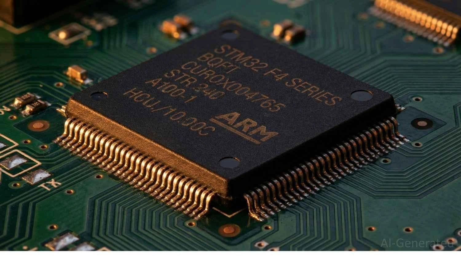
Figure: Close-up view of a Thin Quad Flat Package (TQFP) microcontroller showing pins on all four sides.
TQFP Package Structure and Key Characteristics Explained
Body thickness and lead frame design
The TQFP utilizes a plastic molded body enveloping a copper lead frame. While traditional flat packages can be bulky, the TQFP strictly adheres to a 1.0 mm nominal body thickness. This ultra-thin resin compound provides adequate protection for the internal silicon die and wire bonds while keeping the overall volume minimal.
Gull-wing leads explained
The leads extending from the TQFP package are bent into a "gull-wing" shape. This mechanical design is crucial; the gull-wing leads act as tiny shock absorbers. During thermal cycling (when the PCB and IC expand and contract at different rates) or mechanical board flexure, these leads flex slightly, preventing the solder joints from cracking.
Why “thin” matters in PCB stacking
In modern space-constrained devices - such as IoT sensors, tablets, and slim consumer electronics - vertical Z-axis space is just as valuable as horizontal X-Y space. The 1.0 mm thickness allows engineers to stack PCBs closer together or fit complex logic boards into ultra-slim enclosures. If you are working on tight-fitting designs, optimizing component height is just as critical as routing, which is especially true in compact applications like wearable PCB assembly.
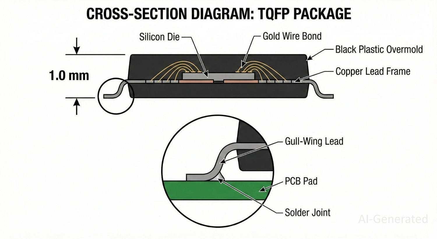
Figure: TQFP package body thickness and gull-wing lead structure.
TQFP Package Dimensions and Pin Pitch
Common pin counts (64 / 100 / 144 / 176 / 208)
TQFP packages are highly scalable. For simpler peripheral ICs, they may start at 32 or 44 pins. However, they are most famous for housing high-performance microcontrollers and FPGAs, commonly featuring 64, 100, 144, 176, or even 208 pins.
Standard pin pitch options (0.8mm / 0.65mm / 0.5mm)
The "pitch" is the distance from the exact center of one pin to the center of the adjacent pin. TQFPs typically come in pitches of 0.8mm, 0.65mm, 0.5mm, and occasionally 0.4mm. As the pitch decreases, manufacturing difficulty increases. A 0.5mm or 0.4mm pitch requires extremely strict solder paste volume control and highly precise stencil alignment to prevent bridging during reflow.
TQFP package size chart
While general sizes are standardized, engineers must always consult the specific IC’s tqfp datasheet to confirm exact pad geometries before designing footprints. Below is a reference chart for common TQFP package dimensions:
| Pin Count | Body Size (mm) | Standard Pitch (mm) |
|---|---|---|
| 32 / 44 | 10 × 10 | 0.80 |
| 64 | 10 × 10 | 0.50 |
| 100 | 14 × 14 | 0.50 |
| 144 | 20 × 20 | 0.50 |
| 176 | 24 × 24 | 0.50 |
TQFP vs Standard QFP
What’s the difference between the TQFP package and the standard QFP?
When evaluating TQFP vs. QFP, the primary differentiator is the Z-axis profile. Standard Quad Flat Packages (QFP) typically have a body thickness ranging from 2.0 mm to 3.8 mm, making them significantly bulkier. TQFP strictly maintains a 1.0 mm thickness.
TQFP vs QFP Applications: When to Choose Each Package Type
Standard QFPs are often found in legacy designs or high-power applications where a thicker molding compound is used for specific thermal or robust mechanical requirements. However, for almost all modern, height-constrained designs, TQFP is the superior choice over standard Quad Flat Package variants.
TQFP vs LQFP
What’s the difference between the TQFP package and the LQFP package?
The distinction in TQFP vs LQFP also comes down to body thickness. LQFP (Low-profile Quad Flat Package) sits precisely between standard QFP and TQFP, featuring a body thickness of 1.4 mm. TQFP remains thinner at 1.0 mm.
TQFP vs LQFP: When to Choose Each Package Type
The choice between the two usually depends on IC availability rather than design preference, as many silicon vendors default to LQFP for standard MCUs, making the TQFP vs LQFP debate largely a matter of supply chain logistics.
TQFP vs QFN: Which Package Should You Choose?
The debate of TQFP vs. QFN (Quad Flat No-leads) is incredibly common among PCB designers. Here is how they stack up:
● Assembly difficulty: TQFP is generally easier for visual inspection because the leads are exposed. QFNs have pads underneath the package, making them prone to solder voiding on the center thermal pad if the paste stencil isn't perfectly designed.
● PCB routing space: QFN is the clear winner for miniaturization, as it saves significant board space by eliminating extended leads. TQFPs require a larger overall footprint.
● Thermal performance: QFNs excel thermally due to their large exposed center die-attach pad, which solders directly to the PCB ground plane for heat dissipation.
● Rework and inspection: TQFP is highly reworkable. An engineer can easily replace a TQFP chip using a basic hot air gun, tweezers, and a soldering iron. QFN rework is much more difficult without specialized hot-air stations.
Regardless of the package you choose, sourcing authentic ICs through a reliable component platform like JLCPCB parts is the best way to prevent unexpected assembly defects and ensure long-term reliability.
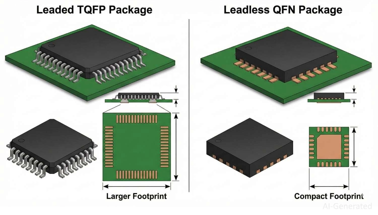
Figure: Side-by-side comparison illustrating the physical footprint differences between leaded TQFP and leadless QFN packaging.
PCB Footprint Design Guidelines for TQFP Packages
Land pattern basics
Creating an accurate TQFP footprint is essential for a reliable solder joint. Designers should strictly follow IPC-7351 standard recommendations. This ensures appropriate heel fillets (the solder joint on the inside of the bend), toe fillets (on the tip of the lead), and side fillets. If the toe fillet is ignored, the mechanical strength of the joint drops significantly.
Solder mask and paste opening tips
For fine-pitch TQFPs (0.5mm and below), solder mask expansion must be tightly controlled. It is critical to maintain a "solder mask dam" (usually a minimum of 0.075mm to 0.1mm) between adjacent pads. If the dam is too thin, the PCB manufacturer may remove it entirely, drastically increasing the risk of solder bridging - a critical factor often highlighted in advanced solder pad design guidelines.
Common footprint mistakes to avoid
The most common mistakes include mismatched pin pitches, incorrectly sized toe radii, and failing to account for the overall package tolerance. Always verify the footprint against the manufacturer’s recommended land pattern rather than relying entirely on generic CAD library footprints.
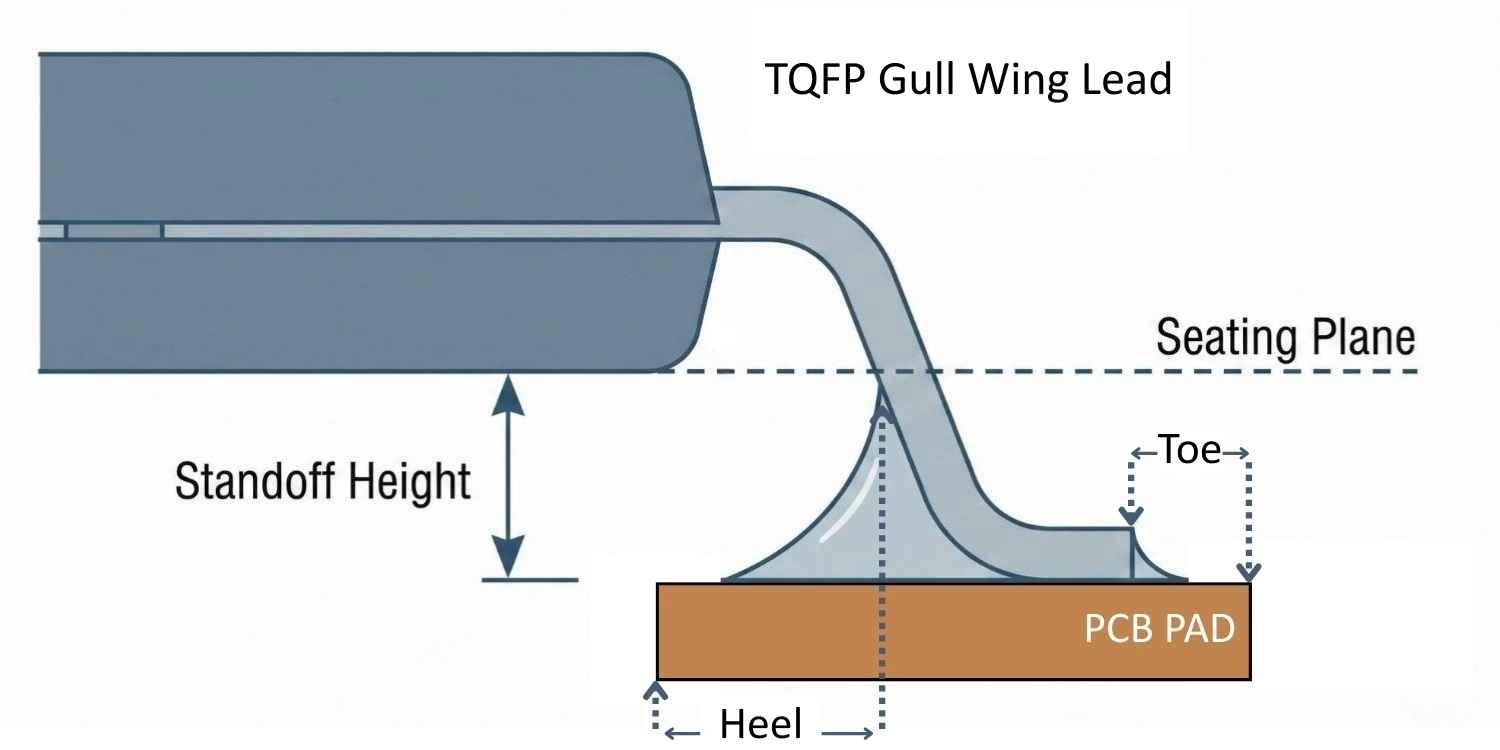
Figure: PCB footprint diagram showing proper heel, toe, and side fillet dimensions for a TQFP land pattern.
TQFP Soldering and Assembly Considerations
Reflow soldering suitability
TQFP packages are perfectly suited for standard reflow soldering. However, because the package is thin and the leads are numerous, coplanarity is critical. If the leads are bent during handling and don't sit perfectly flat on the PCB pads, standard reflow profiles will result in open circuits (unconnected pins).
Tombstoning & bridging risks
While tombstoning (where a component stands up on one end) is a common issue for small passive components like 0402 resistors, it is practically non-existent for heavy, multi-pin TQFPs. Instead, the number one defect during TQFP soldering is bridging - where solder paste melts and connects two adjacent pins. This is mitigated by using correct stencil thickness (typically 0.1mm to 0.12mm for fine pitch) and high-quality solder paste.
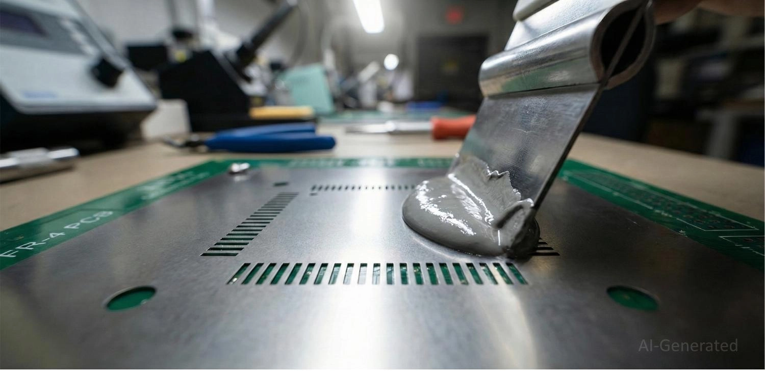
Figure: Macro view of a solder paste stencil applied over a fine-pitch TQFP PCB footprint to prevent bridging.
AOI and X-ray inspection relevance
Because all pins are visible on the exterior, Automated Optical Inspection (AOI) machines can easily catch bent leads, insufficient solder, or solder bridges on a TQFP. Unlike BGAs, X-ray inspection is generally not required for TQFP unless there are hidden ground pads.
Professional PCB assembly providers typically combine stencil optimization, AOI inspection, and controlled reflow profiling to ensure high-yield TQFP assembly. JLCPCB’s PCB assembly service integrates automated inspection and precision SMT processes specifically optimized for fine-pitch packages like TQFP.

Advantages and Disadvantages of TQFP Packages
Advantages of the TQFP Package
● Inspectability: Solder joints can be visually inspected with the naked eye or standard microscopes.
● Maturity: The manufacturing and assembly processes are highly mature, resulting in excellent yields.
● Testing & Programming: An off-the-shelf TQFP socket can be easily sourced. Engineers can pop the chip into a socket for initial firmware flashing or testing before permanently soldering it to the board.
● Reworkability: Easy to desolder and replace by hand during prototyping.
Limitations of the TQFP Package
● Board Space: They consume a massive amount of X-Y real estate compared to QFN or BGA packages.
● I/O Density Limit: Usually capped at around 208 pins. Designs requiring more I/O must transition to BGAs.
● Fragility: The long, thin, exposed copper leads are highly vulnerable to bending if dropped or handled roughly prior to assembly.
Typical Applications of TQFP Package
Because of their balance of pin count and assembly ease, TQFPs are ubiquitous. You will find them heavily used in:
● Microcontrollers (MCUs): The vast majority of 32-bit MCUs, such as the STM32, PIC32, and ATMega series, utilize TQFP packaging.
● Industrial control boards: Where mechanical reliability and ease of inspection trump the need for extreme miniaturization.
● Consumer electronics: Inside home appliances, motor controllers, and audio equipment.
● Legacy-to-mid-range designs: Acting as reliable interfaces, logic gates, or motor drivers.
Is the TQFP Package Still Relevant Today?
With the rise of ultra-dense BGAs (Ball Grid Arrays) and CSPs (Chip Scale Packages), one might wonder if TQFP is obsolete. The answer is a resounding no.
Engineers still heavily prefer TQFP for rapid prototyping and lower-layer-count PCBs (like 2-layer or 4-layer boards), as routing escape traces from a TQFP does not require expensive microvias as a BGA does. Furthermore, in environments subject to severe mechanical shock or vibration, the gull-wing leads of a TQFP can survive stresses that would easily shear the rigid solder balls of a BGA.
As long as there is a need for accessible, easily inspectable, mid-density I/O routing, the TQFP will remain a staple in hardware design.
FAQs
Q: What does TQFP stand for?
TQFP stands for Thin Quad Flat Package. It is a specific type of SMT package that restricts body thickness to 1.0 mm to support low-profile electronic designs.
Q: What is the smallest pin pitch of TQFP?
While 0.8mm and 0.5mm are the most common, the smallest standard pitch for TQFP packages is typically 0.4mm. Assembling 0.4mm pitch components requires high-precision stencil printing to avoid solder bridges.
Q: Is TQFP easy to solder by hand?
Yes, relatively speaking. Using a technique called "drag soldering" alongside a generous application of high-quality flux, an experienced engineer can easily solder fine-pitch TQFPs by hand during the prototyping phase.
Q: Can TQFP be used for high-speed designs?
Up to a certain frequency, yes. However, because of the physical length of the internal bond wires and external gull-wing leads, TQFPs introduce parasitic inductance and capacitance. For ultra-high-speed RF or gigabit digital designs, leadless packages (like QFN) or BGAs are preferred due to their shorter electrical paths.
Q: How do you remove or rework a TQFP component from a PCB?
To safely remove a TQFP, engineers typically use a hot air rework station. By applying generous amounts of flux to the pins and evenly heating all four sides of the IC simultaneously using a square-shaped hot air nozzle, the solder melts, allowing the chip to be easily lifted away with vacuum tweezers.
Q: Does a standard TQFP package have an exposed thermal pad?
Standard TQFPs do not have an exposed thermal pad on the bottom; they rely entirely on the internal lead frame and the plastic body to dissipate heat. However, there is a specialized high-power variant called HTQFP (Thermally Enhanced TQFP), which includes an exposed die-attach pad on the bottom that is meant to be soldered directly to the PCB ground plane.
Conclusion
The tqfp package continues to strike a perfect balance between high pin density, low vertical profile, and high manufacturing yield. By understanding its specific dimensions, pitch constraints, and proper footprint design rules, engineers can ensure flawless assembly and reliable product performance.
Ready to build your next design? Trust a PCB manufacturer that understands the details. Get an instant quote for your PCB Assembly at JLCPCB and experience the difference high-precision manufacturing makes.

Popular Articles
• SMD Capacitor Sizes: Complete Size Chart and Selection Tips for PCB Design and Assembly
• SMD Diode Code Lookup: Full List, Marking Guide & Identification [2026 Guide]
• SMD Resistor Package Sizes: Complete Size Chart, Footprints & How to Choose
• SMD Capacitor Codes: Identification, Markings, and Polarity
• How to Solder SMD Components Like a Pro [2026 Updated]
Keep Learning
SMD Transistor Code Lookup: Identify Markings, Pinout & Multimeter Test Guide
Repairing a circuit board often brings a familiar frustration: staring at a tiny, three-legged black component with an obscure two- or three-letter code. Whether troubleshooting a bare prototype or a mass-produced PCBA, knowing how to quickly decode these surface-mount device (SMD) markings is an essential skill for any electronics engineer or repair technician. In this comprehensive guide, you will learn: 1. How to decode SMD transistor marking codes 2. How to identify BJT vs MOSFET types 3. How to f......
SMD Capacitor Sizes: Complete Size Chart and Selection Tips for PCB Design and Assembly
In the world of modern electronics, surface mount devices (SMDs) have revolutionized board design, allowing for smaller, faster, and more efficient printed circuit boards. When designing a PCB, selecting the correct SMD capacitor sizes is one of the most critical decisions an engineer must make to ensure both electrical reliability and manufacturability. In this article, you will find practical, authoritative guidance on: Comprehensive SMD capacitor size charts for quick reference. How to read imperia......
SMD Diode Code Lookup: Full List, Marking Guide & Identification [2026 Guide]
In modern electronics, surface-mount diodes are used everywhere - from power input protection circuits to high-speed signal routing. Because these components are extremely small, manufacturers cannot print full part numbers on their bodies. Instead, they use short marking codes such as A2, M7, SS14, or SL, which often confuse beginners during PCB repair, reverse engineering, or component replacement. This guide explains how to decode SMD diode codes, identify polarity, test components using a multimet......
Thin Film vs. Thick Film Resistors: Key Differences & Selection Guide
Key Takeaways Default to thick film resistors for most designs. They are cost-effective, robust, and ideal for pull-ups, LED current-limiting, digital circuits, and surge-prone applications. Choose thin-film resistors whenever a resistor defines an analog quantity, such as a voltage divider, reference network, gain-setting circuit, or current-sensing signal chain. Their tight tolerance and low TCR help maintain measurement accuracy over temperature and time. Most PCB designs use thick film or thin fil......
Capacitor Types Explained: Applications, Differences, and Selection Guide
Capacitors are the most widely used parts in electronics design, from input/output coupling to bypassing and decoupling networks; they find applications everywhere. And if you get the wrong part/value placed, the consequences may be you get an audible whine from a supply rail, a bootloader that won't start, or a capacitor that lights up like a match. The question that never comes up is "which brand?" It's always “which type and what value.” This tutorial does not waste time on a textbook explanation o......
PoP Package (Package on Package) Explained: Architecture, Assembly, and SMT Challenges
In the race for miniaturization, fitting more processing power into smaller footprints is the ultimate challenge for PCB designers. Package on Package (PoP) technology answers this by integrating logic and memory vertically, becoming the standard for modern mobile processors. However, this 3D architecture demands advanced SMT assembly capabilities beyond standard fabrication. JLCPCB specializes in the high-precision manufacturing required to master these complex stacks. This guide covers how PoP packa......