
QFP vs QFN: Which IC Package Is Right for Your PCB?
12 min
- What Is QFP Package?
- What Is QFN Package?
- QFP vs QFN: Quick Selection Guide
- QFP vs QFN: Key Differences at a Glance
- QFP vs QFN: Application Scenarios: When to Choose Which
- QFP vs QFN: PCB Footprint & Design Considerations
- QFP vs QFN: Soldering and Assembly Challenges
- How JLCPCB Supports Your QFP and QFN Projects
- Advantages of QFP Package
- Limitations of QFP Package
- Advantages of QFN Package
- Limitations of QFN Package
- FAQ
- Conclusion: Choosing Between QFP and QFN
QFP and QFN are two widely used IC packages in modern PCB design, each offering different advantages in size, assembly, and performance. Choosing between QFP vs QFN directly impacts layout complexity, soldering reliability, thermal management, and manufacturing cost.
An improper package selection may lead to low production yield, higher rework rates, and long-term reliability issues. In this guide, we compare QFP and QFN in terms of structure, PCB footprint, assembly process, and typical applications, helping engineers and designers make informed decisions for their projects.
What Is QFP Package?
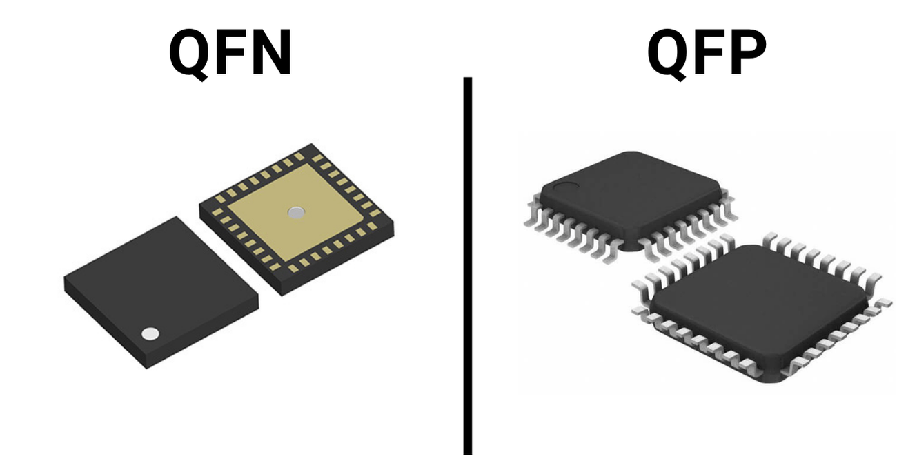
QFP stands for Quad Flat Package, a surface-mount IC package with gull-wing leads extending from all four sides. It is designed to support medium to high pin counts while maintaining reliable electrical and mechanical performance.
QFP packages are widely used in microcontrollers, interface chips, and embedded processors due to their mature manufacturing process and broad industry support.
Typical pin counts range from 44 to over 200 pins, while common pin pitches include 0.8 mm, 0.65 mm, and 0.5 mm. These standardized dimensions make QFP components compatible with most PCB fabrication and assembly processes.
What Is QFN Package?
QFN stands for Quad Flat No-Lead, a surface-mount IC package that features flat metal pads on the bottom instead of extended leads. These pads are directly soldered to the PCB, allowing the package to achieve a smaller footprint and lower profile than traditional leaded packages.
Most QFN packages also include a central exposed thermal pad, which helps transfer heat from the chip to the PCB. This structure improves thermal and electrical performance, making QFN popular in high-speed and high-power applications.
Typical QFN pin counts range from 16 to over 100 pins, with common pitches of 0.5 mm and below. Due to their compact size and excellent electrical characteristics, QFN packages are widely used in wireless modules, power management ICs, and high-frequency devices.
QFP vs QFN: Quick Selection Guide
If you need to choose quickly between QFP and QFN packages, the table below summarizes the most practical decision factors.
| Requirement | Recommended Package | Reason |
|---|---|---|
| Easy Rework & Debugging | QFP | Leads are visible and accessible for soldering and probing |
| Small PCB Size | QFN | No external leads, smaller footprint |
| High-Frequency Performance | QFN | Lower parasitics and shorter signal paths |
| Rapid Prototyping | QFP | Easier hand soldering and modification |
| Mass Production | QFN | Better suitability for automated assembly |
| Thermal Performance | QFN | Exposed pad improves heat dissipation |
| Visual Inspection | QFP | Solder joints are easy to inspect |
Engineer's Tip: If your design is still in the validation or iteration stage, starting with QFP can significantly reduce development time. Once the design is mature and stable, migrating to QFN is often the best path for size reduction and performance optimization.
QFP vs QFN: Key Differences at a Glance
Choosing between QFP and QFN requires a clear understanding of their structural, electrical, and manufacturing differences. Although both packages are widely used in PCB design, they serve different application needs.
The table below summarizes the key differences between QFP and QFN packages.
QFP vs QFN Comparison Table
| Feature | QFP (Quad Flat Package) | QFN (Quad Flat No-Lead) |
|---|---|---|
| Lead Type | Gull-wing leads | Bottom pads (no leads) |
| PCB Footprint | Larger | Smaller |
| Pin Density | Moderate | High |
| Assembly Difficulty | Lower | Higher |
| Thermal Performance | Moderate | Better |
| Inspection Method | Visual / AOI | X-ray / Advanced AOI |
| Reworkability | Easy | Difficult |
| Signal Integrity | Good | Better |
| Manufacturing Yield | Stable | Process-dependent |
1. QFP vs QFN: Structural Differences
The main difference between QFP and QFN lies in their lead structure.
QFP Structure
● Uses external gull-wing leads
● Leads extend from all four sides
● Solder joints are visible and accessible
● Easy to inspect and rework
QFN Structure
● Uses bottom pads with no external leads
● Pads are located underneath the package
● Smaller package size
● Better electrical performance
● Inspection and rework are more difficult
Key takeaway: QFP focuses on accessibility and ease of repair, while QFN focuses on compactness and performance.
2. QFP vs QFN: PCB Layout and Routing Impact
Package selection directly affects PCB routing complexity.
QFP Layout Characteristics
● Requires more board space
● Larger footprint
● Easier fan-out routing
● Suitable for low-layer PCBs
QFN Layout Characteristics
● Enables compact board design
● Requires precise pad layout
● Needs careful via and thermal pad design
● Higher risk of layout-related defects
Common Risk: Poor QFN routing may lead to soldering failures and thermal problems.
Design tip: Choose QFP for simpler layouts and QFN for space-critical designs with strong DFM support.
3. QFP vs QFN: Thermal and Electrical Performance Comparison
Thermal and electrical behavior is a major decision factor.
Thermal Performance
QFN
● Exposed center thermal pad
● Efficient heat transfer
● Lower junction temperature
● Better for power devices
QFP
● No central thermal pad
● Moderate heat dissipation
● Higher thermal resistance
Electrical Performance
QFN
● Short signal paths
● Lower parasitic inductance
● Better for high-frequency circuits
QFP
● Longer leads
● Higher parasitic effects
● Less suitable for very high-speed designs
Key takeaway: QFN is superior for thermal and high-speed applications.
4. QFP vs QFN: Manufacturing and Cost Considerations
Manufacturing complexity has a direct impact on cost and yield.
QFP Manufacturing Features
● Mature assembly process
● Easy visual inspection
● High and stable yield
● Low rework cost
● Suitable for prototypes and small batches
QFN Manufacturing Features
● Requires precise stencil design
● Needs accurate placement
● Sensitive to reflow profile
● Often requires X-ray inspection
● Higher process control requirement
Cost Perspective
| Production Type | Recommended Package |
|---|---|
| Prototyping | QFP |
| Low–Medium Volume | QFP |
| High Volume (Advanced Line) | QFN |
Cost tip: QFN can be cost-effective in mass production, but QFP is usually safer for early-stage projects.
QFP vs QFN: Application Scenarios: When to Choose Which
Both QFP and QFN packages are widely used across different industries, but their structural differences make them better suited for specific applications. The table below summarizes typical use cases:
| Application Area | QFP (Quad Flat Package) | QFN (Quad Flat No-Lead) |
|---|---|---|
| Microcontrollers (MCUs) | Widely used, easy rework | Less common, compact designs preferred |
| DSPs & Communication ICs | Suitable for prototyping | High-frequency or compact modules |
| Consumer Electronics | Medium-density boards | Space-constrained devices like smartphones & wearables |
| Industrial Control | Stable, easy inspection | Compact, thermal-efficient boards |
| Power Management ICs | Moderate heat dissipation | Excellent thermal performance |
| Embedded Systems | Prototyping & small batch | High-density, performance-critical designs |
Key Takeaway:
● QFP is preferred for projects where ease of inspection, rework, and prototyping are priorities.
● QFN is ideal for space-constrained, high-performance boards requiring precise soldering and thermal efficiency.
QFP vs QFN: PCB Footprint & Design Considerations
Proper footprint design is critical for achieving reliable soldering and stable manufacturing when using QFP or QFN packages.
QFP Footprint Guidelines
● Use standard IPC land patterns
● Ensure sufficient solder mask clearance
● Allow space for easy probe access and rework
● Keep uniform pad spacing to prevent bridging
Best for: Beginners, prototypes, and low-risk designs
QFN Footprint Guidelines
● Design accurate pad and thermal pad sizes
● Optimize solder paste aperture ratio
● Consider via-in-pad for heat dissipation
● Balance thermal and electrical performance
Best for: Compact and high-performance boards
Common PCB Design Mistakes to Avoid
● Oversized or undersized pads
● Poor thermal pad connection (QFN)
● Incorrect solder paste coverage
● Ignoring manufacturer land pattern data
Design tip: Always verify footprints with DFM checks before fabrication to reduce assembly defects and improve production yield.
QFP vs QFN: Soldering and Assembly Challenges
Soldering is a key consideration when choosing between QFP and QFN packages, as each has unique challenges that can affect manufacturing yield and reliability.
QFP Soldering Tips
● Use proper reflow profiles to avoid cold joints
● Gull-wing leads allow visual inspection and easy touch-up
● Tombstoning is rare due to lead visibility
● Suitable for prototyping and small-to-medium batch assembly
Key advantage: Easier inspection and rework compared to leadless packages
QFN Soldering Tips
● Ensure accurate stencil design for thermal and signal pads
● Use controlled reflow profiles to avoid voiding
● Solder joints are hidden under the package, requiring X-ray or advanced AOI inspection
● Higher precision needed for placement and solder paste volume
Key challenge: Harder to inspect and rework, but allows smaller footprints and better thermal/electrical performance
Best Practices for Both Packages
● Verify reflow temperature profiles with manufacturer specs
● Check pad alignment and solder paste coverage before assembly
● Consider automated inspection (AOI/X-ray) for QFN
● Use prototypes to validate soldering process before mass production
How JLCPCB Supports Your QFP and QFN Projects
When bringing your QFP or QFN-based PCB to life, choosing the right manufacturer is crucial.
At JLCPCB, we provide fast-turn prototyping so you can test and iterate your designs in as little as 24–48 hours—ideal for QFP components that require easy rework.
Our advanced SMT and PCBA services meet the precision demands of QFN soldering, including X-ray inspection and AOI checks to ensure every joint is reliable.
With a global logistics network, JLCPCB delivers your boards quickly, helping you meet tight deadlines without compromising quality.

Advantages of QFP Package
1. Easy to Inspect & Rework
One major advantage of QFP packages is their exposed leads, which allow easy visual inspection using AOI systems or manual checking. Defective solder joints can be quickly identified and repaired, making QFP suitable for prototyping and low-to-medium volume production.
Rework and replacement are also simpler compared to leadless packages, reducing maintenance cost and downtime.
2. Standardized Process
QFP packages follow well-established industry standards for footprint design, soldering profiles, and inspection methods. Most PCB manufacturers and assembly providers are highly experienced in handling QFP components, ensuring stable production quality and consistent yield.
This standardization reduces manufacturing risks and shortens product development cycles.
Limitations of QFP Package
1. Larger Footprint
Compared with modern compact packages, QFP requires more PCB surface area due to its extended leads. This larger footprint limits its use in size-constrained products such as wearable devices and ultra-compact modules.
2. Lower Pin Density
Although QFP supports relatively high pin counts, its pin density is lower than that of QFN or BGA packages. As pin pitch decreases, routing becomes more difficult and increases the risk of solder bridging, which may affect production yield.
This makes QFP less suitable for high-density and high-performance designs.
Advantages of QFN Package
1. Smaller Footprint and Higher Pin Density
One of the main advantages of QFN packages is their compact design. Without external leads, QFN occupies significantly less PCB area than QFP, allowing designers to place more components on the same board.
This higher pin density is especially beneficial for miniaturized products such as IoT devices, smartphones, and portable electronics.
2. Better Thermal and Electrical Performance
The exposed thermal pad in QFN packages provides an efficient heat dissipation path, reducing junction temperature and improving long-term reliability.
In addition, the short electrical path between the chip and PCB lowers parasitic inductance and resistance. This results in better signal integrity, making QFN suitable for high-frequency and high-speed circuits.
Limitations of QFN Package
1. Difficult Inspection and Rework
Because QFN solder joints are located underneath the package, visual inspection is difficult using standard optical methods. Advanced inspection techniques such as X-ray inspection are often required to detect voids, bridges, or insufficient solder.
Reworking QFN components is also more challenging and usually requires specialized equipment and experienced technicians.
2. Higher Assembly Precision Requirement
QFN assembly demands precise solder paste printing, accurate placement, and well-controlled reflow profiles. Improper stencil design or thermal profiling may lead to defects such as solder voiding, poor wetting, or insufficient bonding.
As a result, QFN packages require higher process control and manufacturing expertise compared to QFP.
FAQ
Q1: Is QFN better than QFP?
It depends on your design priorities. QFN packages offer a smaller footprint, higher pin density, and better thermal and electrical performance, making them ideal for compact and high-speed boards. QFP packages, on the other hand, are easier to inspect and rework, which is advantageous for prototypes and low-to-medium volume production.
Q2: Can QFP be reworked easily?
Yes. QFP packages have exposed gull-wing leads that make visual inspection, solder touch-up, and replacement straightforward. This rework-friendly nature is one of the main reasons QFP remains popular in prototyping and boards where easy maintenance is required.
Q3: Does QFN require X-ray inspection?
Often, yes. QFN solder joints are located under the package, making visual inspection difficult. To ensure solder quality and detect voids or bridges, X-ray inspection or advanced AOI systems are typically used, especially for high-reliability applications.
Q4: Which is cheaper: QFP or QFN?
The cost depends on production volume and assembly complexity. QFP usually has lower manufacturing complexity, making it more cost-effective for prototypes and small batches. QFN can be competitive for high-volume production but requires stricter process control and inspection, which may increase assembly costs.
Conclusion: Choosing Between QFP and QFN
Selecting the right package—QFP vs QFN—depends on your project needs. QFP is ideal for prototypes and designs requiring easy inspection and rework, while QFN excels in compact, high-performance boards with better thermal and electrical characteristics.
At JLCPCB, we support both QFP and QFN projects with fast-turn prototyping, precise SMT assembly, and X-ray/AOI inspection, ensuring reliable soldering and high-quality production. Our global logistics network helps you deliver boards quickly, whether for low-volume prototypes or mass production. Choosing the right package and manufacturer ensures your PCB projects meet performance, reliability, and schedule goals efficiently.

Popular Articles
• SMD Capacitor Sizes: Complete Size Chart and Selection Tips for PCB Design and Assembly
• SMD Diode Code Lookup: Full List, Marking Guide & Identification [2026 Guide]
• SMD Resistor Package Sizes: Complete Size Chart, Footprints & How to Choose
• SMD Capacitor Codes: Identification, Markings, and Polarity
• How to Solder SMD Components Like a Pro [2026 Updated]
Keep Learning
What Is the ESP32? A Complete Guide to Features, Architecture, Modules, Programming, and Applications
From Wi-Fi-enabled temperature sensors and wearable health monitors to industrial gateways and AI-powered cameras, the ESP32 microcontroller has become one of the world's most widely adopted wireless embedded platforms. Combining a powerful processor with integrated Wi-Fi and Bluetooth, it lets engineers build connected devices without separate networking hardware. This guide covers ESP32 specifications, architecture, the full family of variants, development boards, programming tools, and real-world E......
How to Choose the Right STM32 Microcontroller: Compare Series, Cortex-M Cores, and Key Features
STMicroelectronics ships thousands of STM32 MCU part numbers across more than a dozen series, and that variety is exactly what makes STM32 microcontroller selection difficult. Pick the wrong family, and you pay for it later: oversized BOM cost, wasted power budget, or a board respin when a peripheral turns out to be missing. This STM32 microcontroller selection guide breaks the decision into a five-step framework built on practical engineering criteria, not datasheet marketing copy, so you can match a......
SMD Transistor Code Lookup: Identify Markings, Pinout & Multimeter Test Guide
Repairing a circuit board often brings a familiar frustration: staring at a tiny, three-legged black component with an obscure two- or three-letter code. Whether troubleshooting a bare prototype or a mass-produced PCBA, knowing how to quickly decode these surface-mount device (SMD) markings is an essential skill for any electronics engineer or repair technician. In this comprehensive guide, you will learn: 1. How to decode SMD transistor marking codes 2. How to identify BJT vs MOSFET types 3. How to f......
SMD Capacitor Sizes: Complete Size Chart and Selection Tips for PCB Design and Assembly
In the world of modern electronics, surface mount devices (SMDs) have revolutionized board design, allowing for smaller, faster, and more efficient printed circuit boards. When designing a PCB, selecting the correct SMD capacitor sizes is one of the most critical decisions an engineer must make to ensure both electrical reliability and manufacturability. In this article, you will find practical, authoritative guidance on: Comprehensive SMD capacitor size charts for quick reference. How to read imperia......
SMD Diode Code Lookup: Full List, Marking Guide & Identification [2026 Guide]
In modern electronics, surface-mount diodes are used everywhere - from power input protection circuits to high-speed signal routing. Because these components are extremely small, manufacturers cannot print full part numbers on their bodies. Instead, they use short marking codes such as A2, M7, SS14, or SL, which often confuse beginners during PCB repair, reverse engineering, or component replacement. This guide explains how to decode SMD diode codes, identify polarity, test components using a multimet......
Thin Film vs. Thick Film Resistors: Key Differences & Selection Guide
Key Takeaways Default to thick film resistors for most designs. They are cost-effective, robust, and ideal for pull-ups, LED current-limiting, digital circuits, and surge-prone applications. Choose thin-film resistors whenever a resistor defines an analog quantity, such as a voltage divider, reference network, gain-setting circuit, or current-sensing signal chain. Their tight tolerance and low TCR help maintain measurement accuracy over temperature and time. Most PCB designs use thick film or thin fil......