System on Module Design Guide: The Agile Alternative to Chip-Down Design
25 min
- What Is a System on Module (SoM)?
- System on Module vs Chip-Down Design: The Real Tradeoffs
- SoM vs SoC vs SBC
- SoM Architecture and the Role of the Carrier Board
- System on Module Benefits
- System on Module Examples and Applications
- Designing a Reliable SoM Carrier Board
- Choosing the Right System on Module
- FAQs about System on Module
- Conclusion
Designing custom embedded hardware from a bare System on Chip (SoC) is slow, complex, and risky due to high-speed memory routing, RF tuning, and power sequencing. A System on Module (SoM) bypasses these hurdles. The vendor packages the core compute subsystem (CPU, RAM, storage, and PMIC) into a pre-validated module, letting you focus entirely on your custom carrier board.
This guide explains what a System on Module is, when it makes sense over chip-down design, and how to design a reliable carrier board—from module selection and interface planning to PCB layout and prototype manufacturing.
What You Will Learn in This Guide:
- What a System on Module (SoM) is and how it differs from chip-down design
- When a SoM is the better engineering choice
- How SoM architecture separates the module and carrier board
- Practical carrier board design considerations
- How to select the right SoM for your product
What Is a System on Module (SoM)?
A system on module (SoM), also called a computer on module (CoM), is a compact, ready-to-integrate circuit board that packages the core compute subsystem — processor or SoC, RAM, flash storage, power management IC (PMIC), and often wireless connectivity - onto a single module. It is not a standalone product; it must be mounted on a custom carrier board (or baseboard) to connect to the outside world and form a complete embedded system.
What Is Included in a SoM?
A typical SoM integrates:
- SoC or processor: application CPU, often ARM Cortex-A for Linux or Cortex-M for RTOS
- RAM: LPDDR4, LPDDR4X, or DDR4, already routed and validated on the module PCB
- Flash storage: eMMC or QSPI flash for OS and firmware
- PMIC: power management IC handling all internal voltage rails, sequencing, and regulation
- Wireless (on many variants): Wi-Fi, Bluetooth, sometimes LTE, with antenna and RF front-end matched and pre-certified
- Supporting passives: all high-frequency decoupling capacitors placed by the module vendor under controlled manufacturing conditions. The design and placement of bypass and decoupling capacitors in PCB layout are critical here to maintain clean power rails for the high-speed processor.
Every component and every trace on the module is validated once by the module vendor. Every product that uses the same module inherits that validation.
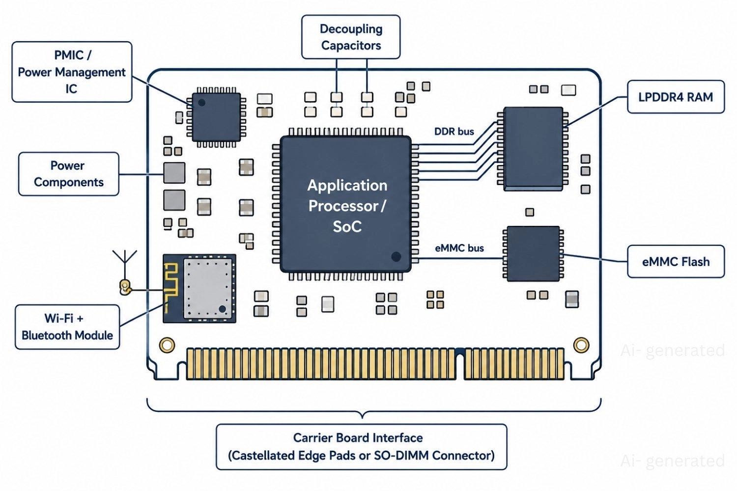
Figure: A system on module showing the application processor, LPDDR4 RAM connected via DDR bus, eMMC flash, PMIC, and Wi-Fi and Bluetooth module with antenna integrated on a single PCB.
System on Module vs Chip-Down Design: The Real Tradeoffs
This is the central question the title promises to answer. Both approaches are valid engineering choices. The right answer depends on volume, expertise, and timeline.
What Is Chip-Down Design?
Chip-down design means placing the bare SoC and every support component - RAM, flash, PMIC, RF front-end, crystal, decoupling network - directly on your product PCB. You own the DDR routing, the power sequencing, and the RF layout. The resulting board is fully custom, at the cost of significant engineering depth and development time.
When a System on Module Is the Better Choice
SoMs win on the dimensions that matter most for low-to-mid volume products and first-generation hardware:
- DDR memory routing - LPDDR4/LPDDR4X interfaces require extremely tight timing margins and carefully length-matched routing. A stackup change or layout revision can invalidate previously validated timing. On a SoM, this is the module vendor's problem, solved once and reused by every carrier.
- Power sequencing - Violating the processor's specified power-up sequence can cause startup failures or, in some cases, permanent device damage. SoMs integrate the PMIC and sequencing logic, reducing the carrier board's job to delivering a clean, stable input voltage.
- RF and wireless certification - Designing a 2.4 GHz or 5 GHz RF front-end requires antenna matching, SAR compliance testing, and FCC/CE lab testing that costs 10,000 USD to 40,000 USD and takes months. Pre-certified SoM wireless subsystems avoid this scope for the RF portion of the design.
- BSP and software support - SoM vendors provide validated Linux BSPs, real-time kernels, device trees, and update infrastructure. Building and maintaining an equivalent BSP for a chip-down design requires dedicated firmware engineering resources over the product's lifetime.
- Time-to-market - One study cited by Ezurio reported a 9 to 12 month reduction in IoT product development timelines using SoMs versus full custom designs. Even without that specific figure, the absence of DDR bring-up and RF validation alone can eliminate one to three board spins.
Important: Pre-certification on the module's wireless subsystem does NOT eliminate all compliance work. The final assembled product still requires its own FCC/CE testing, as the carrier board, enclosure, and cable assembly all affect radiated emissions. Modular certification reduces scope and cost but does not replace end-product testing.
When Chip-Down Design Makes Sense
- High volume - At 50,000 to 100,000+ units per year, the lower per-unit BOM cost of bare chips versus a complete module begins to overcome the higher NRE. A bare SoC costs less than a module that bundles RAM, flash, PMIC, and RF circuitry.
- Extreme size or power optimization - When every cubic millimeter and milliwatt matters (hearing aids, implantables, sub-1 W sensor nodes), chip-down placement and integration achieve densities no standard module format permits.
- Special hardware requirements - Products needing radiation hardening, temperature ranges beyond commercial SoM specifications, or custom silicon integration have no viable SoM option.
Quick Selection Guide
| If Your Product Needs... | Choose |
|---|---|
| Fast launch | SoM |
| Wireless certification | SoM |
| <50k units/year | SoM |
| Lowest possible BOM | Chip-down |
| Ultra-compact form factor | Chip-down |
| Existing DDR expertise | Chip-down |
Understanding the Cost Crossover
The cost crossover is the volume at which chip-down design becomes cheaper per unit than an SoM, when the full cost picture is included: NRE, BOM, certification, maintenance, and engineering time.
- Oxit (IoT engineering services): breakeven "typically falls between 50K and 100K units." Their LoRa example: 4.42 USD/unit chip-down versus 7.30 USD/unit module at 100K annual units.
- Avnet Silica: chip-down is "most suitable for products sold in large quantities, typically more than 50,000 units annually."
- Critical Link / Arm developer materials: breakeven can be as low as "around 3,000 units per year" when NRE amortization, ongoing maintenance costs, and an 18-month ROI window are factored in.
The wide range (3,000 to 100,000 units) reflects real variation. A product with complex wireless certification, a large BSP, and a small team shifts the crossover toward higher volumes. A product with simple connectivity, an existing reference BSP, and an in-house DDR layout expert shifts it lower.
The crossover is not a fixed number. It depends on product complexity, certification scope, in-house expertise, NRE budget, and how you account for engineering time.
| Factor | SoM | Chip-Down |
|---|---|---|
| NRE cost | Low, as the vendor handles DDR, RF, and PMIC | High, requiring full board design, RF layout, and BSP |
| Per-unit BOM cost | Higher, because the module bundles components | Lower, since bare chips cost less |
| PCB complexity | 4-6 layers (carrier board) | 8-12+ layers (DDR + RF) |
| Time to first hardware | Weeks to months | 6-18 months typical |
| DDR layout expertise | Not required | Required |
| RF design expertise | Not required (pre-certified wireless) | Required |
| Wireless cert cost | Reduced, with modular cert on module | Full FCC/CE lab testing required |
| Volume break-even | Better below 50k–100k units/year | Better above 50k-100k units/year |
| BSP maintenance | Vendor provides ongoing updates | Internal or contractor responsibility |
SoM vs SoC vs SBC
To successfully design a custom embedded product, it is essential to distinguish between silicon components, integrated modules, and fully built prototyping boards. These categories are often confused but serve entirely different functions in a production lifecycle.
| Feature | SoC | SoM | SBC | Chip-Down |
|---|---|---|---|---|
| What it is | Single silicon chip | SoC + RAM/Flash/PMIC on a small board | Complete computer with I/O ports | Fully custom board from bare chips |
| Ready to use | No - it is a component | No - needs carrier board | Yes, out of the box | No - full development cycle required |
| Customization | None (it is a part) | High, with a custom carrier board | Low - fixed I/O layout | Total - every component your choice |
| Design risk | Very high | Low to medium | Lowest | Highest |
| PCB complexity | High, at 8–12+ layers | Medium, with carrier 4–6 layers | N/A | High, at 8–12+ layers |
| Best volume | Very high | Low to mid | Prototyping/ hobby | High (50k+ units/year) |
| Cert overhead | Full FCC/CE required | Reduced if wireless pre-certified | N/A for product embedding | Full FCC/CE required |
| Example | NXP i.MX 8M Plus | Toradex Verdin, Raspberry Pi CM5 | Raspberry Pi 5 | Custom IoT gateway mainboard |
Is the Raspberry Pi a System-on-Module?
The standard Raspberry Pi 5 is a single-board computer (SBC) — it has USB, HDMI, Ethernet, and GPIO headers and runs out of the box. It is not a SoM.
Conversely, the Raspberry Pi Compute Module 4 and CM5 are genuine SoMs. They strip away standard connectors and expose the BCM processor and memory through high-density board-to-board connectors, requiring a custom carrier board to operate.
What Is the Difference Between a SoM and an SBC?
An SBC is a finished, standalone computer with fixed I/O layouts. A SoM has no standard connectors and does nothing by itself; it plugs into a carrier board designed by your team, giving you full control over product physical dimensions and external I/O.
SoM Architecture and the Role of the Carrier Board
What Is a Carrier Board?
A carrier board is a custom PCB that hosts a system on module. It provides power input, peripheral connectors (USB, Ethernet, HDMI, camera, GPIO), and application-specific circuitry. The SoM handles the complex, high-speed compute subsystem; the carrier handles the product-specific I/O.
What Stays on the SoM?
Everything that requires high-speed impedance-controlled routing or specialized RF design lives on the module:
- CPU/SoC and its internal power domain
- DDR memory (LPDDR4/LPDDR4X) with fully timed, length-matched traces
- eMMC flash
- PMIC and startup sequencing logic
- Wi-Fi/BT module with matched antenna (on wireless variants)
- Crystal oscillators and PLLs
- Blind and buried vias enabling dense routing within the compact module footprint
This work is validated once across temperature, voltage, and EMC by the module vendor. Every carrier board inherits that validation without re-spinning it.
What Goes on the Carrier Board?
The carrier board handles application-specific I/O and power entry:
- Input power connector with protection (reverse polarity, overvoltage, inrush limiting)
- DC/DC regulation providing the SoM's input voltage rail
- USB host/device connectors
- HDMI, DSI, or LVDS display output
- Ethernet PHY and RJ45 (if not integrated in the module)
- Camera connector (MIPI CSI-2)
- Industrial interfaces - CAN bus, RS-485, RS-232
- Sensor connectors and ADC inputs
- Real-time clock with battery backup
- Any I/O unique to the product
Because high-speed complexity lives on the module, carrier boards typically need only 4–6 layers and are manufacturable at standard PCB fabrication shops. A chip-down design with DDR memory typically requires 8–12 layers, HDI stackups, and tighter impedance tolerances throughout.
Common SoM Connector Types
The mechanical interface between SoM and carrier affects ruggedness, upgradeability, and cost:
- Board-to-board (mezzanine) - e.g. Hirose DF40. Raspberry Pi CM4 and CM5 each use two 100-pin high-density connectors. Socketed, swappable, field-upgradeable.
- SO-DIMM edge connector - same form factor as laptop RAM. Toradex Verdin uses a DDR4 SO-DIMM edge connector; NVIDIA Jetson Orin Nano uses a 260-pin SO-DIMM. Rugged, cost-effective, allows module swap without soldering.
- Castellated edge / solder-down - castellated half-vias soldered directly to carrier pads. ESP32-WROOM modules use this approach. Lowest profile, most vibration-resistant, not field-swappable.
- LGA solder-down - land grid array pads on the module underside, reflowed directly. Used by OSM-standard modules. Extremely compact; permanent attachment.
Tradeoff: socketed connectors allow swap and upgrade at the cost of added height and connector price. Soldered connections are the most rugged and compact, but permanent.
Carrier Board Design Workflow
A typical SoM-based product development cycle follows a structured sequence that shifts focus from processor design to system-level integration:
- Define processor and interface requirements.
- Select a compatible SoM family.
- Plan connector placement and mechanics.
- Design the carrier board power tree.
- Route high-speed interfaces.
- Validate signal and power integrity.
- Prototype and verify.
- Prepare for compliance testing and production.
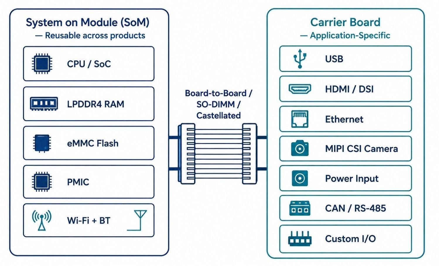
Figure: Architecture diagram showing a system on module, connected through a board-to-board, SO-DIMM, or castellated connector to an application-specific carrier board.
System on Module Benefits
Faster Time-to-Market
SoMs remove the most iterative and failure-prone design steps. The 9 to 12-month development timeline reduction cited by Ezurio for IoT products comes from eliminating DDR layout spins, memory subsystem validation, and BSP porting — all of which are parallel-path blockers that delay first hardware.
Reduced Hardware Risk
LPDDR4 and LPDDR4X routing requires extremely tight timing margins and carefully length-matched routing. A stackup change or layout revision can invalidate timing on a chip-down board. RF front-end design adds antenna matching, keep-out management, and SAR compliance. On a SoM, both are validated by the vendor before the module ships.
Carrier boards handle lower-speed signals - USB 2.0 at 90 ohm differential, HDMI at 100 ohm, I2C at a few MHz - where first-pass success rates are substantially higher. For controlled impedance best practices on your carrier, see JLCPCB's layout guidelines to prevent reflection and signal attenuation on transmission lines.
Easier Certification
Pre-certified wireless modules carry FCC and CE modular approval for the RF subsystem. Using one means the antenna, RF front-end, and radio stack were tested in an accredited lab before you receive the module.
Important: This does not eliminate end-product compliance. Your carrier board, enclosure, and cable assembly affect radiated emissions. The finished product still requires its own FCC/CE testing. Modular certification reduces scope and cost; it does not replace the final test.
Long-Term Availability
Industrial SoMs ship with 10 to 15-year availability commitments. Compulab guarantees 15 years of production. Toradex's Verdin family is committed through at least 2036. When a processor reaches EOL, pin-compatible module upgrades within the same family let teams update compute without redesigning the carrier board.
Scalable Product Families
One SoM can power multiple products. A low-cost carrier and a high-performance carrier can both use the same Raspberry Pi CM5 or Toradex Verdin module. A carrier board update does not require re-validating the compute subsystem - the module validation carries over.
| Benefit | What It Avoids | Practical Impact |
|---|---|---|
| Faster time-to-market | DDR routing, memory bring-up, BSP porting | Up to 9–12 months saved (Ezurio-cited) |
| Reduced hardware risk | Failed DDR spins, RF re-layout cycles | Higher first-pass PCB success rate |
| Easier certification | Full RF lab testing scope | Reduced FCC/CE cost and timeline |
| Long-term availability | SoC EOL product disruptions | 10–15-year module production common |
| Scalable product families | Full redesign per product variant | One carrier per product, shared module |
| Simpler carrier PCB | 8–12-layer HDI requirements | 4–6-layer carrier, standard fabrication |
System on Module Examples and Applications
Common System on Module Applications
While some compute subsystems are built using custom chip-down techniques, specialized System on Module solutions are standard in several demanding hardware sectors:
- Industrial Automation: Human-Machine Interfaces (HMIs), rugged programmable logic controllers (PLCs), and industrial gateways utilize the long lifecycle guarantees and extreme operating temperature ranges of industrial ARM modules.
- Medical Devices: Diagnostic imaging systems, clinical ventilators, and portable physiological monitors leverage pre-validated SoM hardware to simplify strict medical compliance pathways.
- Robotics: Automated Guided Vehicles (AGVs) and collaborative robotic arms employ modules with highly integrated GPUs or NPUs to handle complex localization and real-time path planning.
- IoT Gateways: Fleet management trackers and power-grid monitors combine integrated low-power microcontrollers with pre-certified cellular and Wi-Fi modules.
- Edge AI: Smart retail cameras and predictive maintenance arrays utilize high-performance neural processing modules to run image classification and detection models directly on-site.
- Transportation Systems: Infotainment systems and digital dashboards in commercial trucking utilize socketed or soldered SoMs because of their high resistance to continuous vibration and thermal cycling.
ESP32 Modules: A Lightweight Introduction to Modular Embedded Design
The ESP32-WROOM-32 is the industry standard for entry-level modular design. It is a highly integrated wireless microcontroller module containing the ESP32 SoC, flash, high-frequency crystal, and matched RF front-end on an 18 x 20 mm footprint.
Designers select this form factor to bypass the layout challenges of high-frequency RF trace routing and antenna matching. For developers interested in custom RF implementation and advanced wireless integration, studying the official guide on how to design an ESP32-S2 module PCB can provide great architectural and trace routing insights.
Raspberry Pi Compute Module 5
The Compute Module 5 (CM5) extracts the full computational throughput of the Raspberry Pi 5 single-board computer into an unshielded 55 x 40 mm form factor. Designers choose the CM5 to rapidly scale existing software prototypes into commercial, space-constrained products while inheriting Raspberry Pi's massive open-source library ecosystem and guaranteed long-term availability commitments.
Industrial ARM SoMs - Toradex Verdin
The Toradex Verdin is built for extreme reliability in harsh operating environments, such as factory floor automation, critical medical systems, and transport logistics. Featuring NXP i.MX 8M Plus processors and pin-compatible footprints across different performance classes, it allows engineering teams to swap modules without modifying the carrier board layout. This makes it the preferred architecture for hardware intended to run continuously for over a decade.
NVIDIA Jetson for Edge AI
The NVIDIA Jetson Orin Nano targets edge AI, robotics, and computer vision. By integrating a multi-core ARM processor with an Ampere-architecture GPU, it delivers up to 67 TOPS of machine learning execution directly at the edge. Hardware engineers choose this module to bypass the layout complexity of routing multi-channel LPDDR5 memory arrays and multi-rail power delivery networks.
| Module | Core SoC | RAM | Connector | Best For |
|---|---|---|---|---|
| ESP32-WROOM-32 | Dual Xtensa LX6 @ 240 MHz | 520 KB SRAM + 4 MB flash | Castellated 38-pin solder-down | Wi-Fi/BT IoT, hobby to product |
| ESP32-S3-WROOM-1 | Dual Xtensa LX7 @ 240 MHz | 512 KB SRAM + 8 MB flash | Castellated solder-down | BLE 5.0, AI instructions, Wi-Fi |
| Raspberry Pi CM5 | BCM2712 (4x Cortex-A76 @ 2.4 GHz) | 2/4/8/16 GB LPDDR4X | Two 100-pin board-to-board | Mid-range Linux products |
| Toradex Verdin iMX8M Plus | NXP i.MX 8M Plus (4x Cortex-A53) | LPDDR4, 2.3 TOPS NPU | DDR4 SO-DIMM edge | Industrial, vision, Industry 4.0 |
| NVIDIA Jetson Orin Nano | 6x Cortex-A78AE + Ampere GPU | 4/8 GB LPDDR5 | 260-pin SO-DIMM | Edge AI, robotics, vision |
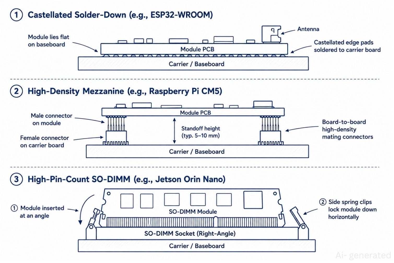
Figure: Comparing the physical mounting profiles, clearances, and connection interfaces of castellated, mezzanine, and SO-DIMM card-edge system on modules.
Designing a Reliable SoM Carrier Board
Carrier Board Planning Checklist
Before opening your schematic capture tool, use this planning checklist to map out your carrier board's critical constraints. Answering these questions early avoids costly architectural changes mid-design.
| Design Step | Key Questions |
|---|---|
| Processor | Does the chosen SoM family offer adequate compute margin and thermal headroom for your code? |
| Interfaces | Have you mapped out exactly how many high-speed USB, HDMI, PCIe, and CAN lanes must be routed? |
| Power | What is the input source voltage (e.g., 12V DC), and can your power tree supply peak current under load? |
| Thermal | Will the module require a passive heat spreader, an active heatsink, or direct chassis coupling? |
| Connectors | Should you use a socketed SO-DIMM or mezzanine board-to-board connector for field upgrades? |
| Manufacturing | Is your layout compatible with standard multilayer stackups, and have you checked SMT Sourcing options? |
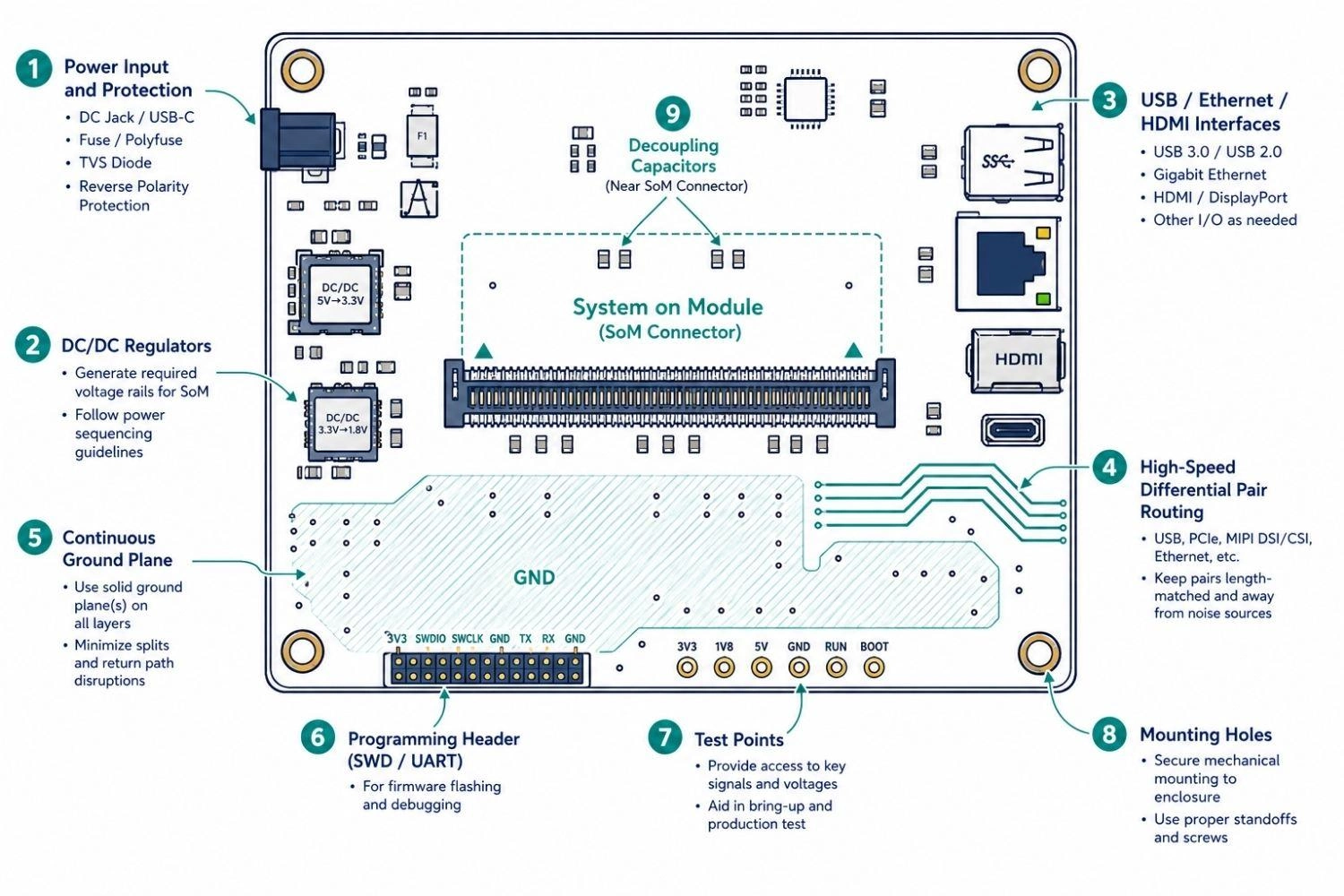
Figure: A System on Module carrier board highlighting the placement of the SoM connector, power circuitry, high-speed interfaces.
Power Architecture
The carrier board powers the SoM. The power entry stage must be robust:
- Input protection: reverse polarity diode or ideal diode controller; TVS or varistor for transient suppression; inrush current limiting (NTC thermistor or active soft-start circuit)
- EMI filtering: common-mode choke plus differential capacitors before the regulator input
- Regulation: LDO or DC/DC converter providing the SoM input rail (typically 3.3 V or 5 V - confirm in the module datasheet); verify PSRR and output noise specs, as some SoMs are sensitive to input ripple
Most SoM carrier boards can be implemented on standard PCBs, making them well suited for rapid fabrication and SMT assembly services.
Power Sequencing Considerations
Critical Warning: Violating the processor's specified power-up sequence can cause startup failures or, in some cases, permanent device damage. Always follow the module datasheet's power-on sequencing diagram - do not improvise.
Specific rules for carrier board power trees:
- Use the module's POWER_GOOD output and RESET_IN# signal to gate carrier-side peripherals
- Apply power to USB hubs, display controllers, and other carrier peripherals only after the SoM asserts its ready signal
- Add bulk capacitance on the SoM supply rail to prevent droop during inrush; verify minimum hold-up time in the datasheet
Signal Integrity and High-Speed Interfaces
Carrier boards handle lower-speed signals than chip-down boards, but several still require controlled impedance:
- USB 2.0 differential pairs: 90 ohm differential (45 ohm single-ended), matched length, no stubs, minimize vias in the pair
- USB 3.0 SuperSpeed pairs: 90 ohm differential, AC coupling capacitors per USB-IF specification, minimize layer changes
- HDMI / DSI: 100 ohm differential; keep pairs tightly coupled, route away from switching regulators
- Gigabit Ethernet: 100 ohm differential; place magnetics close to RJ45 connector, not close to the SoM
- PCIe (if used): 85 ohm differential; minimize via stubs with backdrill or avoid layer transitions where possible
Maintain continuous reference planes under all high-speed routes. Never route high-speed signals across splits in power planes. Keep return current paths short.
PCB Layer Count Considerations
Layer count requirements are significantly lower than chip-down designs, which often require 8 to 12 layers. A carrier board typically follows these stackup guidelines:
- 4 layers: suitable for USB 2.0, I2C, SPI, UART, no PCIe. Stack: signal / ground / power / signal.
- 6 layers: recommended with PCIe, USB 3.0, HDMI, or multiple power domains. Better reference plane continuity and power distribution.
- 8+ layers: rarely needed on carrier boards - only for PCIe Gen3+, multiple 10 GbE, or very dense I/O.
| Design Complexity | Recommended Layers |
|---|---|
| USB, UART, SPI | 4 |
| HDMI, USB 3.0 | 6 |
| PCIe Gen3 | 6–8 |
| Multiple 10GbE | 8+ |
Table: Typical Carrier Board Layer Count
The transition to dense, multi-layer carrier boards relies heavily on surface mount technology. Understanding the core layout differences of surface mount vs through hole design can help you optimize your component placement, routing densities, and SMT stencil layouts for trouble-free assembly.
Using Reference Designs
Start from vendor reference designs, not a blank schematic:
- Raspberry Pi - open-source CM4 and CM5 IO Board KiCad design files (schematic, layout, BOM) on official Raspberry Pi GitHub
- Toradex - carrier board specification document and reference schematics for all Verdin family modules
- NVIDIA - Jetson Orin Nano carrier board design guide, reference schematics, OrCAD/Allegro reference layout
Starting from a reference design catches known pitfalls - power rail voltage tolerances, reset timing, MIPI termination - before the first board is fabricated. Once the design is validated, low-volume assembled prototypes allow hardware and firmware teams to begin bring-up immediately.
Carrier boards designed from validated reference designs follow standard multilayer PCB rules and are straightforward to fabricate and assemble. JLCPCB supports 4 to 16 layer fabrication with full PCB assembly.
Design for Manufacturing (DFM) and Test (DFT)
Optimizing your carrier board for automated assembly and functional testing ensures reliable production yields. Focus on these key guidelines during layout:
- Provide fiducials for SMT assembly alignment.
- Keep adequate clearance around connectors for pick-and-place nozzles.
- Add SWD/UART test pads on a single board side for bed-of-nails testing.
- Ensure programming access to flash and bootloaders after final assembly.
Using professional assembly services allows your hardware prototypes and low volume PCB assembly runs to be delivered fully assembled and ready for firmware bring-up.
For production-ready carrier boards, PCB fabrication, stencil generation, component sourcing, and SMT assembly can all follow the same validated design files, ensuring maximum yield and consistent build quality.
Certification Checklist
Before formal regulatory testing, execute a pre-production checkout to verify basic system stability:
| Before Production Check | Target Verification Metric |
|---|---|
| Power rails validated | Validate power rails under load. |
| USB tested | Perform eye-diagram measurements. |
| Ethernet tested | Verify link and throughput. |
| Thermal verified | Verify thermal performance. |
| EMC pre-scan | Perform EMC pre-scan. |
| RF antenna clearance | Verify antenna clearance. |
| Programming header | Ensure programming access. |
Table: Pre-production check matrix listing targeted validation metrics for electrical, thermal, and regulatory checkout.
Choosing the Right System on Module
Committing to a SoM family shapes the carrier board pinout, BSP, and product upgrade path for the product's entire lifecycle. Evaluate these criteria before routing the first trace.
Processor Performance
Match the processor class to the application workload:
- Microcontroller-class (Cortex-M): real-time control, sensor acquisition, simple BLE/Wi-Fi IoT (e.g., ESP32, STM32-based SoMs)
- Application processor (Cortex-A): Linux applications, UI, camera, networking (e.g., Raspberry Pi CM5, Toradex Verdin, Variscite VAR-SOM)
- AI-accelerated (Cortex-A + NPU/GPU): computer vision, deep learning inference, robotics (e.g., NVIDIA Jetson Orin, Toradex Verdin iMX8M Plus)
Do not overprovision. An ESP32 module handles most sensor-to-cloud IoT tasks at a fraction of the cost and power of a Linux-class SoM. Reaching for a Jetson for a simple MQTT relay wastes power, BOM cost, and thermal headroom.
Connectivity Requirements
Verify interface availability in the module before routing the carrier:
- Cellular (LTE/5G): most SoMs do not include a modem, so plan for an external modem via USB or PCIe
- Wi-Fi 6 / Bluetooth 5.x: confirm which SKU variant includes wireless; many SoMs offer wireless and non-wireless versions
- Gigabit Ethernet: some SoMs integrate a GbE PHY; others expose RGMII requiring an external PHY on the carrier
- USB 3.0 / PCIe: check lane counts carefully; some modules offer shared-use lanes that cannot operate simultaneously
Interface assumptions discovered after carrier layout mean a costly respin.
Lifecycle and Support
For commercial products, lifecycle matters more than peak specification:
- Confirm stated minimum production lifetime (10+ years preferred for industrial products)
- Check for a pin-compatible upgrade path within the same connector family
- Verify OS support (Linux mainline or vendor BSP) is actively receiving security patches
- Check whether the vendor offers hardware repair or replacement programs
Ecosystem and BSP Quality
A SoM with a poor BSP is often worse than chip-down. Evaluate the following:
- Is the BSP based on a recent mainline Linux LTS kernel?
- Are drivers for all peripherals (camera, display, CAN, USB) included and actively maintained?
- Is there active community or vendor support, such as a forum, ticket system, or documentation depth?
- Does the vendor provide an OTA update framework, or must you build your own?
| Criteria | Questions to Answer Before Committing |
|---|---|
| Processor class | Cortex-M (RTOS) vs Cortex-A (Linux) vs NPU-enabled (AI)? |
| Required interfaces | USB 3.0 / PCIe / GbE PHY / MIPI CSI / CAN - does the module expose them natively? |
| Memory | RAM and flash adequate for OS + application + OTA update buffer? |
| Wireless | Wi-Fi/BT variant needed? Is a modular FCC/CE cert included on that SKU? |
| Lifecycle | Stated production lifetime? Pin-compatible upgrade path in the same family? |
| BSP quality | Mainline Linux kernel base? Active maintenance? OTA update support? |
| Connector type | SO-DIMM / board-to-board / castellated — matches form factor and ruggedness requirements? |
| Vendor support | Documentation depth, forum activity, hardware repair programs? |
| Target volume | Below or above the 50k–100k chip-down crossover threshold? |
| Certifications | Pre-certified wireless if needed? Track record of regulatory compliance? |
FAQs about System on Module
Q: What is a system on module?
A system on module (SoM) is a compact, ready-to-integrate circuit board that packages the core compute subsystem - processor, RAM, storage, and PMIC - onto a single module. It is not a standalone computer and must be mounted onto an application-specific carrier board to function.
Q: What is a carrier board?
A carrier board is a custom baseboard designed to host a system on module. It accepts input power, houses external I/O connectors (USB, HDMI, Ethernet), and provides any peripheral circuitry required for the final product.
Q: Is Raspberry Pi a system on module?
Standard Raspberry Pi models (like Pi 5) are standalone single-board computers (SBCs). However, the Raspberry Pi Compute Module series (CM4 and CM5) is a genuine SoM designed to be embedded onto custom carrier boards.
Q: Are SoMs more expensive than custom boards?
While a SoM has a higher per-unit BOM cost than bare silicon, it is significantly cheaper overall at low-to-mid volumes. The massive savings in upfront engineering hours (NRE), wireless compliance fees, and board spin-cycles easily offset the unit cost markup.
Conclusion
A System on Module (SoM) eliminates complex, pre-solved compute challenges like high-speed memory routing and RF validation. While chip-down design suits high-volume production (over 50,000 to 100,000 units annually) to lower BOM costs, a SoM drastically reduces time-to-market and hardware risk for low-to-mid volumes. Since true product differentiation lives on your custom carrier board, using a SoM lets you focus your engineering resources on unique product features.
Ready to build your carrier board? JLCPCB supports 4 to 16-layer PCB fabrication with full SMT assembly. Upload your Gerbers and BOM to get an instant online quotation and start prototyping your carrier board today.
Popular Articles
• PCB Silkscreen: All You Need to Know
• The Comprehensive Guide to Circuit Symbols: Key to Understanding Electrical and Electronic Diagrams
• Design Guidelines for PCB Using FR4 Substrates
• Choosing the Best PCB Color-Enhancing Aesthetics and Functionality
• PCB Board Design: A Step-by-Step Guide for Beginners
Keep Learning
ESP32 Power Consumption Explained: Current Draw, Sleep Modes, and Battery Life
Key Takeaways Power consumption by mode: The ESP32 draws around 240 mA during Wi-Fi transmission, 0.8 mA in light sleep, and just 10 µA in deep sleep, based on Espressif's typical datasheet figures. Deep sleep current: The ESP32 can draw 10 µA in deep sleep, with only the RTC timer and memory remaining powered. Keeping the ULP coprocessor running increases current consumption to around 100–150 µA. Development board power consumption: A typical ESP32 development board can draw around 6.5 mA even in dee......
ESP32 Pinout Reference: Which GPIO Pins Are Safe to Use and Avoid?
Key Takeaways GPIO count: The ESP32 chip has 34 GPIOs, and the ESP32-WROOM-32E module exposes 26 of them. General-purpose pins: Fifteen module GPIOs carry no boot, flash, or input-only restrictions: GPIO4, GPIO13, GPIO14, GPIO16 to GPIO19, GPIO21 to GPIO23, GPIO25 to GPIO27, GPIO32, and GPIO33. Strapping pins: GPIO0, GPIO2, GPIO5, GPIO12, and GPIO15 are sampled at reset, so any circuit connected to them must maintain the level required by the boot mode. Input-only pins: GPIO34, GPIO35, GPIO36, and GPI......
PCB Silkscreen: All You Need to Know
Key Takeaways The PCB Silkscreen Guide demonstrates that a properly designed legend layer is essential to prevent assembly failures and ensure long-term hardware reliability. By mastering modern manufacturing methodologies like Direct Legend Printing (DLP) and aligning layouts with JLCPCB's strict DFM design rules—including the absolute 0.8 mm character height limit and the automated 0.15 mm silkscreen clipping protocol driven by solder mask precedence—engineers can seamlessly eliminate cold joints an......
A Beginner's Guide to Basic Electronic Components: Functions, Symbols & Uses
Every circuit, from a simple LED flashlight to a microcontroller board, is built from the same handful of common electronic components. This guide breaks down the ten basic electronic components you will encounter most often: What each component does How it works Key specifications Where engineers use it By the end, you will be able to recognize these electronic circuit components on a schematic, a PCB, or a parts bin, and know exactly why each one is there. These electronic components are the buildin......
How to Read and Create PCB Schematics
Key Takeaways Read Schematics: Understand symbols, net labels, and component values. Design in EasyEDA: Place components and create circuit connections. Run Design Checks: Use ERC and DRC to identify potential issues. Verify Components: Check pin assignments and PCB footprints. Prepare for Manufacturing: Validate PCB layouts and manufacturing files. Printed circuit board (PCB) design begins with a clear understanding of how the electronic circuit should function. A schematic diagram represents the cir......
Maximizing Circuit Reliability with PCB Test Points and Smart DFT
Key Takeaways Early Fault Catching: Test points drastically reduce diagnosis time and prevent costly field failures. Standard Pad Sizing: Use 1.0 mm flat copper pads with 2.54 mm spacing for optimal fixture contact. Protect High-Speed Signals: Keep branch traces short to prevent capacitive loading and resonance. Single-Sided Access: Place all test pads on the bottom layer to cut fixture costs. Right Test for Volume: Use flying probe for prototypes and bed-of-nails ICT for mass production. A PCB test p......