
Low-Volume PCB Assembly for Startups and Prototyping
11 min
- Introduction: Beyond the First Prototype
- The Strategic Role of Low-Volume PCB Assembly in the Development Lifecycle
- Unique Technical Challenges in Low-Volume PCB Assembly
- Key Criteria for Selecting a Low-Volume PCB Assembly Manufacturer
- JLCPCB: A Platform Engineered for Low-Volume and Quick-Turn PCBA
- Design Optimization for Cost-Effective Low-Volume PCB Assembly
- Conclusion
- FAQs about Low-Volume PCB Assembly
Introduction: Beyond the First Prototype
The rapid advancement of the electronics industry has enabled the journey from a digital design to a physical product to be sped up. For startups, R&D labs, and individual makers, the ability to physically prototype and iterate time-sensitive solutions is not just a nice option; it is a necessity.
Low-volume PCB assembly is a specialty manufacturing service catering to the manufacturing of low quantities of populated circuit boards, in most cases ranging from a few boards to a few thousand boards.
This is more than simply a "small production run," it is a vital step in the New Product Introduction (NPI) process and is more typically referred to as small volume PCB assembly.
The small-volume PCB assembly serves a critical junction between a single hand-built prototype and the high-cost risk of manufacturing on a larger scale. It allows for design iteration for validation, hardware confirmation, and initial entry into the market planning, all while minimizing capital investment and risk.
This guide serves to provide an educational look into small-batch PCB assembly and the various considerations offered to engineers, from the challenges of low-volume PCBA to the fundamental metrics of selecting a PCBA manufacturer, as well as design rules to meet design for manufacture.
The Strategic Role of Low-Volume PCB Assembly in the Development Lifecycle
Low-volume production is a critical part of agile hardware development; it is an essential form of validation before a large capital commitment.
- Iterative Design and Hardware Validation: Small batches are essential for the build-test-learn cycle. They allow engineering teams to test their firsthand physical hardware in a real-world operating environment, test firmware, and identify discrete, underlying issues (such as signal integrity problems or thermal management inefficiencies) that cannot be tested in a simulation. This is the point where the prototype PCB assembly evolves into a product candidate.
- Design for Manufacturability (DFM) Analysis: The initial small batch is a practical test of a PCBA's manufacturability. It may uncover stark DFM and DFA (Design for Assembly) issues.
For example, a method to evaluate the initial batch may discover incorrect pad geometries, insufficient clearance for automated handling or assembly/semi-automated handling, and inadequate thermal profiles, etc., that may not have become problematic while evaluating a single, hand-assembled prototype, but would be potential problems in terms of yield potential and costs at scale.
- Early Market Seeding: For startups, low-volume PCB assembly is the most capital-efficient method to produce units for beta testers, key customers, or an initial product launch. This provides invaluable user feedback and validates market demand before committing to expensive high-volume tooling and component inventories.
Unique Technical Challenges in Low-Volume PCB Assembly
Although the fundamental PCB assembly process is similar to mass production, low-volume PCB assembly involves unique economic and logistical challenges that limit large-scale production systems. Careful decisions are required to complete production runs on time and within budget.
- Amortization of Non-Recurring Engineering (NRE) Costs: One-time tooling costs make up a portion of the NRE costs, for example, a solder paste stencil and machine programming fee. In a production run of 50,000 PCBAs, a $15.72 stencil cost (standard double-side) becomes negligible over the run at approximately $0.0003 per board.
In a production run of 50 PCBAs, the same $15.72 stencil cost is an additional $0.31 on the cost of every circuit board, plus the $50 setup fee adds $1.00 per board. These combined NRE costs ($1.31 per board total) become a major driver of the total low-volume PCB assembly cost.
| Production Volume | Fixed NRE Cost (Standard PCBA) | NRE Cost Added Per Unit |
|---|---|---|
| 50 Units (Low-Volume) | $65.72 ($50 setup + $15.72 stencil) | $1.31 |
| 50,000 Units (High-Volume) | $65.72 ($50 setup + $15.72 stencil) | $0.0013 |
Note: For complex stencil requirements (e.g., Large Size, electro polishing, irregular aperture, extensive spot counts, panelization), the stencil fee may increase substantially, but the per-unit impact remains minimal at high volume and becomes significant only in low-volume runs.
Also Read: In what cases will there be an extra charge for the stencil?
- Component Sourcing and Supply Chain Volatility: Sourcing electronic components to be used for small quantities becomes a particularly large hurdle in a low-volume PCB assembly.
Once procurement and purchasing personnel have done their research and determined component costs, larger distribution companies' MOQs often dictate purchasing larger quantities of parts or paying a premium for cut-tape supply. Again, this impractical increment in geometry increases costs and delivery timing as well for low-volume PCB assembly.
- Process Optimization and Yield: High-volume lines are optimized over thousands of units to improve the reflow profile and enhance yields. In a very low-volume run, there is no time for extended pre-established optimization. The process must be exact and robust from the first article. Controls and checks from the manufacturer become critically important.
Key Criteria for Selecting a Low-Volume PCB Assembly Manufacturer
From an engineer's perspective, selecting a manufacturer for small-batch PCB assembly requires prioritizing technical capabilities and process integration over raw price alone.
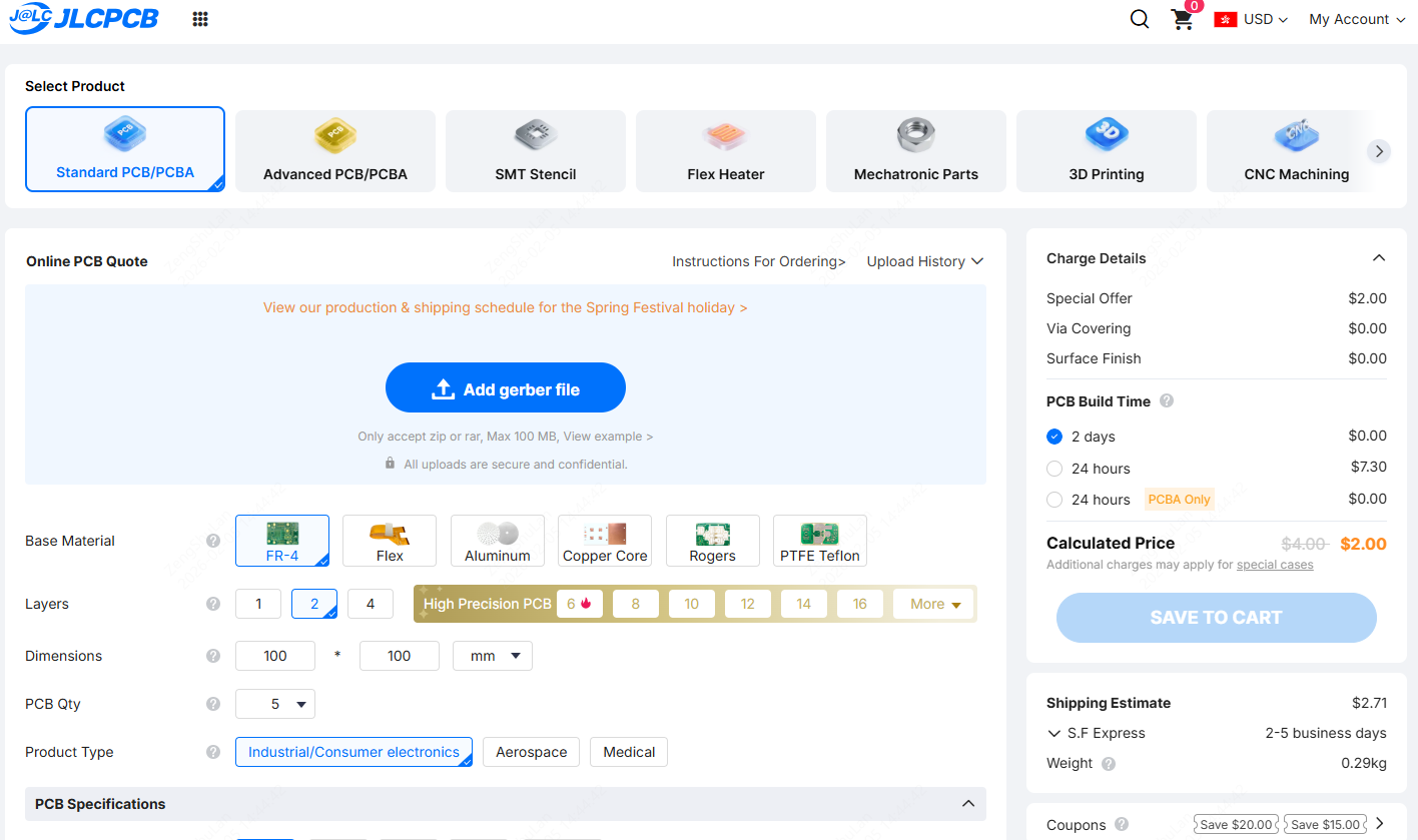
- Automated DFM/DFA Analysis: A top-tier low-volume PCB assembly manufacturer like JLCPCB provides instant, automated analysis of your Gerber, BOM, and Centroid files.
JLCPCB excels here by offering its powerful JLCDFM tool. This is more than a simple file check; it should flag potential manufacturability issues, such as silkscreen over pads, insufficient annular rings on vias, acid traps, and incorrect component spacing, that could halt an assembly line. This front-end feedback is invaluable.
Detailed DFM analysis of a designed PCB
- Integrated Component Sourcing Strategy: JLCPCB has a robust in-stock parts library. This solves the MOQ issue while also reducing risk for counterfeit components and simplifying the supply chain to be a single contact. What a value for smaller PCBA projects.
- Transparent & Instantaneous Quoting Engine: A contemporary online quoting engine should allow manufacturers and/or sourcing agents to break down pricing for raw components versus raw boards, stencil, and assembly labor quotes, all in one view online.
This would enable real-time analysis, as engineers themselves could swap out a component to update the BOM and instantly see the price implications for their design, becoming data-driven.
- Process Control & Quality Assurance: Make sure the PCBA manufacturer provides standard quality measures, like Automated Optical Inspection (AOI) for all batches, regardless of quantities.
For complex designs with BGA or QFN packages, confirm whether the manufacturer offers X-ray inspection. This is a non-negotiable quality gate in a process that ensures component placement and solder joint quality.
Comparison of a BGA component under visible light and X-ray inspection
JLCPCB: A Platform Engineered for Low-Volume and Quick-Turn PCBA
JLCPCB is specifically engineered to solve the core challenges of low-volume PCB assembly, making it an invaluable partner for startup projects.
- The Advantages of a Single Unified Ecosystem: Integrating PCB fabrication and assembly under a single vendor, like JLCPCB, offers a significant technical advantage. This unified approach simplifies logistics, as the entire process is managed through one interface. It streamlines the qualification of PCB assembly, as all components are delivered together, mitigating the risk of version mismatches that can arise when working with separate PCB manufacturers and assemblers.
- Addressing the Source Issue: JLCPCB’s extensive in-stock parts library is transformative. Electronics engineers can design with confidence, knowing they have easy access to a wide range of affordable components without the minimum-order-quantity hassles imposed by traditional distributors — all while enjoying much faster turnaround times.
- De-risking Production with Instant Quotes: Real-time quoting, online, provides immediate feedback on budgets. You can perform cost-optimization on the fly by substituting parts, adjusting board dimensions, and changing specifications before order commitment, which is a powerful approach to staying on a tight project budget.
- Seamless scaling from prototype to production: The same highly automated processes used for low-volume prototype runs (minimum order of 2 assembled PCBs and 3 bare PCBs) are applied to larger pilot runs, ensuring quality and reproducibility as your project scales. This approach eliminates the risk of configuration changes, allowing the exact board validated in the lab to reach your early customers.
JLCPCB PCBA Manufacturing Process
Design Optimization for Cost-Effective Low-Volume PCB Assembly
There are a few design techniques engineers can use to reduce costs and enhance manufacturability.
- Optimization of the Bill of Materials (BOM): The most effective way to reduce costs is to use components in the design that come from the JLCPCB’s in-stock library. By consolidating part numbers (e.g., using the same 0.1uF capacitor for every capacitor in the design), the design requires fewer individual reels to be placed in the pick-and-place machine and reduces assembly costs.
- Strategy for Layout and Panelization: For automated assembly—regardless of production volume—the industry standard is to include fiducial marks on the PCB.
For small-run boards, panelization is highly recommended. This involves placing multiple copies of a PCB onto a single, larger panel so they can be processed as one unit. Proper panelization significantly improves assembly-line performance and efficiency and often reduces the per-board assembly cost.
A panelized PCB with multiple boards arranged in an array to optimize the efficiency of the low-volume assembly process.
Conclusion
In the current competitive environment, it is a serious mistake to treat low-volume PCB assembly as just a stopover to mass production. It is its own distinct and powerful stage in the New Product Introduction development lifecycle, and it is where agile innovation takes place. This is where the design is really shaped, validated, improved, and de-risked before making significant investments in scale. To succeed requires more than merely sourcing a supplier; it requires strategy.
The main challenge is dealing with the economics of small batches, including high NRE costs and complicated component sourcing. This is why selecting the right manufacturing partner is a key engineered decision. An optimized platform like what JLCPCB offers can turn a historically complicated process into an elegant and easy-to-use tool by integrating fabrication, part sourcing, and assembly.
That said, when engineers tap into these specialized services and use judicious design optimization techniques, they can increase their speed to market. The value is in enabling engineers to optimize financial risk and launch validated and reliable products faster than ever. Selecting the right low-volume PCB assembly manufacturer is not just about manufacturing; it is about enabling innovation.
FAQs about Low-Volume PCB Assembly
Q: How much does low-volume PCB assembly cost?
A: The cost is a sum of the bare PCBs, a one-time stencil fee (NRE), the total cost of components, and assembly labor. While per-unit costs are higher than mass production, platforms like JLCPCB minimize NRE and sourcing costs, making small batches highly affordable.
Q: What is the lead time for small-batch PCB assembly?
A: With a quick-turn PCB assembly specialist, lead times are remarkably short. Assembly can often be completed in 24-48 hours, with a total order-to-delivery time of around 3-7 business days.
Q: Can you do prototype and low-volume PCB assembly together?
A: Yes. Leading manufacturers use the same automated production lines for both prototypes and small batches. This ensures a seamless transition, as the quality and manufacturing processes are identical, allowing for a smooth ramp-up from a few prototype units to a larger batch.
Q: SMT vs. through-hole for small batches: What are the trade-offs?
A: For automated assembly, SMT is almost always more cost-effective, even for small batches, due to the high speed of pick-and-place machines. Through-hole often requires manual insertion or slower selective soldering, which increases labor costs. However, through-hole provides superior mechanical strength for components like large connectors.
Q: What are the main challenges of low-volume PCB assembly?
A: The primary technical challenges are the high per-unit impact of NRE (setup) costs, sourcing components with high MOQs from distributors, and ensuring process accuracy from the very first board without the benefit of a long optimization run.
Q: How can I optimize my BOM for low-volume PCB assembly?
A: The best practice is to prioritize components listed in your assembler's in-stock library. This avoids sourcing delays and leverages their bulk purchasing power. Ensure all part numbers are active and have sufficient stock before ordering.
Popular Articles
Keep Learning
Turnkey PCB Assembly Explained: Full vs Partial Process And Benefits
Turnkey PCB Assembly offers a streamlined way to bring electronic products from design to production by handling component sourcing, PCB fabrication, assembly, and quality control under one service provider. For teams facing long lead times, complex BOM management, or repeated communication across multiple vendors, a turnkey solution eliminates these bottlenecks and significantly reduces the risk of production delays. By consolidating procurement and assembly into a single workflow, turnkey PCB assemb......
Low-Volume PCB Assembly for Startups and Prototyping
Introduction: Beyond the First Prototype The rapid advancement of the electronics industry has enabled the journey from a digital design to a physical product to be sped up. For startups, R&D labs, and individual makers, the ability to physically prototype and iterate time-sensitive solutions is not just a nice option; it is a necessity. Low-volume PCB assembly is a specialty manufacturing service catering to the manufacturing of low quantities of populated circuit boards, in most cases ranging from a......
PCB Assembly Manufacturing Process - JLCPCB Factory Tour
Printed circuit board assembly (PCB assembly manufacturing) is where a circuit design becomes a functional electronic product. Even with a perfectly fabricated PCB, poor assembly processes can lead to defects, reliability issues, and costly rework. In this factory tour, we walk through the complete PCB assembly manufacturing process at JLCPCB—from solder paste printing and automated component placement to reflow soldering, inspection, and final quality control. You'll see how a modern PCB assembly lin......
Low-Cost and Rapid Prototype PCB Assembly Service
For hardware developers, electrical engineers, and entrepreneurs, the most critical stage of product development is the transition from digital design to a physical prototype. Bringing a great schematic to life as a fully functional board is the ultimate goal—though historically, this has been the most costly and time-consuming phase of the process. This is where prototype PCB assembly becomes the key manufacturing stage, where electronic designs are physically realized for the first time. This articl......
Printed Circuit Board Assembly (PCBA): A Step-by-Step Guide
Printed Circuit Board Assembly (PCBA) is the process of mounting electronic components onto a fabricated PCB through solder paste deposition, SMT placement, reflow soldering, inspection, and final testing. A well-controlled PCB assembly workflow is essential for electrical performance, reliability, and overall manufacturing yield. This guide provides a clear, step-by-step overview of the full Printed Circuit Board Assembly process. At JLCPCB, PCB manufacturing and assembly are integrated in one ecosys......
Selecting a PCB Assembly Manufacturer: Expert Engineer Tips
In the field of electronics, the final product's dependability rests on its Printed Circuit Board Assembly (PCBA). PCB assembly is the process of soldering electronic components onto the bare PCB itself. This complicated act of assembly is very important to the function of the product. Choosing a PCB assembly manufacturer should be viewed as a partnership decision. A competent manufacturer will serve as an extension of your engineering staff, providing important feedback on Design for Manufacturabilit......