
What Is a PQFP Package? Plastic Quad Flat Package Design, Footprint, and Assembly Guide
17 min
- What Is a PQFP Package (Plastic Quad Flat Package)?
- Why Is PQFP Package Still Used in Modern PCB Designs?
- Typical PQFP Package Sizes, Pin Counts, and Dimensions
- Internal Structure and Materials of PQFP Package
- When Should You Choose the PQFP Package?
- PQFP vs. QFN vs. BGA: Which Package Should You Choose?
- How to Design a Reliable PQFP Footprint (Land Pattern)
- Common PQFP Footprint Mistakes to Avoid
- Thermal Performance of PQFP Package
- Electrical Performance and Signal Integrity of PQFP Package
- Manufacturing and Assembly Considerations for PQFP Package
- Reliability Characteristics of PQFP Package
- Optimizing PQFP Designs for Production with JLCPCB
- FAQ about PQFP Package
- Conclusion: PQFP Package Design and Assembly
The Plastic Quad Flat Package (PQFP) is a widely used IC package in industrial, automotive, and embedded designs.
This article provides a practical, engineering-focused guide to PQFP package. It explains how PQFP is built, when it makes sense to use it, how it compares with newer package types, and what designers should consider in terms of footprint design, thermal performance, signal integrity, manufacturing, and reliability.
What Is a PQFP Package (Plastic Quad Flat Package)?
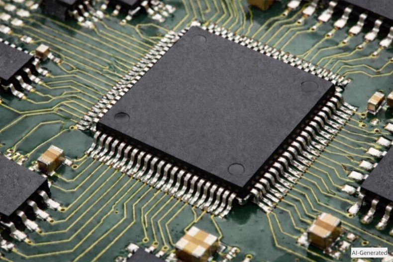
A Plastic Quad Flat Package (PQFP) is a surface-mount IC package with gull-wing leads extending from all four sides of a flat plastic body. Unlike leadless or area-array packages, every electrical connection remains exposed after soldering, making the joints easy to inspect, probe, and rework.
PQFP occupies a middle ground between low-pin-count packages and high-density formats. It supports significantly higher pin counts than SOIC or TSSOP packages without introducing the hidden solder joints and tight process control demanded by BGA devices. From a manufacturing standpoint, this reduces inspection risk and simplifies fault isolation during both production and field servicing.
Why Is PQFP Package Still Used in Modern PCB Designs?
Plastic Quad Flat Package (PQFP) is still used in real-world hardware designs where assembly reliability, inspection access, and long-term maintainability matter more than saving a few square millimeters of board space.
Although QFN and BGA packages are common in modern consumer products, they introduce hidden solder joints, tighter process control requirements, and limited rework options—factors that increase risk in many industrial and embedded designs.
In control systems, automotive electronics, and long-lifecycle embedded platforms, PQFP remains a practical choice because its gull-wing leads are easy to solder, visually inspect, and rework.
From a manufacturing perspective, it offers predictable yields and fewer assembly surprises compared to leadless or area-array packages. Electrically, it is sufficient for a wide range of clock speeds without forcing complex PCB stack-ups.
Typical PQFP Package Sizes, Pin Counts, and Dimensions
PQFP packages are standardized, but their physical size scales directly with pin count in a way that has real consequences for PCB layout and assembly. Unlike area-array packages, PQFP relies on perimeter leads, which means increasing I/O count inevitably increases package body size and board area consumption.
As pin count rises, the package grows deliberately to keep the lead pitch within a solderable and inspectable range. This controlled scaling is what makes PQFP forgiving to assemble, but it also explains why high-pin-count PQFPs occupy significantly more PCB area than QFN or BGA devices with the same number of connections.
For designers, this trade-off usually shows up as larger board outlines, longer trace lengths, or additional routing layers.
Common PQFP Package Characteristics
The table below reflects dimensions commonly encountered in production designs. Exact values vary by manufacturer, but these ranges are representative of standard JEDEC-compliant packages.
| Pin Count | Body Size (mm) | Lead Pitch (mm) | Max Height (mm) | JEDEC Standard |
|---|---|---|---|---|
| 44 | 10x10 | 0.80 | 2.35 | MO-112 |
| 100 | 14x20 | 0.65 | 2.80 | MO-112 |
| 160 | 28x28 | 0.65 | 3.40 | MO-112 |
| 208 | 28x28 | 0.50 | 4.10 | MO-208 |
| 240 | 32x32 | 0.50 | 3.40 | MS-022 |
Lower pin-count PQFPs are relatively compact and easy to route, making them suitable for simple control boards or moderate-density designs. Once pin counts exceed roughly 100, the package footprint grows quickly, and routing congestion becomes a primary concern.
At that point, the choice of lead pitch becomes critical: wider pitches such as 0.80 mm are far more tolerant of placement and solder volume variation, while 0.50 mm pitch packages demand tighter process control.
Practical Design Consideration
Note
One mistake that shows up again and again in PCB layouts is assuming that all PQFPs with the same pin count share an identical footprint. In reality, body size, lead length, lead width, and mechanical tolerances vary between manufacturers and even between devices from the same vendor. Relying on a generic footprint without verifying the datasheet often leads to assembly or reliability issues later.
Fine-pitch PQFPs (0.50 mm) deserve special attention. Insufficient solder mask clearance or excessive stencil aperture width can cause leads to sit slightly above the pads, creating open joints that may pass visual inspection but fail under thermal cycling. Ensuring adequate solder mask dams, accounting for lead coplanarity, and matching the stencil design to the specific package geometry is essential to avoid these hidden failures.
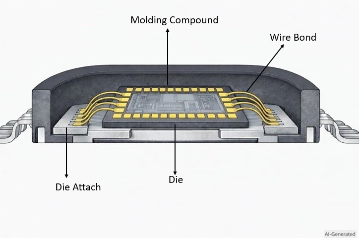
Internal Structure and Materials of PQFP Package
Internally, a PQFP uses a conventional lead-frame-based construction, which is one of the reasons it remains predictable in manufacturing and long-term use. At the core of the package is a copper alloy lead frame that provides both mechanical support and the electrical path from the silicon die to the PCB.
The silicon die is attached directly to the lead frame using conductive epoxy. This die-attach method offers a controlled thermal path from the die into the leads and, ultimately, into the PCB copper. While it cannot match the heat-spreading capability of exposed-pad or ceramic packages, it is adequate for the moderate power levels typically associated with PQFP devices.
Electrical connections between the die and the external leads are made using fine gold or copper wire bonds. Because these bonds are encapsulated within the molded body and not exposed to soldering heat, they are generally reliable as long as the package is operated within its specified thermal limits. From a design perspective, this places more emphasis on PCB-level heat dissipation rather than package-level cooling tricks.
After bonding, the assembly is encapsulated in an epoxy molding compound. This non-hermetic plastic enclosure protects the die and wire bonds from mechanical damage and environmental exposure, while keeping manufacturing costs low. The exposed gull-wing leads remain the only interface to the PCB, simplifying inspection and reducing uncertainty during assembly and rework.
The internal simplicity of PQFP is a practical advantage: fewer internal interfaces, well-understood materials, and predictable failure behavior. For PCB designers, this translates into fewer packaging-related surprises, especially in applications where reliability and serviceability matter more than aggressive thermal or size optimization.
The key internal elements found inside a typical PQFP package are summarized below:
| Component | Description |
|---|---|
| Package Body | Epoxy molding compound providing mechanical protection |
| Silicon Die | Active IC mounted on the lead frame |
| Die Attach | Conductive epoxy forming mechanical and thermal coupling |
| Wire Bonds | Gold or copper wires connecting die pads to leads |
| Lead Frame | Copper alloy structure providing electrical paths and support |
| Encapsulation | Non-hermetic plastic sealing |
When Should You Choose the PQFP Package?
PQFP is not a universal solution, but it fits well when practicality and predictability matter.
Choose PQFP Package if
- Pin count is moderate, and perimeter routing is acceptable
- Visual inspection and manual rework are required
- Cost control and flexible sourcing are important
- Long-term reliability matters more than size reduction
Avoid PQFP Package if
- The design involves very high-speed or RF interfaces
- Sustained high power dissipation is expected
- PCB area or package height is tightly constrained
Making this decision early avoids forcing PQFP into applications where another package is better suited.
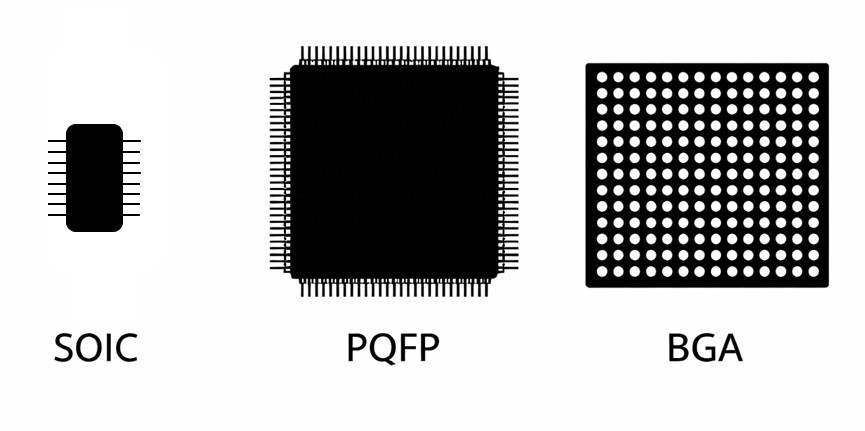
PQFP vs. QFN vs. BGA: Which Package Should You Choose?
Selecting the right IC package is a balancing act between performance, manufacturability, and cost. While Plastic Quad Flat Packages (PQFP) were once the industry standard, Quad Flat No-leads (QFN) and Ball Grid Arrays (BGA) have pushed the boundaries of miniaturization and thermal efficiency.
| Feature | PQFP (Gull-wing Leads) | QFN (Bottom Pads) | BGA (Solder Balls) |
|---|---|---|---|
| Footprint Density | Low (Large area) | Medium (Compact) | High (Extreme density) |
| Thermal Performance | Poor | Good (Thermal pad) | Excellent |
| Signal Integrity | Moderate (High inductance) | High (Short paths) | Superior (Best for High Speed) |
| Inspection | Easy (Visual) | Difficult (AOI/X-Ray) | Mandatory (X-Ray only) |
| Manual Rework | Easy | Moderate | Hard (BGA Station required) |
| Manufacturing Cost | Low | Low to Moderate | High |
Summary Recommendations
- Choose PQFP for prototyping, low-speed industrial controllers, or designs where manual rework is frequent and visual inspection is the only quality control available.
- Choose QFN for modern consumer electronics that need a balance of small size, good thermal performance, and moderate cost.
- Choose BGA for high-end processors (FPGA, GPU), high-density memory, and high-speed communication equipment where signal integrity and space are the top priorities.
How to Design a Reliable PQFP Footprint (Land Pattern)
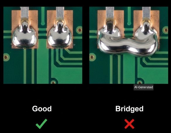
PQFP packages are mechanically forgiving, but they are not tolerant of careless footprint design. In practice, most PQFP soldering failures are not caused by the package itself—they originate from incorrect land patterns on the PCB. A poorly designed footprint can turn an otherwise reliable package into a consistent source of assembly defects.
Common problems such as solder bridging, weak mechanical joints, and intermittent opens usually trace back to pad geometry errors or insufficient spacing between leads. These issues often survive visual inspection and only surface during electrical testing or thermal cycling, when fixing them becomes expensive and disruptive.
General PQFP Footprint Guidelines
A well-designed PQFP footprint balances solder joint strength, inspection access, and manufacturing tolerance. The guidelines below reflect practices that have proven reliable in production environments rather than idealized textbook layouts.
| Design Element | Practical Guideline |
|---|---|
| Pad length | Provide sufficient toe and heel fillet without encouraging solder bridging |
| Pad width | Match lead width closely; avoid excessive pad overhang |
| Solder mask | Maintain clear mask dams between adjacent pads |
| Courtyard | Leave adequate clearance for inspection, probing, and rework |
Pad length is especially critical. Pads that are too short reduce the mechanical strength of the solder joint and make the connection sensitive to thermal cycling. Pads that are too long, on the other hand, increase the likelihood of solder bridging—particularly on fine-pitch devices. The goal is a visible toe fillet that confirms wetting without allowing solder to flow sideways.
Pad width should be derived directly from the lead dimensions specified in the device datasheet rather than copied from a generic library footprint. PQFP leads rely on controlled compliance during soldering, and excessive pad width reduces this compliance, increasing the risk of uneven joints when lead coplanarity is not perfect.
Design Takeaway
PQFP footprint design is not a cosmetic detail—it directly determines solder joint reliability. Treat the land pattern as a mechanical interface, not just an electrical connection, and verify it against the exact package geometry before committing a layout to production.
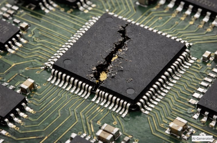
Common PQFP Footprint Mistakes to Avoid
One of the most frequent footprint mistakes with PQFP packages is reusing a land pattern across different lead pitches. A footprint that works acceptably for a 0.80 mm pitch device will almost always cause assembly problems when reused for 0.65 mm or 0.50 mm pitch parts. Even small changes in lead spacing and width can shift solder volume enough to create bridges, uneven joints, or intermittent opens.
Another common failure point is poor solder mask definition. Fine-pitch PQFPs rely heavily on solder mask dams to control solder flow during reflow. When mask openings are oversized or dams are missing, solder can spread laterally and bridge adjacent leads—especially on high-pin-count devices where spacing margins are already tight. These defects often look acceptable after reflow but show up later as electrical failures or marginal joints.
Before releasing a design for fabrication, a focused Design for Manufacturing (DFM) review is essential. DFM checks routinely catch problems that are easy to miss during layout, such as marginal pad spacing, inadequate solder mask clearance, or courtyard violations that complicate inspection and rework. Addressing these issues early avoids expensive fixes once boards are assembled.
In practice, a correct PQFP footprint does more than improve solder joints. It simplifies inspection, reduces rework risk, and keeps assembly results consistent as production scales. Most "PQFP problems" seen on the factory floor are footprint problems, not package limitations.
DFM Checks for PQFP Footprint Before Fabrication
Before sending a board out for fabrication, running a Design for Manufacturing (DFM) check is a smart step. These checks often uncover issues that are easy to overlook during layout, such as marginal pad spacing, solder mask definition problems, or clearance violations that can later show up as assembly defects.
In practice, a well-designed PQFP footprint does more than just improve solder joints. It makes inspection straightforward, reduces the risk during rework, and helps keep production consistent and predictable once the design moves to volume manufacturing.
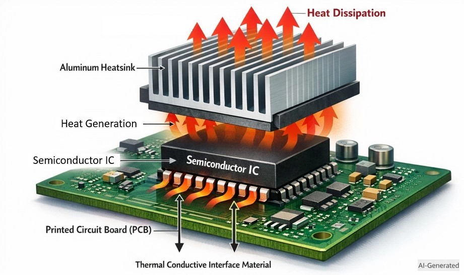
Thermal Performance of PQFP Package
PQFP packages are not intended to function as primary thermal solutions. Unlike exposed-pad or power-optimized packages, a PQFP relies almost entirely on the PCB to remove heat generated by the silicon. As a result, thermal performance is driven far more by board layout than by the package itself.
The plastic molding compound used in PQFP acts as a thermal insulator rather than a heat spreader. Heat leaves the device mainly through the leads and into the PCB copper connected to them. Because of this, junction-to-ambient thermal resistance (θJA) varies widely depending on copper area, layer count, and airflow around the board.
Typical Thermal Behavior of PQFP Package
| Aspect | Practical Impact |
|---|---|
| Mold compound | Poor thermal conductivity |
| Heat flow path | Primarily through leads into the PCB copper |
| θJA | Strongly dependent on board design |
| Power handling | Low to moderate, application-dependent |
In real designs, PQFP packages perform reliably when power dissipation is steady and kept within moderate limits. They are a poor choice for applications with sustained high heat or large thermal swings unless the PCB is specifically designed to compensate with increased copper area or thermal spreading.
When higher power density is unavoidable, selecting a package designed for heat removal is usually a safer decision than trying to push PQFP beyond its natural limits.
Improving PQFP Package Thermal Performance Through PCB Design
PQFP packages rely almost entirely on the PCB for heat removal. Heat leaves the device mainly through the leads and into the board, so copper distribution around the package is critical.
Connecting power and ground pins to larger copper areas helps spread heat, while thermal vias allow it to move into inner and bottom layers. Increasing copper thickness and providing modest airflow, when possible, further reduces junction temperature. With these measures, acceptable thermal performance can usually be achieved without changing the package.
Electrical Performance and Signal Integrity of PQFP Package
Electrically, PQFP is a stable and predictable package for low-to-moderate speed digital, mixed-signal, and control applications. The exposed gull-wing leads make probing and debugging straightforward, which is a practical advantage during development and servicing. While the leads add some inductance, this is rarely an issue in typical microcontroller or DSP designs and only becomes relevant at very high interface speeds.
Signal Integrity Best Practices for PQFP Package
Good signal integrity with PQFP depends mainly on PCB layout. Keep high-speed traces short, place decoupling capacitors close to power pins, maintain a continuous ground plane, and separate noisy digital signals from sensitive analog paths. Following these basics is usually sufficient for reliable operation.
Manufacturing and Assembly Considerations for PQFP Package
Moisture Sensitivity and Storage (MSL Considerations)
Like all plastic packages, PQFP can absorb moisture over time. If not controlled, this moisture can expand during reflow and cause internal damage.
Following the specified MSL handling rules, baking parts when required, and using dry storage for long-term holding are usually enough to prevent moisture-related failures. This becomes especially important in low-volume or prototype builds, where components may sit unused for extended periods.
Pick-and-Place and Reflow Guidelines for PQFP Package
PQFP packages work well with standard SMT assembly lines. The flat body and exposed leads make pick-and-place reliable, although fine-pitch variants require accurate placement to avoid lead misalignment. During reflow, controlled temperature ramp rates are important to limit mechanical stress and reduce moisture-related risks. Manufacturer-recommended reflow profiles should always be followed, especially for high pin-count or fine-pitch devices.
Inspection and Rework Advantages of PQFP Package
PQFP's exposed gull-wing leads make inspection and rework straightforward. Solder joints are easy to verify visually and with AOI, reducing uncertainty after assembly. Manual rework is also safer than with packages that hide their joints, since individual leads can be accessed without specialized tools. For this reason, PQFP remains a practical choice for prototypes, low-volume builds, and products that require field servicing.
Reliability Characteristics of PQFP Package
PQFP packages have a long and well-documented field history, which makes their reliability behavior predictable. When handled correctly, assembled with standard processes, and operated within specified limits, they deliver stable long-term performance.
The gull-wing leads provide mechanical compliance, allowing the package to tolerate vibration, thermal cycling, and minor PCB flex better than more rigid formats. Moisture resistance is adequate for most applications as long as standard storage and handling practices are followed. Like all plastic packages, PQFP is not hermetic, so reliability depends on controlled reflow and proper moisture management.
Thermal aging can become a concern in designs that operate continuously at elevated junction temperatures. However, when thermal limits are respected, PQFP devices have shown consistent performance across decades of industrial and embedded use. For many long-life products, this proven behavior outweighs the space savings of newer package types.
Optimizing PQFP Designs for Production with JLCPCB
Designing a perfect PQFP footprint is only half the battle; the real test happens during assembly. Even minor errors in pad alignment or solder mask clearance can lead to costly rework.
To ensure your design is production-ready, JLCPCB provides integrated solutions that bridge the gap between design and manufacturing:
- Free Online DFM Check: Before you place your order, use JLCPCB's DFM tools to detect potential solder bridging or clearance issues specifically for fine-pitch PQFP components.
- High-Precision SMT Assembly: With SPI solder paste inspection, advanced pick-and-place machinery, and automated optical inspection (AOI), JLCPCB ensures that every gull-wing lead is deposited, placed, and soldered with precise volume, alignment, and reliability.
- Reliable Components Sourcing: Avoid moisture-related "popcorning" with JLCPCB's strictly controlled component storage and baking processes, ensuring your PQFP chips maintain their MSL integrity.
FAQ about PQFP Package
Q: What is a PQFP package used for?
PQFP packages are commonly used in microcontrollers, DSPs, ASICs, and interface ICs, where moderate to high pin counts are required along with easy inspection and rework. They are widely found in industrial electronics, automotive ECUs, consumer appliances, and embedded systems.
Q: What is the difference between PQFP and LQFP?
The main difference lies in package height. PQFP is the standard-height plastic quad flat package, while LQFP (Low-Profile QFP) has a thinner body. Electrically, they are similar, but LQFP is preferred when vertical space is limited.
Q: Are PQFP packages moisture sensitive?
Yes. Because PQFP packages use plastic molding compound, they can absorb moisture over time. This is why moisture sensitivity level (MSL) handling, proper storage, and baking before reflow are important to prevent package cracking.
Q: What are the most common assembly problems with PQFP package?
Typical issues include solder bridging at fine pitch, coplanarity problems due to bent leads, and moisture-related damage during reflow. Most of these issues can be minimized with correct footprint design, proper handling, and a controlled reflow profile.
Conclusion: PQFP Package Design and Assembly
The Plastic Quad Flat Package (PQFP) remains relevant because it behaves predictably in real hardware. It may not be the smallest option available, but it offers stable electrical performance, straightforward assembly, and a reliability profile that engineers understand.
When footprint design, thermal limits, and basic manufacturing practices are respected, PQFP performs exactly as expected—making it a dependable choice for industrial, control, and embedded systems designed for long service life.
Popular Articles
• SMD Diode Code Lookup: Full List, Marking Guide & Identification [2026 Guide]
• SMD Resistor Package Sizes: Complete Size Chart, Footprints & How to Choose
• SMD Capacitor Codes: Identification, Markings, and Polarity
• SMD Capacitor Sizes: Complete Size Chart and Selection Tips for PCB Design and Assembly
• How to Solder SMD Components Like a Pro [2026 Updated]
Keep Learning
PoP Package (Package on Package) Explained: Architecture, Assembly, and SMT Challenges
In the race for miniaturization, fitting more processing power into smaller footprints is the ultimate challenge for PCB designers. Package on Package (PoP) technology answers this by integrating logic and memory vertically, becoming the standard for modern mobile processors. However, this 3D architecture demands advanced SMT assembly capabilities beyond standard fabrication. JLCPCB specializes in the high-precision manufacturing required to master these complex stacks. This guide covers how PoP packa......
What Is a PQFP Package? Plastic Quad Flat Package Design, Footprint, and Assembly Guide
The Plastic Quad Flat Package (PQFP) is a widely used IC package in industrial, automotive, and embedded designs. This article provides a practical, engineering-focused guide to PQFP package. It explains how PQFP is built, when it makes sense to use it, how it compares with newer package types, and what designers should consider in terms of footprint design, thermal performance, signal integrity, manufacturing, and reliability. What Is a PQFP Package (Plastic Quad Flat Package)? A Plastic Quad Flat Pa......
Small Outline Integrated Circuit (SOIC): Package, Specs & Uses
As designs transition from legacy through-hole components to high-density Surface Mount Technology (SMT), the Small Outline Integrated Circuit (SOIC) remains the industry standard for operational amplifiers, flash memory, sensors, and microcontrollers. It stands as a testament to balanced engineering, offering a perfect compromise between the miniaturisation demanded by modern consumer electronics and the ruggedness required for industrial applications. This article serves as a definitive engineering ......
A Complete Guide to Surface Mount Device (SMD)
Imagine holding a smartphone in your hand. Inside that sleek device lies a complex network of thousands of miniature components — resistors smaller than a grain of rice, capacitors thinner than a fingernail, and integrated circuits containing millions of transistors. Without Surface Mount Technology (SMT) and its compact Surface Mount Devices (SMDs), none of this would exist. Just a few decades ago, electronics were bulky. Radios filled desks, computers filled rooms, and assembling a circuit meant dri......
Circuit Breaker Types Explained: MCB, MCCB, RCCB, RCBO, ACB, VCB & SF6 Circuit Breakers
A circuit breaker automatically disconnects power when it detects faults such as overloads or short circuits, protecting equipment and reducing fire risk. Different circuit breaker types are designed for different voltage levels, current ratings, and applications, from household distribution boards to high-voltage substations. This guide explains the most common types - including MCBs, MCCBs, RCCBs, RCBOs, ACBs, VCBs, and SF6 breakers and helps you choose the right one for your application. Figure: Ci......
Quad Flat Package (QFP): The Engineer's Guide to Design, Assembly and Thermal Management
What is QFP Package? The Quad Flat Package (QFP) is one of the most popular surface mount technology (SMT) package formats throughout the history of electronic manufacturing. After it became standard in the 1980s, the QFP has been the industry standard for integrated circuits (ICs) with moderate to high pin counts that typically range from 32 to 304 pins, so it was a good alternative for simple SOIC packages and complex Ball Grid Arrays (BGAs) at the same time. Defined by its "gull-wing" leads extendi......