
PCB Etching in Professional Fabrication : Modern Techniques and Industrial Strength
12 min
- Chemical Etching Processes in Controlled Industrial Environments
- Evolution Toward Advanced Etching Techniques in Modern Fabrication
- Limitations of Traditional Etching and How Professionals Overcome Them
- Advantages of Professional PCB Fabrication Etching
- Frequently Asked Questions (FAQ)
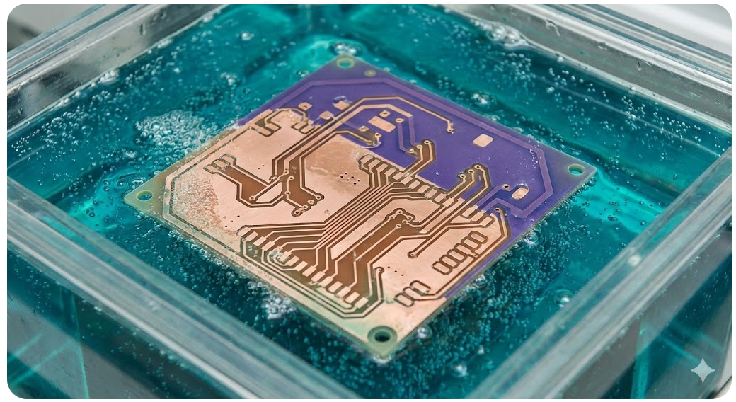
The etching of printed circuit boards is the selective removal of unwanted copper on a board to form the conductive traces and pads. It is effectively a subtractive process; after the photolithography or a printed resist mask has been applied, the remaining copper is removed with a chemical ether solution. It leaves the circuit pattern it was intended to create. Well, imagine that you are on the copper at the spa, you put it in the correct bath, and the undesired metal just dissolves. Etching is accurate and precise in designing complex circuit patterns. As we shall observe in this paper, despite the numerous emerging technologies, chemical etching continues to play a foundation in PCB manufacturing. Its key advantages are accuracy and uniformity. Etching can give very uniform and repeatable traces when carefully controlled.
In fact, experts note that the precision of etching directly impacts the board’s electrical performance and signal integrity. The process is self-limiting as it only eats away exposed copper and stops cleanly at the mask boundary. Unlike a mechanical cutter that might wander, a chemical bath dissolves copper evenly wherever it should. Modern photolithography aligns the resist pattern to within a few microns.
Chemical Etching Processes in Controlled Industrial Environments
Ferric Chloride and Ammonium Persulfate in Volume Production
In high-volume PCBs, the etching bath is designed to achieve throughput and cost-effectiveness. Ammonium persulfate and ferric chloride are two very common chemical etchants. Ferric chloride is a very corrosive liquid that reacts vigorously with copper. It reacts with copper, dissolving it and leaving the necessary circuit traces. It has the benefits of being inexpensive and readily available, but forms a deep-orange copper salt sludge, which needs to be safely disposed of. Ferric chloride is used in many factories to make boards with larger features or where the fineness of resolution is not very important.
An alternative such as ammonium persulfate, is used in high-volume production. Under controlled conditions, APS is not as toxic as ferric chloride and can be used to obtain higher etch rates. JLCPCB reports that APS is a non-toxic solution that offers a dependable etching solution. This is why APS is popular at many high-end fabs to use in fine-feature etching and inner-layer etching.
Automated Etching Lines and Precise Parameter Control
Professional PCB manufacturers do not etch boards by hand; they use highly automated etching lines. These systems are conveyorized and incorporate tight process controls. A typical sequence is: clean the board, apply a pre-wet rinse, spray etch from multiple nozzles, then rinse, neutralize, and dry. Throughout, the temperature is held constant often around 30–40 °C. The result is very uniform etching: no region is starved of chemistry, and boards come out consistently.
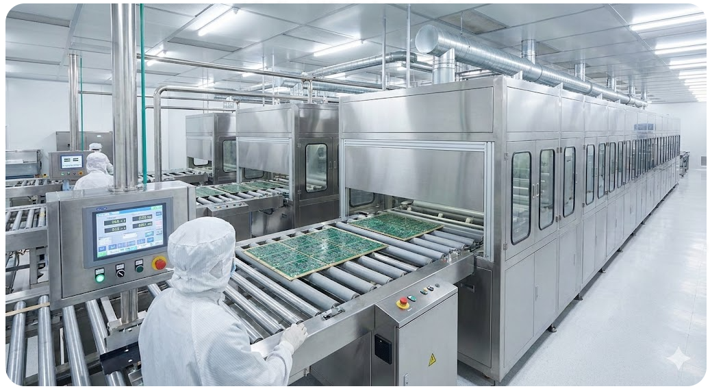
Modern factories are “shifting toward automation” with real-time monitoring and even AI-driven control. Inline sensors and gauges can detect the etch rate on the fly. For example, a thickness monitor might signal when enough copper has been removed, automatically stopping the process to prevent over-etch. An industry report notes: “Automated etching lines apply and remove photoresist, creating circuit traces with consistent width and spacing.”
Safety, Waste Management, and Environmental Compliance Standards
Safety and environmental control is also required during high-volume etching. Strong alkaline etchants such as ferric chloride or chemicals such as ferric chloride are also dangerous to human health and the environment. The etching stations in a professional plant are ventilated and sealed, the fumes are scrubbed, and spills are contained. Chemical protective gloves, aprons, and goggles are put on at all times by workers. More importantly, spent etching solutions and rinse water are never drained into the drain. Top PCB fabs employ closed-loop technology: copper is recycled off spent ferric chloride, and the remaining solution is neutralized to salts, which are not harmful.
These measures are needed since PCB production may produce a lot of toxic waste in case they are not controlled. As mentioned by one of the sustainability guides, the conventional etching emits toxic acids and heavy-metal effluent into the atmosphere. Top manufacturers to reduce this, adhere to stringent regulations such as RoHS and REACH.
Evolution Toward Advanced Etching Techniques in Modern Fabrication
Photolithography Integration for Higher Resolution
Today’s PCB fab lines tightly integrate photolithography and etching to achieve ultra-fine features. First, a photosensitive resist is applied to the copper-clad board. Next, a photomask or laser direct imaging tool exposes the circuit pattern onto the resist with high precision. The unexposed resist is washed away, leaving a detailed stencil of the desired copper. Only after this high-resolution pattern is in place does the board enter the etching bath. This method allows manufacturers to define traces and spaces down to tens of micrometers with excellent alignment between layers.
This integrated process supports complex multilayer and HDI boards. Each internal copper layer is patterned and etched separately, then layers are laminated together. Modern machines can align masks on different layers with sub-10μm accuracy. The combined photolithography-plus-etch approach enables circuitries far beyond what older printing or toner-transfer methods could achieve. In other words, the fine geometries in today’s professional PCBs are made possible by this photolithographic patterning followed by precise chemical etching.
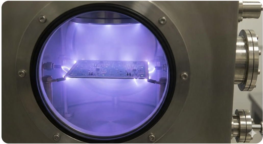
Plasma and Dry Etching for Fine-Line and Multi-Layer Boards
Advanced fabs use dry etching for certain critical tasks. In plasma etching, the board is placed in a vacuum chamber and bombarded with ionized gases. These energetic ions can remove copper or etch away dielectric material with nanometer precision. Plasma etching is especially useful for forming microvias. Because it can cleanly etch all the way through the copper and laminate.
Another major advantage of dry etching is reduced waste. Unlike wet etching, which produces spent chemical effluent, plasma leaves no liquid contaminants. As one technical guide observes, dry etching avoids the use of chemicals. The trade-off is cost and complexity the dry etch equipment is expensive, so it’s used selectively. Nonetheless, by combining even short plasma steps with traditional etching, modern fabs extend the capabilities of etching into domains that liquid baths alone cannot reach.
Hybrid Approaches Combining Chemical and Mechanical Methods
A multi-layer board might be chemically etched for its fine circuitry, but then routed or laser-cut for the outer shape and slots. Some processes are explicitly mixed in a semi-additive fabrication. A panel is first fully clad in copper, then a resist is patterned, and copper is electroplated onto the exposed areas, and finally, the original base copper is etched away. This combines additive (plating) and subtractive (etching) steps to create very thin, high-density traces with less waste. Even at the prototype stage, manufacturers offer multiple options. Many shops provide CNC milling for quick-turn boards alongside their chemical etch services. Others might use laser ablation to tweak a design.
A home enthusiast working with a simple ferric-chloride kit has only one method, but a professional fab can mill, laser, etch, and plate as needed. This flexibility allows complex designs to be fabricated economically and reliably. Modern PCB fabrication doesn’t view etching as an isolated step but as one tool in a larger toolbox.
Limitations of Traditional Etching and How Professionals Overcome Them
Challenges with Uniformity, Undercut, and Feature Size in Scaling
Physical limits to wet etching are present even in well-controlled wet etching. One of them is that the slight undermining of the etchant can creep under the edges of the resist, hence the traces end up having a trapezoidal shape. Minor undercutting might be acceptable, but serious undercutting can cause very thin traces to be weak or can change electrical impedance, particularly on high-speed lines.
The other concern is consistency on a boardwide basis. When the agitation or spray flow is not uniform, then certain areas may etch quickly than others, resulting in non-uniform etching and inconsistent trace widths. These non-uniformities may disturb signal paths or may make some boards on a panel fail inspection. Engineered processes are used to address these challenges by professional fabs. Their spray tanks are multi-stage, allowing the solution to be well-mixed, and they are very precise with time and temperature. Most etching lines have real-time thickness monitors, which can sense when a copper layer has been fully etched to prevent any over-etching.
Material Compatibility and Process Consistency Issues
Not all PCB materials etch the same way. Standard FR-4 is well-characterized, but specialty laminates may require adjustments. Some high-frequency boards use PTFE-based laminates that can delaminate if aggressive acid is used. Even the choice of photoresist or plating mask can affect etch outcomes. Because of these variables, a one-size-fits-all etch recipe won’t work for every material stack-up.
Industrial fabs handle this by profiling and adjustment. Before etching, each board’s copper thickness is measured, and the appropriate etchant formula is selected. Many factories maintain databases of etch rates for different copper weights and laminates. For instance, 2 oz copper boards stay longer in the bath than 0.5 oz boards. The parameters for each material type are stored in the machine recipes. This way, boards made of different materials etch with the same end result consistency.
Long-Term Trace Reliability in High-Density Designs
When traces become extremely small, any tiny etching imperfection can impact reliability. Very narrow copper lines have less margin for error and are more susceptible to mechanical and thermal stress. If an etch leaves microscopic notches or roughness on a thin trace, those can grow into cracks over many thermal cycles or vibrations.
To guard against this, professional boards typically get immediate protection after etching. In almost all industrial processes, the bare copper is quickly coated with a surface finish. Freshly etched copper gets a robust coating that prevents oxidation and strengthens the trace. Some boards may also undergo a polymer coating or solder mask, adding further protection. In high-reliability industries boards undergo rigorous validation. Sample boards might be thermal-shock tested, bent, or subjected to humidity to ensure the traces hold up. Any trace with a marginal etch profile could show a failure in such tests.
Advantages of Professional PCB Fabrication Etching
Superior Precision, Repeatability, and Yield Rates
The fabrication plants of PCB are designed to be precise. Controlled chemistries through automated etching give very tight tolerances. Frequently, a few micrometers of line width and high repeatability. This is translated into large yield rates; it is not unusual to have fabs with more than 95 percent first-pass yield on bare boards. Following the etching process, Factories are scanning all boards with Automated Optical Inspection (AOI). Missing copper, shorts, or mask defects are checked by high-resolution cameras. Any board that has an anomaly is flagged and checked. With early detection of errors, virtually all the manufacturing faults are removed prior to delivery.
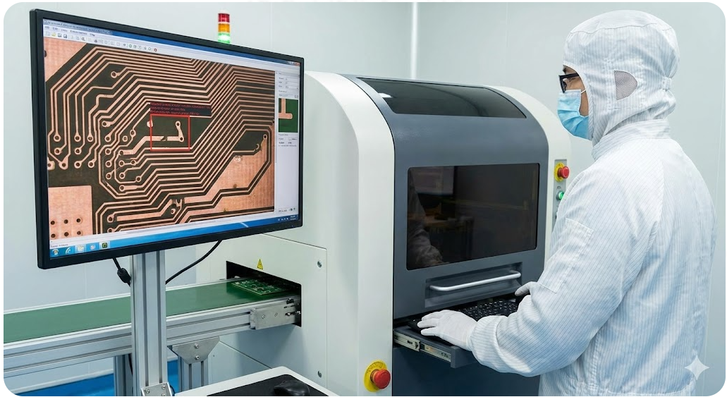
Practically, an industrially etched board will be uniform in trace widths, contain clean edges, and will not have unwanted residue. This uniformity is important with high-speed or high-density circuits. According to one industry source, automated etching is the only means of ensuring uniform trace widths when dealing with high-volume orders.
Integrated Quality Controls and Traceability Throughout Production
Great quality assurance and traceability are key benefits of professional fabrication. All batches of boards are tracked from raw material to the finished product. Each panel has a laminate batch number, type of copper foil, and etchant batch. Should a problem be discovered later, engineers can be able to track it down to the specific production run and even the lot of chemicals. Such traceability cannot exist in a DIY environment.
In addition to traceability, there are numerous inspections conducted during the process. Etched boards are frequently tested using electrical flying-probe test equipment to ensure that all traces are connected and that there are no shorts. In-line cameras make comparisons of the etched pattern with the original design data. In the case of multi-layer boards, cross-section analysis can be used to check the alignment of the layers and copper thickness on the sample. The factories also comply with the industry standards in order to make the boards meet quality standards.
Cost-Effective Scaling from Prototype to High-Volume Runs

Finally, industrial PCB etching delivers economies of scale. As you move to batches of dozens or hundreds of boards, professional fabrication becomes far more cost-effective. Automated lines and bulk chemical handling reduce the cost per board dramatically. Processing ten boards in a lab and processing a thousand in a factory differ little in setup time for the latter. Bulk ordering of laminate and copper also lowers material cost. In practice, this means that as soon as you outgrow a handful of boards, professional etching pays off. You get better quality and lower cost per unit. High-volume production also allows expensive steps like tight outer-glue bonding or clean-room assembly.

Frequently Asked Questions (FAQ)
Q1: What is PCB etching, and why is it used?
PCB etching is the process of removing unwanted copper from a circuit board so that only the designed circuit pattern remains. Etching is used because it allows very precise creation of electrical pathways.
Q2: What chemicals are commonly used in PCB etching?
Common etching solutions include ferric chloride, ammonium persulfate (APS), and cupric chloride.
Q3: What are alternatives to chemical PCB etching?
PCB milling machines use a small router to mechanically carve away copper (producing copper dust instead of chemical waste). Laser etching uses a focused laser beam to vaporize unwanted copper without any chemicals.
Q4: Why do industrial methods deliver better results than hobbyist etching kits?
Industrial PCB etching is done with precision equipment and tight controls. Automated lines ensure uniform agitation and exact timing, and sensors maintain optimum conditions. The chemicals are refreshed or filtered to keep the strength constant.
Keep Learning
How Beveled Edges Improve Reliability and Performance in Card Edge Connectors
Key Takeaways Beveled edges enable smooth insertion and protect gold fingers from wear in card edge connectors. Use 30° or 45° angles (45° is standard for most designs) with depth of 1/3 to 1/2 board thickness. They reduce insertion force, prevent plating damage, and improve long-term contact reliability. Proper beveling is critical for high-cycle applications like DDR modules and PCIe cards. Bevel edges came into my attention the first time a memory module that I designed scratched its own gold finge......
How to Prepare Perfect Gerber Files for Flawless PCB Production
Key Takeaways Use RS-274X format and consistent millimeter units for all files. Always include complete layers: Copper, Solder Mask, Silkscreen, Board Outline, and NC Drill. Check your Gerbers in a viewer before uploading to catch errors early. Follow DFM rules: proper annular rings, solder mask expansion, and trace spacing. Use clear file naming and detailed fabrication notes. After spending weeks working on the perfect board layout, the routing is clean, the DRC passes, and you hit “export.” Two day......
Technical Guidance: V-Cut Panelization Standards
For boards with regular rectangular shapes, V-cut (V-scoring) panelization is an efficient method. This process involves cutting V-shaped grooves of a specific depth on both sides of the panel along the board boundaries, leaving a thin web of material (typically about 1/3 of the board thickness) that allows easy manual separation after SMT assembly. After separation, minor thread-like fibers or rough edges may remain and can be lightly scraped off. Due to material expansion and cracking during depanel......
Technical Guidance: Character Design Specifications
To facilitate component assembly, future maintenance, and traceability of PCB manufacturing information (such as manufacturer, production date, batch number, etc.), various character markings are typically silk-screened onto the PCB. These include component designators, polarity marks, test point labels, company logos, and production traceability information. Traditional PCB character silk-screening uses the screen printing process, hence the term “silk-screen characters.” High-definition characters a......
Technical Guidance: Mouse Bite Panelization Guide
The conventional method of panelization uses V-grooves. However, for irregularly-shaped boards or special requirements (such as JLCPCB's economic SMT assembly), mouse bite panelization, which resembles postage stamps on an envelope, is required. PCBs panelized using this method are called "mouse bite panels" or "mouse bite connections". Mouse bite panelization can be referred to as "universal panelization." As long as there is a position to add mouse bites, boards of various shapes can be interconnect......
Smart PCB Array Design for Higher Yield and Lower Production Costs
Key Takeaways Smart PCB array design is a critical strategy for achieving higher manufacturing yield and significantly lower production costs. By optimizing panelization with proper board spacing, V-scoring, tab routing, and mouse bites, designers can dramatically improve material utilization by 20-30%, enhance production throughput, and simplify handling and depaneling while minimizing mechanical stress and defects. Effective use of fiducials and careful component clearance further ensures high-quali......