How Graphene Heat Spreaders Cool SOI Chip Hot Spots
10 min
- The Electrical Advantage That Becomes a Thermal Problem
- Lateral Spreading Is a Detour, Not a Refrigerator
- What the Finite-Element Model Actually Tested
- Why Multiple Hot Spots Change the Value of the Spreader
- Reading 70 K, 11%, and 23% Without Overpromising
- The Real Obstacles Between a Model and a Manufactured Chip
- The Broader Design Lesson
- FAQ about Graphene Heat Spreaders for SOI Chips
Key Takeaways
Buried oxide is a thermal bottleneck: SOI's insulating layer improves electrical isolation but traps heat near transistor channels, creating dangerous hot spots that package-level cooling alone cannot fix.
Graphene enables lateral heat routing: Placing graphene or few-layer graphene beneath the buried oxide adds a high-conductivity sideways path, redistributing hot-spot energy toward dedicated sinks without removing any heat itself.
Multi-source chips benefit most: Finite-element modeling showed a 70 K peak temperature reduction for a seven-transistor structure, versus roughly 11% for a single MOSFET, because lateral spreading breaks up overlapping thermal fields.
Interface resistance is the critical barrier: Even the highest in-plane conductivity is useless if heat cannot efficiently enter and exit the graphene layer. Practical gains depend on real-world contact quality, not just material properties.
The Electrical Advantage That Becomes a Thermal Problem
A chip does not have to be uniformly hot to suffer from heat. The most damaging temperature rise can be confined to tiny regions around transistor channels, where power is generated faster than it can escape. As devices shrink and more of them switch within the same area, those local temperature fields can overlap. A package may appear manageable at the outside while individual channels experience much harsher conditions inside.
Silicon-on-insulator, or SOI, makes this tension easy to see. In an SOI device, a thin active silicon layer is separated from the silicon substrate by a buried oxide. That oxide improves electrical isolation, reduces parasitic capacitance, and supports dense integration. Yet the same layer is a poor thermal conductor. In the model reported by Samia Subrina, Dmitri Kotchetkov, and Alexander Balandin, silicon was assigned a thermal conductivity of 155 W/(m·K), while silicon dioxide was assigned only 1.38 W/(m·K). Electrically useful isolation therefore becomes a thermal bottleneck.
The conventional escape route is mainly downward: heat leaves the active region, crosses the buried oxide and substrate, and eventually reaches a heat sink below. The difficult step is crossing the oxide. When several neighboring channels generate heat, their temperature fields interact before the energy reaches the bottom sink. Better cooling cannot be reduced to attaching a larger sink at the package level; it may require a new route inside the device stack.
Lateral Spreading Is a Detour, Not a Refrigerator
The 2009 study proposed placing graphene or few-layer graphene between the buried oxide and the silicon substrate. The thin layer extends sideways and connects at its ends to heat sinks, or to structures that lead toward the bottom sink. It does not consume heat, and it is not an active cooling element. Its function is to redistribute heat: energy entering the sheet can travel in the plane of the material, spread over a wider area, and reach cooler boundaries.
A useful analogy is a congested road network. The ordinary SOI stack forces much of the traffic toward one downward route, and the buried oxide acts like a narrow checkpoint. A lateral spreader adds two side roads. Those roads do not remove the destination requirement—heat still needs a sink—but they reduce the amount of energy waiting near the original bottleneck. The peak temperature can fall even though the total heat generated by the transistors is unchanged.
Graphene is attractive because high-quality suspended samples had shown room-temperature thermal conductivity in the range of 3,080–5,300 W/(m·K). The researchers varied the modeled conductivity of graphene or few-layer graphene from 1,000 to 5,000 W/(m·K), acknowledging that an embedded layer may perform below the best suspended flakes. Size, rising temperature, edge scattering, defects, and contact with surrounding materials can all reduce effective conductivity.
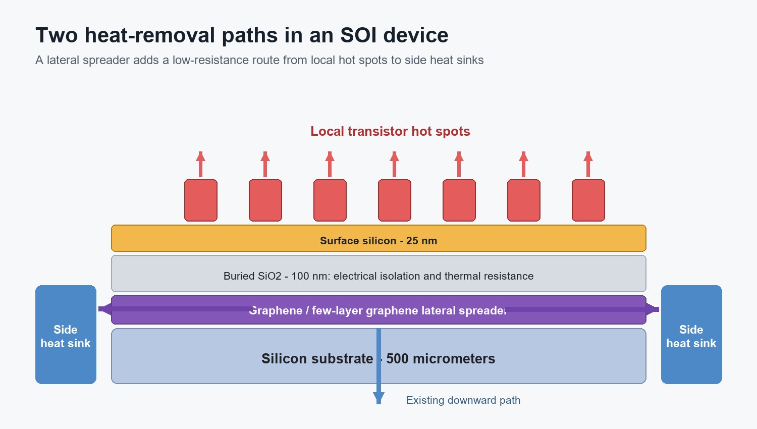
Two heat-removal paths in the modeled SOI stack. Explanatory diagram based on the source discussion; created for this article and not an experimental image.
What the Finite-Element Model Actually Tested
The authors used the finite-element method to solve the steady heat-conduction equation. In plain terms, the device geometry was divided into many small regions, and the calculation balanced the heat generated and conducted through each region until it reached a stable temperature field. This was a numerical feasibility study, not direct thermometry on a fabricated chip. Its value lies in comparing structures under the same assumptions.
The modeled stack included a 500-micrometer silicon substrate, a 100-nanometer buried oxide, and a 25-nanometer surface silicon film. Rectangular transistor channels were separated by 10 micrometers. The bottom of the substrate and both ends of the graphene spreader were held at 300 K, while the other external surfaces were treated as insulated. Heat transport in graphene was assumed to be diffusive because the sheet dimensions were much larger than the phonon mean free path.
Those boundary conditions are not minor details. Holding the ends of the spreader at 300 K represents an effective connection to a cold sink. A graphene sheet placed under a hot spot without a low-resistance destination would merely redistribute energy inside a closed system. Likewise, treating the outer surfaces as insulated removes convection and radiation from the comparison, making the added conduction path easier to isolate but the model cleaner than a complete package.
Why Multiple Hot Spots Change the Value of the Spreader
A single transistor produces a temperature field that decays away from its channel. Add nearby active transistors and those fields begin to overlap. The region between devices no longer returns to the same cool baseline, so each source operates on top of heat contributed by its neighbors. This thermal crosstalk is one reason average chip temperature can conceal a reliability problem.
A lateral spreader helps by collecting energy from several sources and moving it toward the edges. Its benefit can therefore grow with the density of active regions, provided the sheet and its sink connections have enough capacity. That is what the study's comparison between one MOSFET and seven active fingers was designed to reveal.
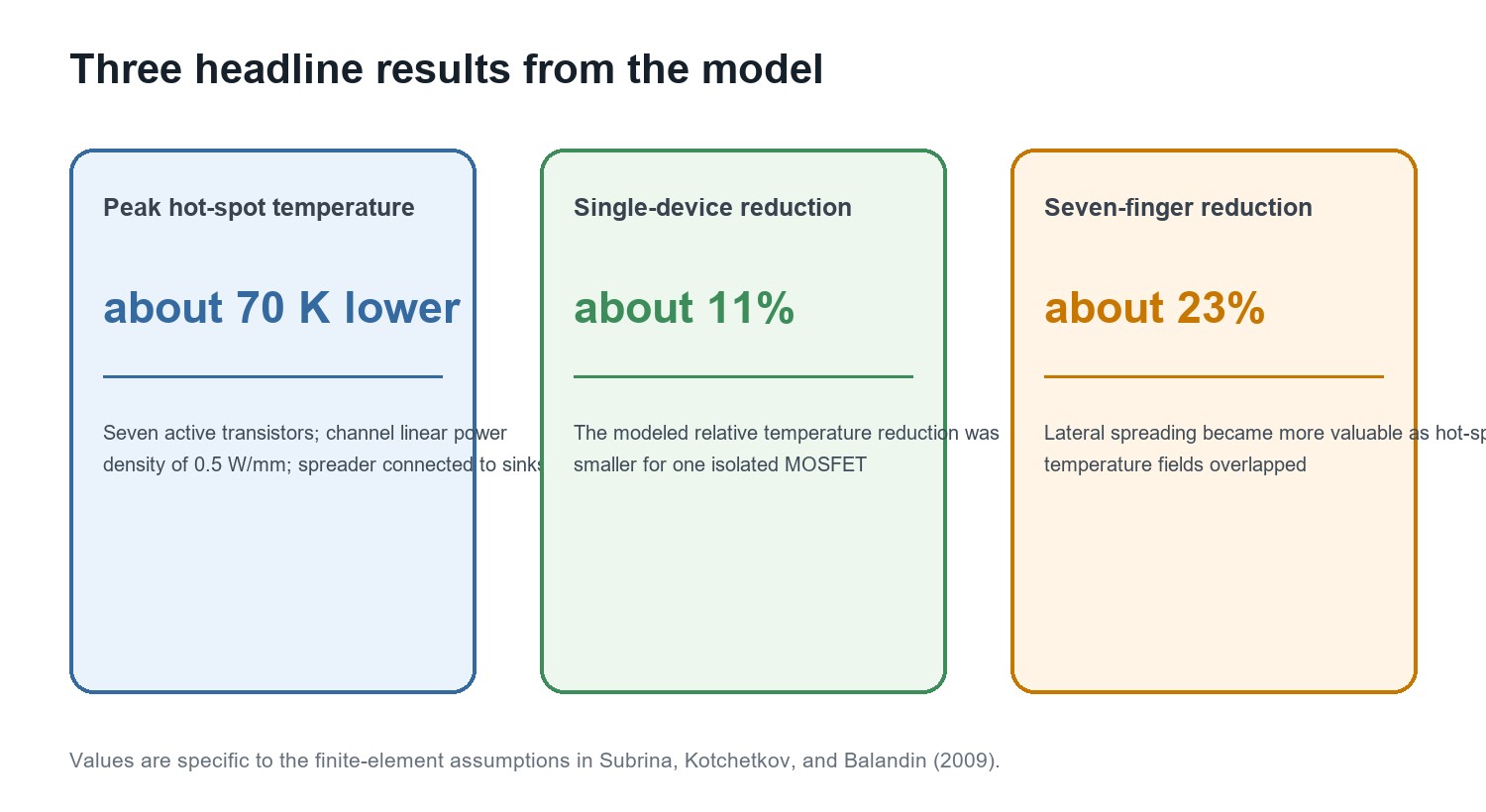
Key results reported by the source study, reorganized from Figures 2 and 3 of Subrina, Kotchetkov, and Balandin (2009). This is a newly drawn explanatory graphic, not an experimental image.
Reading 70 K, 11%, and 23% Without Overpromising
For the seven-transistor case, with a linear power density of 0.5 W/mm in each active channel, adding the heat-spreader layer reduced the modeled maximum hot-spot temperature by about 70 K. In a separate comparison, the reported reduction was about 11% for one MOSFET and about 23% for the seven-finger structure. The larger relative change in the multi-source case supports the idea that lateral spreading becomes more useful when neighboring temperature fields overlap.
These figures are not universal performance guarantees. They depend on the number and spacing of channels, device geometry, substrate thickness, chip dimensions, dissipated power, assumed graphene conductivity, and the ability of the side sinks to remain at the prescribed temperature. A careful interpretation is conditional: under this model and its boundary conditions, the lateral route was strong enough to materially change the peak temperature.
The distinction matters because a temperature reduction can be quoted in several ways. The paper compared simulated profiles with and without the spreader; it did not establish a standardized product benchmark. Applying the same percentage to another chip would require evidence that its heat sources, stack, interfaces, and cold boundaries are comparable.
The Real Obstacles Between a Model and a Manufactured Chip
Design Consideration
Even extremely high in-plane conductivity cannot help if the entrance or exit has a large thermal resistance. Think of it as a high-speed highway fed by a blocked on-ramp: the capacity exists, but the system cannot use it.
The first obstacle is the interface. Heat must leave the transistor region, cross surrounding materials, enter graphene, and then cross another contact into a sink. Even extremely high in-plane conductivity cannot help if the entrance or exit has a large thermal resistance.
The second obstacle is material condition. A large, suspended, high-quality graphene flake is not thermally identical to a processed sheet embedded between oxide and silicon. Edge scattering, contamination, wrinkles, voids, defects, temperature, and fabrication residues can change the effective value. The source paper therefore treated few-layer graphene as a potentially practical compromise. Its intrinsic conductivity may be lower than that of an ideal single layer, but its larger cross-sectional area and mechanical robustness may improve the total path.
The third obstacle is the sink connection. A spreader is an intermediate link, not the final destination. If its ends overlap the sink poorly, travel too far before reaching it, or connect to a sink that heats substantially under load, much of the idealized benefit disappears. Device, spreader, interface, and package need to be modeled as one thermal network.
The Broader Design Lesson
The most durable insight from this study is not that one remarkable material solves chip cooling. It is that hot-spot management can be reframed as heat-path design. The circuit layout determines where heat appears. The dielectric controls cross-plane entry. The spreader determines how quickly heat fans out. The sink and package determine whether that energy can finally leave. Any narrow segment limits the network.
This logic is especially relevant when vertical heat flow is constrained by insulating layers or stacked structures. A lateral route can give a local hot spot another exit and turn a sharp temperature peak into a broader, easier-to-manage profile. The paper also suggested that such an approach could be useful in three-dimensional circuits, but that suggestion should be treated as a design possibility rather than proof of readiness.
Graphene's role here is best understood as a heat-routing element. Its impressive conductivity matters only when geometry, interfaces, and cold-end connections are designed to let the material work. The finite-element results make the route plausible; experiments on real stacks are still needed to measure interface resistance, fabrication variability, and long-term reliability.
FAQ about Graphene Heat Spreaders for SOI Chips
Q: How is a graphene spreader different from a conventional bottom heat sink?
A bottom sink mainly receives heat that travels vertically through the substrate. A graphene spreader first redistributes local heat laterally, then delivers it to side sinks or structures connected to the bottom sink. The two approaches can complement each other; the spreader cannot replace the final heat sink.
Q: Can the reported 70 K reduction be applied to another chip?
No. It came from a specific finite-element model with defined power density, geometry, material properties, and 300 K boundaries. It demonstrates the potential of the heat path, but another device needs its own package-level model and experimental validation.
Q: Why can interface resistance cancel the benefit of high conductivity?
Heat must cross from the oxide into graphene and from graphene into the sink. Small contact area, imperfect bonding, contamination, or vibrational mismatch can restrict those transfers, preventing the high in-plane conductivity from carrying as much heat as the material value suggests.
Conclusion: Graphene Heat Spreaders for SOI Thermal Management
The finite-element study by Subrina, Kotchetkov, and Balandin demonstrates that a lateral graphene layer can meaningfully reduce hot-spot temperatures in SOI structures, especially when multiple active transistors create overlapping thermal fields. However, realizing this benefit in manufactured chips requires solving interface resistance, maintaining material quality through fabrication, and designing effective sink connections. The takeaway is not a universal fix but a design principle: when vertical heat flow is blocked, a well-connected lateral path can make a measurable difference.
Keep Learning
Induction Billet Heating: How to Achieve Uniform Heating
Induction billet heating prepares metal for forging, extrusion, or rolling by generating heat inside the workpiece. For steel billets, reaching the required exit temperature is only part of the task: the temperature distribution from surface to core and along the billet must also suit the forming process. Uniformity depends on how frequency, coil geometry, heat transfer, power distribution, and billet movement work together. This guide focuses on through-heating steel billets, particularly in progress......
How to Upgrade a 3D Printer Heated Bed with a Silicone Heater
If your 3D printer heated bed takes too long to reach temperature, develops uneven heating, or struggles to maintain a stable surface temperature, a silicone heater can be a practical upgrade. Faster warm-up and more uniform heat can improve first-layer consistency and reduce temperature-related printing issues. This guide explains how to identify when a heated-bed upgrade is needed, choose a suitable silicone heater, install it safely, and verify the results. Quick Answer A silicone heater can be a s......
How Graphene and MXene Flake Sensors Detect Force
Key Takeaways Flake networks sense force through microstructural change: Graphene and MXene coatings distribute conduction across overlapping platelets whose contacts shift under stretch or pressure, producing measurable resistance changes. Three mechanisms compete: Crack propagation, flake slippage, and quantum tunnelling each dominate at different deformation levels, giving many sensors multiple sensitivity regions rather than one uniform response. The substrate is an active partner: Elastomers, tex......
Conductive 2D Coatings Are a Matching Problem, Not a Miracle Ink
Key Takeaways Ink is a system, not a material: Conductivity depends on the combined effect of flake chemistry, solvent, additives, substrate, coating method, and post-processing—not on the 2D filler alone. Three carbon routes carry different trade-offs: GNPs demand dispersion engineering, GO shifts effort to a reduction step, and MXenes move the bottleneck to synthesis, storage, and oxidation control. Substrate geometry drives method selection: Spray and blade coating suit flat sheets; dip coating nat......
Graphene Heat Spreader Design: Layers and Interfaces
Key Takeaways Conductivity alone is not enough: A record thermal-conductivity value does not guarantee a cooler chip. Effective thickness, interface resistance, hot-spot geometry, and heat-sink connections all belong to the same thermal path. Few-layer graphene can outperform a single layer in practice: A few-layer sheet provides a larger heat-flow cross section and better tolerates transfer, embedding, and defects, even though its intrinsic conductivity is lower. Interface resistance is the bottlenec......
How Graphene Heat Spreaders Cool SOI Chip Hot Spots
Key Takeaways Buried oxide is a thermal bottleneck: SOI's insulating layer improves electrical isolation but traps heat near transistor channels, creating dangerous hot spots that package-level cooling alone cannot fix. Graphene enables lateral heat routing: Placing graphene or few-layer graphene beneath the buried oxide adds a high-conductivity sideways path, redistributing hot-spot energy toward dedicated sinks without removing any heat itself. Multi-source chips benefit most: Finite-element modelin......