Graphene Heat Spreader Design: Layers and Interfaces
10 min
- The Seductive Simplicity of One Material Number
- Break the Path into Resistances Before Choosing the Material
- Why Thickness Can Compensate for Some Loss in Conductivity
- Why the Model Curves Are Not Purchasing Specifications
- Interface Resistance Is the Narrow Entrance to a Fast Road
- Turn the Paper into a Design Checklist
- FAQ about Graphene Heat Spreader Design
Key Takeaways
Conductivity alone is not enough: A record thermal-conductivity value does not guarantee a cooler chip. Effective thickness, interface resistance, hot-spot geometry, and heat-sink connections all belong to the same thermal path.
Few-layer graphene can outperform a single layer in practice: A few-layer sheet provides a larger heat-flow cross section and better tolerates transfer, embedding, and defects, even though its intrinsic conductivity is lower.
Interface resistance is the bottleneck: Heat must cross from oxide into graphene and from graphene into the sink. Poor bonding, contamination, or vibrational mismatch at these boundaries can cancel the benefit of high in-plane conductivity.
Design the whole network, not just the material: Optimizing a graphene heat spreader means lowering end-to-end thermal resistance while keeping the result manufacturable and stable across the full path from transistor to heat sink.
The Seductive Simplicity of One Material Number
Graphene heat-spreader discussions often begin with a spectacular number: thermal conductivity. If a material can conduct heat far better than silicon dioxide, the intuitive conclusion is that the material with the highest possible conductivity must deliver the best cooling. That conclusion skips the system surrounding the material. Thermal conductivity describes transport within a specimen; it does not say how easily heat enters that specimen, how much cross-sectional area is available, or whether energy can leave at the far end.
Subrina, Kotchetkov, and Balandin explored this distinction in a 2009 finite-element study of lateral graphene spreaders in silicon-on-insulator circuits. Their model placed graphene or few-layer graphene between the buried oxide and silicon substrate, attached the sheet to heat sinks at its ends, and varied both thermal conductivity and the number of atomic planes. Higher conductivity and greater thickness generally lowered the calculated peak temperature, yet the paper argued that a few layers might be more practical than an ideal single layer.
That is not a contradiction. A single layer may offer exceptional intrinsic transport, but a few-layer sheet provides a larger heat-flow cross section and may tolerate transfer, embedding, and local defects more reliably. Engineering performance belongs to the whole path, not to the record value of one isolated sample.
Break the Path into Resistances Before Choosing the Material
From transistor channel to heat sink, energy must pass through several stages. It is generated and concentrated near the active region, crosses the surface silicon and buried oxide, enters the graphene sheet, travels laterally, and finally crosses another interface into a sink. Each stage behaves like a thermal resistance. In a series path, one large resistance can limit the total heat flow even when every other segment is excellent.
The contrast between silicon and oxide illustrates the issue. The paper's model assigned silicon a thermal conductivity of 155 W/(m·K) and silicon dioxide only 1.38 W/(m·K). Graphene can carry heat rapidly along its plane, but the energy must first couple through the low-conductivity region and across the graphene-SiO₂ interface. If that entry is restrictive, raising graphene's conductivity will eventually produce diminishing returns.
The exit matters just as much. A wide sheet with a short, well-bonded overlap to a cool sink is not equivalent to a long sheet touching the sink over a small or contaminated area. Asking only for the conductivity, or k value, leaves out sheet thickness, width, travel distance, contact resistance, and sink temperature—all variables that determine the end-to-end thermal resistance.
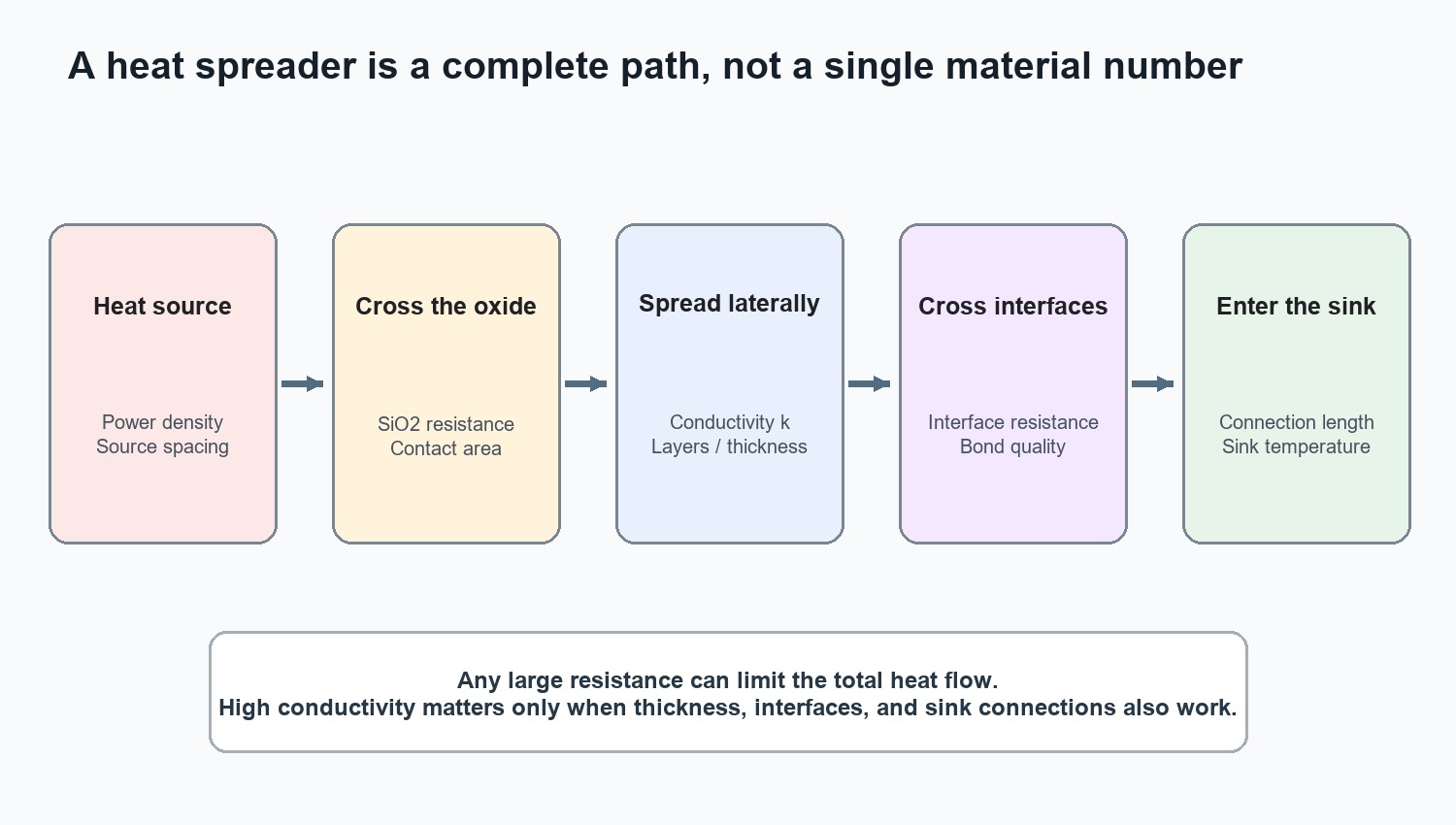
The series thermal path from transistor channel to heat sink. Explanatory diagram based on the source discussion; created for this article and not an experimental image.
Why Thickness Can Compensate for Some Loss in Conductivity
In a simple conduction picture, heat-carrying capacity depends on both thermal conductivity and the cross-sectional area available to the flow. A single graphene layer may have a higher intrinsic in-plane conductivity, but it is extraordinarily thin. Adding atomic planes increases the effective cross section. The conductivity per unit thickness may decline, while the total ability of the sheet to move heat sideways can still increase.
The study varied assumed spreader conductivity from 1,000 to 5,000 W/(m·K) and compared layers containing 1, 10, 20, and 100 atomic planes. Across those modeled cases, increasing conductivity and layer count generally reduced the maximum chip temperature. The authors further suggested that a spreader with roughly 3–10 atomic planes could be effective. That range is a clue from one geometry, not a universal design rule.
Thickness may also improve manufacturability. A perfect, unbroken single atomic layer has little tolerance for local tears, discontinuities, or poor bonding. A few-layer material offers more cross section and can be less sensitive to damage when embedded between oxide and substrate. The trade-off is that its thermal conductivity is expected to fall below ideal graphene and move toward the basal-plane value of bulk graphite, around 2,000 W/(m·K) at room temperature as discussed in the paper.
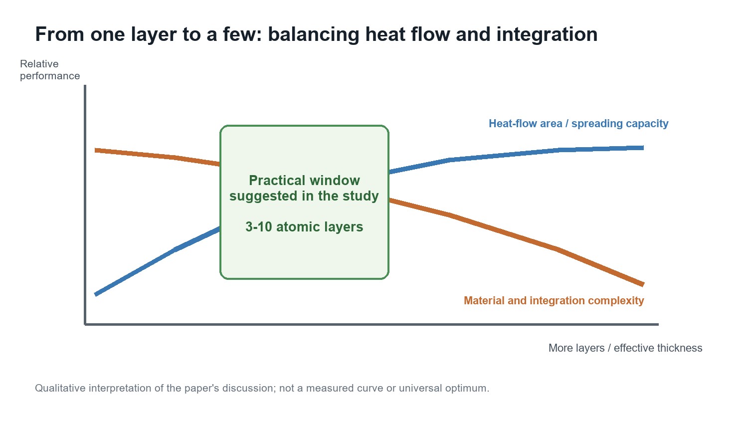
Qualitative balance between heat-flow capacity and integration complexity. Explanatory diagram based on the source discussion; not a measured curve or experimental image.
Why the Model Curves Are Not Purchasing Specifications
Finite-element results are conditional statements. The paper held the bottom heat sink and both ends of the graphene spreader at 300 K, treated the other outer surfaces as insulated, and assumed diffusive heat transport in graphene. Those choices are useful for isolating the effect of the lateral path, but real packages are less orderly. Heat sinks warm under load, interfaces vary across an area, and material conductivity changes with size, temperature, and defects.
The modeled trends remain informative. At a given layer count, higher spreader conductivity lowered the peak temperature; at a given conductivity, thicker spreaders performed better. The curves function as a sensitivity study, showing which levers matter and where gains may continue. Reading one exact temperature from the graph and transferring it to a different chip would ignore geometry, boundary conditions, and uncertainty.
Source layout is another critical variable. The paper reported a larger relative benefit for seven active fingers than for a single MOSFET. That does not make seven a magic number. It indicates that heat-source density and thermal crosstalk can increase the value of a lateral path. A useful test structure must therefore resemble the intended distribution of active devices, not merely measure an isolated sheet.
Interface Resistance Is the Narrow Entrance to a Fast Road
Critical Design Point
Imagine graphene as a high-speed highway. The interfaces are its on-ramp and off-ramp. Heat crossing from silicon dioxide into graphene encounters a boundary between materials whose vibrational behavior differs. Contamination, voids, roughness, wrinkles, and process residue can add further resistance.
At the device scale, these effects are summarized as thermal boundary or interface resistance. The source paper specifically warned that graphene-SiO₂ interface resistance could undermine hot-spot remediation even when lateral conductivity is extremely high. A credible evaluation therefore needs at least three types of data: the effective in-plane conductivity of the embedded spreader, the resistance from the heat-generating stack into the spreader, and the resistance from the spreader into the heat sink. Reporting the first while assuming perfect contacts can make the design look unrealistically strong.
Larger area is not automatically a cure. Extending the spreader can distribute energy over more material, but it also creates more interface area that must be bonded consistently. Wrinkles, voids, or partial delamination can make the effective contact area much smaller than the geometric footprint. Interface uniformity belongs in both process control and thermal modeling.
Turn the Paper into a Design Checklist
-
Map the Heat Sources
Start with the sources, not the total chip power. Record peak power density, source dimensions, spacing, and how many devices operate at once. These variables determine whether temperature fields overlap. Establish a baseline model without the spreader and identify where the largest temperature drops occur to reveal whether the buried oxide, an interface, the substrate, or the package dominates the existing path.
-
Sweep Variables Together
Change spreader conductivity, thickness or layer count, distance to the sink, and interface resistance simultaneously. If the design works only when every interface is ideal, it carries high manufacturing risk. Include the cold boundary explicitly: a side sink is not simply a constant-temperature symbol, but a physical structure with finite size, conductivity, and its own contact resistance.
-
Validate What Fabrication May Change
Measure the embedded material rather than relying only on values from suspended flakes. Inspect bonding and continuity over the whole active area. Test thermal cycling and mechanical stress, because a spreader that performs well immediately after fabrication may change during service. The paper's 3–10-layer suggestion is a reasonable exploration window, but the final choice must come from the actual process and package.
This checklist changes the optimization target. Instead of searching for the highest possible k value, the goal becomes lowering end-to-end thermal resistance while keeping the result manufacturable and stable. High conductivity then serves a system design rather than substituting for one.
FAQ about Graphene Heat Spreader Design
Q: Why might few-layer graphene cool better than a single layer in practice?
Few-layer graphene provides a larger heat-flow cross section and may better tolerate transfer, embedding, and local defects. Even if its intrinsic conductivity is lower than that of ideal single-layer graphene, its total spreading capacity and manufacturing stability can be better.
Q: Is 3-10 layers the best range for every chip?
No. The source paper proposed that range as effective in its particular SOI finite-element model. The real optimum depends on source layout, interface resistance, material quality, distance to the heat sink, fabrication constraints, and package conditions.
Q: What data matter most beyond in-plane conductivity?
Measure the thermal resistance between graphene and adjacent dielectrics, and between graphene and the heat sink. Those interfaces govern how efficiently heat enters and leaves the spreader; without them, a model can substantially overestimate the value of high conductivity.
Conclusion: Designing Graphene Heat Spreaders as a Complete System
Graphene attracts attention because of extraordinary material measurements, but chip thermal management is a network problem. The study supports three measured conclusions within its model: a lateral spreader can substantially lower SOI hot spots; higher conductivity and greater effective thickness generally help; and a few-layer structure may offer a more realistic balance of thermal performance and integration than a single ideal layer.
It also identifies the reasons those gains may shrink in practice: interface resistance, size effects, temperature, defects, sink connection, and device geometry. The simulation did not establish one optimal layer count for every application, and it did not replace package-level experiments. Its contribution is more useful than a universal recipe: it identifies the variables that must be optimized together.
A mature graphene heat-spreader design would therefore report a full thermal-resistance budget, measured interfaces, fabrication tolerances, and validation under realistic loads. Only then does an impressive material property become predictable cooling performance.
Keep Learning
Induction Billet Heating: How to Achieve Uniform Heating
Induction billet heating prepares metal for forging, extrusion, or rolling by generating heat inside the workpiece. For steel billets, reaching the required exit temperature is only part of the task: the temperature distribution from surface to core and along the billet must also suit the forming process. Uniformity depends on how frequency, coil geometry, heat transfer, power distribution, and billet movement work together. This guide focuses on through-heating steel billets, particularly in progress......
How to Upgrade a 3D Printer Heated Bed with a Silicone Heater
If your 3D printer heated bed takes too long to reach temperature, develops uneven heating, or struggles to maintain a stable surface temperature, a silicone heater can be a practical upgrade. Faster warm-up and more uniform heat can improve first-layer consistency and reduce temperature-related printing issues. This guide explains how to identify when a heated-bed upgrade is needed, choose a suitable silicone heater, install it safely, and verify the results. Quick Answer A silicone heater can be a s......
How Graphene and MXene Flake Sensors Detect Force
Key Takeaways Flake networks sense force through microstructural change: Graphene and MXene coatings distribute conduction across overlapping platelets whose contacts shift under stretch or pressure, producing measurable resistance changes. Three mechanisms compete: Crack propagation, flake slippage, and quantum tunnelling each dominate at different deformation levels, giving many sensors multiple sensitivity regions rather than one uniform response. The substrate is an active partner: Elastomers, tex......
Conductive 2D Coatings Are a Matching Problem, Not a Miracle Ink
Key Takeaways Ink is a system, not a material: Conductivity depends on the combined effect of flake chemistry, solvent, additives, substrate, coating method, and post-processing—not on the 2D filler alone. Three carbon routes carry different trade-offs: GNPs demand dispersion engineering, GO shifts effort to a reduction step, and MXenes move the bottleneck to synthesis, storage, and oxidation control. Substrate geometry drives method selection: Spray and blade coating suit flat sheets; dip coating nat......
Graphene Heat Spreader Design: Layers and Interfaces
Key Takeaways Conductivity alone is not enough: A record thermal-conductivity value does not guarantee a cooler chip. Effective thickness, interface resistance, hot-spot geometry, and heat-sink connections all belong to the same thermal path. Few-layer graphene can outperform a single layer in practice: A few-layer sheet provides a larger heat-flow cross section and better tolerates transfer, embedding, and defects, even though its intrinsic conductivity is lower. Interface resistance is the bottlenec......
How Graphene Heat Spreaders Cool SOI Chip Hot Spots
Key Takeaways Buried oxide is a thermal bottleneck: SOI's insulating layer improves electrical isolation but traps heat near transistor channels, creating dangerous hot spots that package-level cooling alone cannot fix. Graphene enables lateral heat routing: Placing graphene or few-layer graphene beneath the buried oxide adds a high-conductivity sideways path, redistributing hot-spot energy toward dedicated sinks without removing any heat itself. Multi-source chips benefit most: Finite-element modelin......