Innovative Applications of Transparent PCBs
14 min
- Transparent PCB Applications
- Key Advantages of Transparent PCBs
- Transparent PCB Materials and Design Considerations
- JLCPCB Transparent FPC Manufacturing Capabilities
- FAQs about Transparent PCBs
- Conclusion: Choosing the Right Transparent PCB
Key Takeaways
- Key Uses: Powers AR glasses, transparent displays, wearables, smart windows, and automotive controls.
- 85% Transmittance: High-transparency PET substrate keeps circuits virtually invisible.
- 200°C SMT Ready: Heat-resistant PET fully supports automated SMT reflow soldering.
- Ultra-Thin: Single-layer (0.14 mm) and double-layer (0.24 mm) options fit curved designs.
- JLCPCB Support: Offers 1/2-layer PET FPCs with ENIG, 3/3 mil trace/space, and fast 4–5 day delivery.
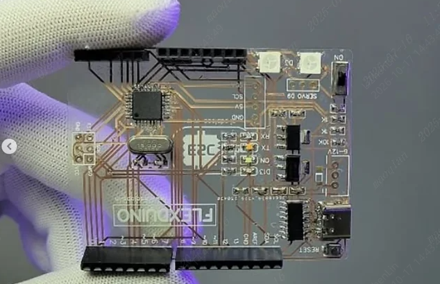
Transparent PCBs combine electrical functionality with visual transparency, creating new design possibilities for electronic products where conventional opaque circuit boards may obstruct light or visibility. Potential applications include optical interfaces, smart wearables, display systems, and integrated lighting.
However, a transparent substrate does not necessarily make the entire circuit assembly transparent. Copper traces, pads, connectors, and mounted components may remain visible, so material selection and circuit layout are important to the final appearance. For applications that require see-through and flexible circuitry, transparent flexible PCBs (FPCs) offer one possible solution, depending on the design requirements and available manufacturing capabilities.
Transparent PCB Applications
1. Transparent PCBs in AR Devices and Smart Glasses
Augmented reality (AR) glasses and heads-up displays require careful integration of electronic circuits, optical components, and user-facing interfaces. Transparent PCBs or transparent flexible circuits may be considered for selected areas where visual obstruction needs to be minimized. Their suitability depends on the required optical clarity, circuit density, and electrical performance.
- Potential system applications include:
- Gesture-sensing interfaces
- Eye-tracking systems
- Heads-up navigation displays
- Transparent display assemblies
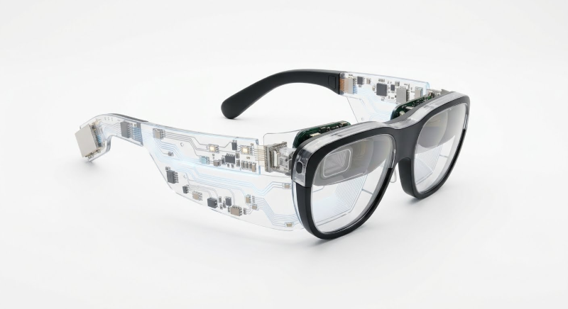
A transparent PCB does not create these functions by itself. Instead, it can serve as part of the electronic interconnection system supporting the sensors, displays, and control electronics. Designers must also consider circuit placement, trace visibility, mechanical stability, and the optical requirements of the complete device.
2. Transparent PCBs in Smartphones and Wearables
Transparent PCBs may be considered in wearable electronics and selected consumer products where circuit visibility and product appearance are important design factors. Flexible circuit structures can also help connect components within compact or curved enclosures.
Possible applications include:
- Wearable accessories and smart jewelry
- Flexible interconnections in compact devices
- Electronic products with transparent housings
- Prototypes exploring see-through product designs
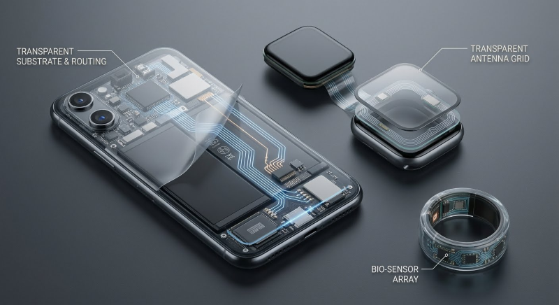
The transparency of a circuit substrate does not make the processor, battery, display, or other components transparent. Designers must evaluate the complete assembly, including component placement, connector visibility, heat generation, and mechanical protection.
For wearable products, material selection and circuit construction should also reflect the expected bending conditions and operating environment. A transparent appearance is only one design consideration; electrical reliability and durability remain essential.
3. Transparent PCBs for Display Systems
Transparent displays combine display technology with optical structures that allow some degree of visibility through the display area. Transparent PCBs or flexible circuits may be used in supporting electronics, depending on the system architecture and the need to limit visual obstruction.
Potential applications include:
- Transparent display systems for retail and digital signage
- Display modules integrated into glass surfaces
- Selected automotive display and heads-up display assemblies

OLED and microLED are display technologies, not guarantees of transparency. The optical properties of a finished display depend on the panel design and its complete optical and electronic structure.
When designing supporting circuits for display systems, engineers should consider the available installation space, interconnection requirements, trace visibility, and the relationship between the circuit layout and the display's viewing area. The final optical performance must be evaluated at the system level rather than inferred from the PCB substrate alone.
4. Transparent PCBs in Medical and Biosensing Devices
Transparent circuit structures may be useful in selected medical and biosensing devices when visual access, compact integration, or a low-profile form factor is important. Their suitability depends on the device architecture, electrical requirements, material compatibility, and applicable safety and regulatory requirements.
Potential areas of application include:
- Transparent or low-profile wearable sensor patches
- Wearable biosensing systems
- Flexible circuits used in ECG and EEG monitoring equipment
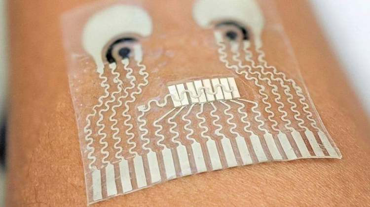
Transparency alone does not establish biocompatibility or suitability for implantation or long-term skin contact. Medical applications require appropriate material validation, electrical safety evaluation, and product-specific testing.
For designers, the priority is to balance the required form factor with electrical performance and the conditions under which the device will be used. Material and manufacturing choices should be validated against the intended application rather than selected on appearance alone.
5. Transparent PCBs in Smart Windows and Solar Systems
Smart windows and transparent solar technologies combine optical materials with electronic control or energy-conversion systems. Transparent PCBs may be used in selected supporting circuits, such as control modules or interconnections, when their structure and environmental requirements are compatible with the application.
Examples include:
- Control electronics for switchable smart-glass systems
- Supporting circuits in building-integrated electronic installations
- Interconnections in selected transparent solar or energy-harvesting systems
The circuit board is only one part of these systems. Light transmission, switching behavior, and energy conversion depend primarily on the relevant glass, coating, cell, and system designs.
When integrating electronics into windows or other exposed surfaces, engineers should consider installation space, temperature variation, moisture exposure, electrical insulation, and maintenance requirements. The circuit construction must be appropriate for the complete operating environment.
6. Transparent PCBs in Automotive Interiors
Transparent or visually unobtrusive circuits may support selected automotive interior concepts where lighting, displays, and touch interfaces are integrated into glass or decorative surfaces.
Potential applications include:
- Interconnections for integrated interior lighting
- Supporting electronics for touch-sensitive control surfaces
- Circuit integration in selected display or console assemblies
Automotive use requires more than an appealing appearance. Designers must evaluate temperature variation, vibration, moisture exposure, electrical loading, mechanical protection, and the applicable automotive qualification requirements for the complete assembly.
The design should also account for serviceability and the interaction between circuit structures, touch sensors, lighting elements, and decorative materials. Transparency may support the desired appearance, but it does not replace the reliability and validation requirements of automotive electronics.
7. Transparent PCBs in Fashion Tech and Smart Textiles
Transparent and flexible circuit structures can be explored in fashion technology and wearable products where appearance and compact integration are important. Depending on the design, they may support lighting, sensing, or interactive electronic features.
Potential applications include:
- Light-emitting garments with integrated electronics
- Electronic accessories
- Wearable products with interactive features
The visibility of traces, connectors, and components depends on the circuit design and materials. In textile applications, mechanical strain, repeated movement, moisture, and the method used to attach or protect the circuit must also be considered.
A flexible circuit must be matched to the way a garment or accessory moves during use. Designers should evaluate bending and strain points, connection methods, and protective structures early in the development process to reduce the risk of damage during repeated use.
8. Transparent PCBs in Lighting Systems
Transparent PCBs may be considered in lighting products where circuit visibility or the integration of electronics into a clear enclosure is an important design factor. The actual lighting effect depends on the light source, optical components, enclosure, and circuit layout.
Potential applications include:
- Lighting integrated into transparent product housings
- Decorative lighting systems
- Retail displays with integrated electronic controls
A transparent circuit substrate does not automatically provide uniform light diffusion. Designers should evaluate optical performance and electrical requirements at the complete product level.
For products with visible circuitry, component placement and trace routing can also affect the finished appearance. The design should balance the desired visual effect with current requirements, thermal behavior, electrical spacing, and the space needed for connectors and other components.
Key Advantages of Transparent PCBs
Transparent PCBs can offer several design advantages when optical access and visual integration are important. The benefits depend on the substrate, circuit construction, and requirements of the finished product.
Visual Integration: Transparent substrates can reduce the visual obstruction caused by conventional opaque board materials in suitable designs.
Flexible Design Options: Transparent flexible PCBs can support curved or space-constrained assemblies when the substrate and circuit structure meet the mechanical requirements.
Compact Integration: Thin circuit structures may help designers integrate electronics into products with limited space.
Optical-System Integration: Transparent circuits may be useful in selected display, sensing, and lighting assemblies where the circuit structure must be considered alongside optical components.
Product Differentiation: Visible or partially transparent electronics can create distinctive product aesthetics, depending on the overall design.
These advantages should be evaluated against the electrical, mechanical, thermal, and optical requirements of each application. Transparency alone does not guarantee better performance, lower weight, greater flexibility, or improved reliability.
Transparent PCB Materials and Design Considerations
Selecting a transparent PCB involves more than choosing a clear substrate. Designers must evaluate material properties, circuit visibility, electrical requirements, mechanical constraints, and compatibility with the intended manufacturing and assembly processes.
Substrate Materials and Transparency
The substrate is an important factor in determining the optical appearance and mechanical behavior of a transparent PCB. Transparent polyethylene terephthalate (PET) is used in certain flexible circuit constructions, while conventional flexible PCBs commonly use polyimide (PI).
These materials should not be treated as interchangeable. Their thermal behavior, mechanical properties, and manufacturing compatibility differ, so material selection should reflect the product's optical requirements, operating environment, assembly process, and expected service life.
A transparent substrate alone does not guarantee that the completed circuit will appear fully transparent. Conductive traces, pads, coverlay, connectors, and mounted components can all affect the appearance of the finished assembly.
| Property | Transparent PET Substrate (JLCPCB Option) | Standard Yellow Polyimide (PI) | Transparent Polyimide (PI) | Rigid Glass / PMMA Substrates |
|---|---|---|---|---|
| Optical Transmittance | High (80% - 85%) | Very Low (Opaque Yellow/Amber) | High (85% - 90%) | Extremely High (>92%) |
| Flexibility & Bending | Excellent (Supports dynamic & static bending) | Excellent | Excellent | Rigid / Non-flexible (Cannot bend) |
| Thermal Resistance | Moderate-High (Rated up to 200°C) | Extremely High (>300°C) | High (260°C - 300°C) | High (Glass) / Low (PMMA <90°C) |
| SMT Reflow Support | Compatible (Requires high-temp PET) | Fully Compatible | Compatible | Glass Compatible / PMMA Non-compatible |
| Material Cost | Highly Cost-Effective | Moderate | Expensive | High (Complex fabrication) |
| Primary Uses | Wearables, Consumer Electronics, Transparent Displays, Smart Windows | Standard Industrial/Military FPCs (Non-transparent) | High-end Aerospace, Micro-displays | Rigid Glass Architecture, Automotive Large Displays |
Trace Visibility and Optical Requirements
In many transparent PCB designs, the substrate is transparent while copper traces, pads, and mounted components remain visible. Their size, density, position, and contrast against the background influence the appearance of the finished assembly.
Designers should identify the areas where visibility matters most and consider:
Trace routing and copper coverage
Component and connector placement
The viewing angle and background
The required level of optical transparency
The appearance of exposed pads and protective layers
If an application requires the conductive traces themselves to be transparent, the project may need a different conductive-material system rather than a conventional copper-based FPC. This is an important distinction when defining the technical requirements for a transparent circuit.
Electrical and Mechanical Design
Transparent PCB design must satisfy electrical and mechanical requirements as well as optical goals. Trace width and spacing, current requirements, connector design, bending conditions, and component placement should be evaluated together.
For flexible circuits, designers should distinguish between static bending during installation and repeated dynamic bending during operation. A design suitable for a one-time bend may not be reliable under repeated movement. Bending areas, transition zones, and component-support requirements should therefore be considered early in the design process.
Other considerations include:
Electrical performance: Confirm that the circuit meets current, voltage, and signal requirements.
Mechanical protection: Identify areas that may experience impact, friction, or repeated movement.
Thermal conditions: Check whether the substrate and complete assembly can tolerate the expected operating and assembly temperatures.
Connection reliability: Ensure that connectors, solder joints, and component interfaces suit the product's operating conditions.
The appropriate design depends on the intended application. A transparent circuit used in a stationary display enclosure may have very different requirements from one incorporated into a frequently flexed wearable device.
Manufacturing and Assembly Compatibility
A transparent PCB design should be checked against the manufacturer's available materials, layer structures, thicknesses, and design rules before fabrication. Assembly requirements also matter: the substrate and completed stack-up must be compatible with the intended soldering process and mounted components.
Before ordering, designers should confirm the supported construction and review the design files for manufacturability. For applications with strict optical requirements, the finished assembly should also be evaluated for trace visibility, surface appearance, and performance under the intended operating conditions.
It is particularly important to confirm that a manufacturer's advertised specifications apply to the exact transparent PCB construction being considered. Capabilities for conventional flexible PCBs do not automatically apply to every transparent FPC configuration.
JLCPCB Transparent FPC Manufacturing Capabilities
When selecting a manufacturing partner for a transparent PCB project, designers should confirm the available substrate, layer count, finished thickness, and design constraints before placing an order.
JLCPCB's published flexible PCB capabilities include transparent FPC configurations using 36 μm PET substrate. The listed options include single-layer and double-layer constructions, with finished thicknesses of 0.14 mm and 0.24 mm, respectively. These specifications apply to the listed transparent FPC configurations and should not be interpreted as support for every type of transparent rigid PCB or multilayer transparent circuit.
JLCPCB Transparent FPC Specifications
| Specification Parameter | JLCPCB Published Capability |
|---|---|
| Substrate Material | High-Transparency, High-Temp Resistant PET |
| Base Substrate Thickness | 36 μm |
| Optical Transmittance | Up to 85% |
| Supported Layer Count | Single-layer, Double-layer |
| Finished Board Thickness | Single-layer: ~0.14 mm; Double-layer: ~0.24 mm |
| Min. Trace Width / Space | 12µm copper: 3/3 mil (0.075mm); 18µm copper: 3.5/3.5 mil; 35µm copper: 4/4 mil |
| Coverlay Structure | Transparent PET Coverlay (25 µm PET + 25 µm Adhesive) |
| Surface Finish | Electroless Nickel Immersion Gold (ENIG, 1u" / 2u") |
| Thermal & SMT Assembly | Heat resistant up to 200°C; Fully compatible with automated SMT reflow |
| Outline Processing & Tolerance | High-precision Laser Cutting (Tolerance: ±0.05 mm) |
| Stiffener Options | Transparent PI / FR4 stiffeners supported for connector assembly |
Source: JLCPCB's official Flexible PCB Capabilities page. Specifications should be reconfirmed before ordering.
These configurations may be suitable for projects that require flexible circuitry with a transparent substrate, provided the design meets the available manufacturing requirements. Designers should verify that the selected construction satisfies the optical, electrical, mechanical, and assembly requirements of the intended product.
Before placing an order, review the manufacturer's current design rules and confirm any requirements that fall outside the published specifications. This helps identify potential compatibility issues before fabrication.
FAQs about Transparent PCBs
Q: What are transparent PCBs made of?
Transparent PCBs are mainly made of high-transparency PET or transparent PI substrates. The electrical traces use ultra-thin copper layers or transparent conductive materials to transmit signals.
Q: Can transparent PCBs undergo standard SMT reflow soldering?
Yes. Modern transparent FPCs use heat-resistant PET substrates that tolerate temperatures up to 200 degrees Celsius, making them fully compatible with automated SMT assembly.
Q: Are the copper traces on a transparent PCB completely invisible?
Standard copper traces are extremely thin but remain slightly visible up close. Using narrow line widths like 3 mil minimizes trace visibility and keeps the board visually clean.
Q: What is the light transmittance of JLCPCB transparent FPCs?
JLCPCB transparent FPCs achieve a light transmittance of up to 85 percent in clear substrate areas, which is ideal for displays and optical devices.
Q: What layer counts and thicknesses are supported for transparent FPCs?
JLCPCB supports 1-layer and 2-layer transparent FPCs using a 36 micron PET base. The finished thickness is about 0.14 mm for 1-layer and 0.24 mm for 2-layer boards.
Conclusion: Choosing the Right Transparent PCB
Transparent PCBs offer design possibilities for electronic products that require visual integration, compact circuitry, or flexible interconnections. Potential applications span wearable electronics, display systems, lighting products, and selected sensing or control assemblies.
However, selecting the right solution involves more than choosing a transparent substrate. Optical requirements, trace visibility, electrical performance, mechanical constraints, and assembly compatibility must all be considered. The final performance depends on the complete circuit and product design, not transparency alone.
For projects that require transparent flexible circuitry, JLCPCB offers published single-layer and double-layer transparent FPC configurations using 36 μm PET substrate. Review the available specifications and design requirements to determine whether the supported construction fits your project.
Popular Articles
• Choosing the Right Bend Radius for Durable Flexible PCBs
• Flexible Meets Durable: Understanding Rigid-Flex PCB Technology
• PCB Stiffeners: An Essential Requirement for Flexible Circuits
• The Ultimate Guide to Flexible PCB: Types, Design, and Applications
• 45 Must-Know Flex PCB Design Tips You Can't Afford to Miss!
Keep Learning
Innovative Applications of Transparent PCBs
Key Takeaways Key Uses: Powers AR glasses, transparent displays, wearables, smart windows, and automotive controls. 85% Transmittance: High-transparency PET substrate keeps circuits virtually invisible. 200°C SMT Ready: Heat-resistant PET fully supports automated SMT reflow soldering. Ultra-Thin: Single-layer (0.14 mm) and double-layer (0.24 mm) options fit curved designs. JLCPCB Support: Offers 1/2-layer PET FPCs with ENIG, 3/3 mil trace/space, and fast 4–5 day delivery. Transparent PCBs combine elec......
Choosing the Right Bend Radius for Durable Flexible PCBs
Key Takeaways Mastering the bend radius is essential for reliable flexible PCB design. Following IPC-2223 guidelines, maintain a minimum of 6× total thickness for static bends and 100× for dynamic applications, while using thinner RA copper, adhesiveless polyimide, staggered traces, and cross-hatched patterns in flex zones. Proper material selection, layer stackup optimization, and adequate clearance from stiffeners can dramatically extend flex life and prevent premature trace cracking or delamination......
Flex PCB Stackup Design Guide: Layers, Materials & Reliability
Key Takeaways A reliable flex PCB starts with the right stackup design. The layer structure, material selection, and copper arrangement directly affect flexibility, bend life, electrical performance, and manufacturing reliability. This guide explains single-sided, double-sided, and multilayer flex PCB stackups, including polyimide materials, coverlay, copper types, and key design considerations for creating durable flexible circuits with JLCPCB. Did you ever wonder how a foldable phone can last for 20......
Flexible Meets Durable: Understanding Rigid-Flex PCB Technology
In the rapidly evolving world of electronics, the demand for smaller, more reliable, and more versatile devices continues to grow. To meet these demands, engineers and designers are increasingly turning to Rigid-Flex PCBs. The circuit boards combine rigid and flexible substrates into a single interconnected structure. This combination allows for complex designs that can bend and flex in specific areas while maintaining rigidity in others. To manufacture rigid flex PCBs, IPC offers advice and best prac......
PCB Stiffeners: An Essential Requirement for Flexible Circuits
A printed circuit board stiffener plays an important role when it comes to offering mechanical support to a PCB. They are particularly helpful for flexible circuit boards, that given their name, are flexible and in need of stiffness in certain places. Stiffeners are particularly required when components are placed in a flex zone & the weight of these components stresses the flex material. These components provide a rigid connection from the flexible portion to the solid board. This solidity makes appl......
The Ultimate Guide to Flexible PCB: Types, Design, and Applications
Key Takeaways JLCPCB 1–4 Layer Flex PCB: Supports 1 to 4-layer FPCs with polyimide (PI) substrates and trace/space down to 3/3 mil. Stiffener Selection: Use PI (0.1–0.25mm) for ZIF connectors, FR4 (0.1–1.6mm) for SMT support, and Stainless Steel (0.1–0.3mm) for high rigidity. Layout Optimization: Use cross-hatched copper ground planes and stagger 2-layer traces to eliminate the "I-Beam effect." Surface & Protection: Combine Immersion Gold (ENIG 1u"/2u") for SMT planarity with flex coverlay to protect ......