
DFM and DFA Guidelines for PCB Assembly: Key Design Rules to Prevent Errors and Improve Manufacturability
8 min
- Key Design for Manufacturing (DFM) Rules to Ensure Assembly-Ready PCB Designs
- Design for Assembly (DFA) Rules That Ensure Efficient and Accurate PCB Assembly
- How to Use Automated DFM Tools for Faster, Error-Free PCB Design
- Conclusion
- FAQs
Design for Manufacturing (DFM) is the critical practice of designing a product for ease of manufacturing. In the world of electronics, it is the bridge between a theoretical circuit schematic in your EDA software and a physically producible, reliable PCBA. Integrating DFM principles from the very beginning of your design process is the single most effective way to prevent costly production holds, frustrating board respins, and catastrophic assembly failures.
Think of DFM as a conversation between you, the designer, and the manufacturing equipment. By adhering to DFM rules, you ensure your PCB design "speaks the language" of the fabrication and assembly machines. Fortunately, modern PCB manufacturing and assembly partners like JLCPCB make this process easier with advanced automation tools. JLCPCB’s free, instant DFM analysis tool automatically checks your design files for potential issues before you place a PCB/PCBA order.
Key Design for Manufacturing (DFM) Rules to Ensure Assembly-Ready PCB Designs
The first section of Design for Manufacturing (DFM) considers the raw PCB, but every action you take on it has a direct effect on the finished custom PCBA. These checks help ensure the PCB can be manufactured with reliable quality for assembly.
● Trace Width and Spacing: This is the most fundamental check in DFM. If you violate a manufacturer's minimum trace/space guidelines, you run the risk of shorts on the bare board and can also damage the PCB assembly. Inconsistent trace widths can result in impedance discontinuities, and violated spacing can lead to solder bridging between either pads or traces while passing through the reflow profile. Always design with your manufacturer's standard capabilities (i.e., manufactured 5 mil trace/space at JLCPCB) for the best assembly yield.
● PCB Via Specifications (Annular Ring & Drill Size): The “annular ring” is defined as the ring of copper that surrounds a drilled via. A missing or insufficient annular ring can cause a via to become disconnected from its trace, creating an open circuit on the completed PCBA. In addition, a strong annular ring is also essential for through-hole components whose solder joint integrity must be sufficiently robust to withstand torque and stresses without becoming loose.
● Copper-to-Board-Edge Clearance: Keeping copper a safe distance from the board's edge is critical for PCB assembly reliability. During depanelization, exposed copper can lead to immediate shorts. Over the lifetime of the product, it also creates a failure point, as moisture or debris can cause shorts that are difficult to debug on a fully assembled board.
● Solder Mask and Paste Mask Expansion: These layers are exclusively for the benefit of the PCB assembly process. The solder mask "bridge" between fine-pitch IC pads is essential for preventing solder shorts during assembly. The paste mask openings must be correctly sized to deposit the exact amount of solder paste needed for a good joint—too little results in a weak connection, while too much causes shorts.
Essential DFM checks for a custom PCBA, highlighting trace clearance, via annular ring, and solder mask bridge.
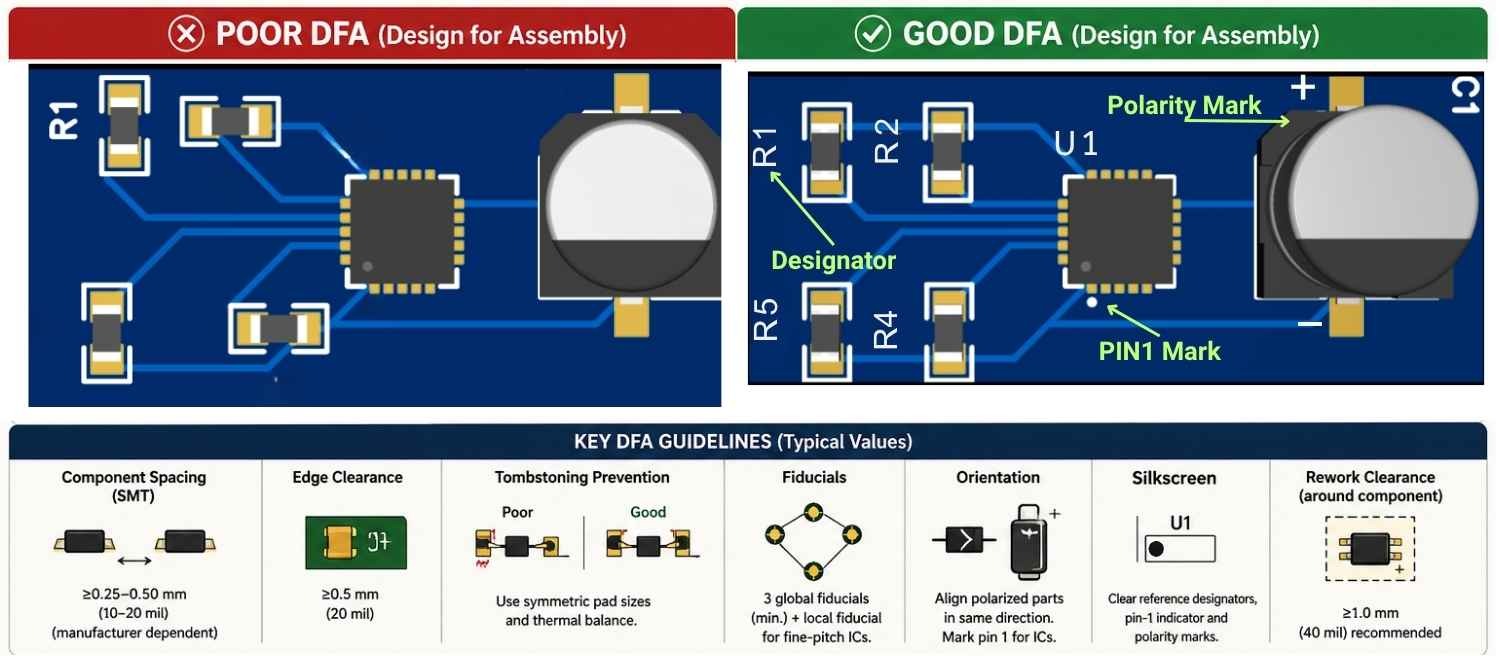
Design for Assembly (DFA) Rules That Ensure Efficient and Accurate PCB Assembly
Design for Assembly (DFA) is a subset of Design for Manufacturing (DFM) that focuses squarely on making the PCB assembly process efficient and error-free.
● Component Clearances: Pick-and-place machines need physical space to function. If components are placed too close together, the machine may hit an already-placed component with the nozzle and either disrupt the assembly or damage one of the components. Clearances are also critical for automated optical inspection (AOI) and any additional manual rework of the assembled PCB.
● Footprint or Land Pattern Verification: This is one of the most critical DFM items for the success of a PCBA. If the footprint does not match up, meaning that the pads on the PCB do not match up with the leads of the component, then PCB assembly becomes impossible. This is a very common mistake that is completely avoidable and leads to a full board respin, which wastes a lot of time and money.
● Fiducial Marks: Fiducials serve as the assembly machine's eyes. These small copper targets are essential to the machine's vision system so it can accurately find the board position. The machine cannot place components accurately - especially fine-pitch parts - without abdicating fiducials, which can result in a failed PCBA run.
● Component Orientation and Polarity: Proper application of silkscreen markings is critical to preventing one of the most detrimental PCBA errors: incorrect component orientation. An improperly oriented polarized capacitor or integrated circuit can experience immediate failure upon power application and may induce secondary damage to adjacent circuitry. Silkscreen indicators provide essential visual cues for assembly technicians, ensuring that each component is placed with the correct polarity and orientation as defined by the design specifications.
How to Use Automated DFM Tools for Faster, Error-Free PCB Design
Manually checking each DFM rule across a complex designed board is tedious and highly error-prone. The modern, efficient approach is to use an automated tool, like the one provided by JLCPCB called JLCDFM.
The Process with JLCDFM:
1. In your preferred EDA software (EasyEDA, KiCad, Altium, Eagle, etc.) simply export the manufacturing files. You will need the Gerber files (Harsh C) for each layer (copper and technical) and the Excellon drill files for the hole information.
2. Package all of these files into a single .zip archive.
3. Visit the JLCPCB DFM tool page and simply upload your .zip file.
The tool will process your files in a few seconds and generate a detailed and interactive report. Any potential problems will be flagged by visually marking them on a rendered image of your layout, making it incredibly easy to find out exactly "where" the problem lies, so you can go back to your design software and fix it.
| Error Type | Example Violation | Why It's a Problem |
|---|---|---|
| Spacing Violation | Trace-to-trace clearance is 3 mil (manufacturer min is 4 mil) | High risk of short circuits during etching. |
| Annular Ring | Ring width is below 1 mil on several vias. | Vias may become disconnected from traces. |
| Solder Mask | No solder mask bridge between 0.4mm pitch IC pads. | High probability of solder bridging and shorts. |
| Open/Short | A trace appears to be shorted to a copper pour. | The board will not function electrically. |
Conclusion
Design for Manufacturing (DFM) shouldn't be described as an "expert" step you consider only for high-volume production. DFM is an essential part of the electronics design process for everyone, from hobbyists to experienced professionals. Choosing to engage in DFM means you will reduce costs as you will lower the probability of a board re-spin, you will get a faster product turnaround by preventing production holds, and you will build a more reliable, robust final product.
Approach the use of a free DFM tool, like JLCDFM, as more than just a final check, but as a process of continuous learning. By running your PCB design through this tool, you will undoubtedly learn about manufacturing constraints that you might not have otherwise considered. Make this the final, must-complete step in your PCB design workflow before you consider placing any custom PCBA order.
FAQs
1. What is the difference between my EDA's DRC and a DFM check?
Your Design Rule Check (DRC) verifies your design against the rules you set up in your software. A DFM check verifies your design against the specific capabilities and rules of the manufacturer (e.g., JLCPCB). The DFM check is what ultimately matters, as it confirms if your board can actually be built on the manufacturer’s equipment.
2. Is the JLCPCB DFM tool free to use?
Yes, it is a completely free service. You can upload and check your designs as many times as you need to iterate and improve them, all without any obligation to place a PCB/PCBA order.
3. Does DFM only matter for high-volume PCB production?
Not at all. DFM is arguably even more critical for prototypes and low-volume runs. A single failed board in a batch of five is a 20% failure rate, which can completely derail a project. For hobbyists and students, a board that fails due to a preventable DFM error means wasted time and money. DFM principles ensure that even a single prototype has the highest possible chance of success.
4. Can the DFM tool check if I used the correct component footprint?
No. An automated DFM tool is brilliant at finding physical manufacturability issues (like clearances, trace widths, and annular rings), but it cannot know the designer's intent. It can't verify that the footprint you chose for a specific part number is dimensionally correct. That critical verification step remains the responsibility of the designer.
Popular Articles
• How to Create a Bluetooth-Controlled Car With Arduino: A Step-by-Step Guide
• How to Design and Assemble a Reliable ESP32 Module PCB on a 2-Layer Board
• The Ultimate Guide to Relay Symbol: Coil, Contacts, Diagrams, and Circuit Applications
• How to Identify SMD LED Polarity: Markings, Testing, and PCB Tips
• The Ultimate Guide to PCBA: Process,Types and Techniques for the Electronics Enthusiast
Keep Learning
How to Design an ESP32-S3 Development Board from Scratch: A 4-Layer PCB Design Tutorial
Designing your own ESP32-S3 development board gives you complete control over your hardware architecture while preparing your IoT projects for commercial production. Instead of relying on bulkier, off-the-shelf boards, building a custom design allows you to optimize the board space, expose only the required GPIO pins, and integrate peripherals directly onto a single substrate. In this tutorial, we will design a 4-layer ESP32-S3 development board from scratch. We will walk through the entire hardware d......
Arduino LED Driver Tutorial: Control More LEDs with 74HC595 and MAX7219
Arduino GPIO pins run out quickly in larger LED projects. By utilizing dedicated LED drivers and expansion ICs, you can drastically reduce pin usage, eliminate processor-heavy multiplexing loops, and simplify display wiring. In this guide, you will learn the operational architecture, wiring configurations, cascading techniques, and optimization strategies for the 74HC595 shift register and the MAX7219 LED driver. Why Arduino Projects Need LED Driver ICs Arduino GPIO and Current Limitations An ATmega32......
How to Create a Bluetooth-Controlled Car With Arduino: A Step-by-Step Guide
This tutorial walks through the complete engineering and implementation of a two-wheel Bluetooth RC car with an Arduino Nano module on a specially designed PCBA (Printed Circuit Board Assembly). While many hobbyists start by wiring motors and Bluetooth modules with jumper cables on a breadboard, this approach is prone to disconnection and signal noise. This guide upgrades that process by teaching you how to design a professional mainboard. Key Design Features Controller: Arduino Nano used as a plug-in......
Fiducial Marks in PCB and SMT Assembly: A Complete Guide to Accuracy and Design Rules
Modern Printed Circuit Boards (PCBs) are complex, integrating high-density components like 0.4mm pitch Ball Grid Arrays (BGAs), 0201 passives, and fine-pitch Quad Flat No-Lead (QFN) packages. In this advanced manufacturing environment, achieving placement accuracy measured in micrometers is crucial. A significant challenge in automated manufacturing is how pick-and-place machines, which handle thousands of components per hour, precisely locate the PCB. A board on a conveyor system is never in the perf......
Alternating Current vs Direct Current (AC vs DC): What's the Difference?
Electric current flows in two primary forms: alternating current (AC) and direct current (DC). AC periodically reverses direction, while DC flows steadily in one direction. AC powers the industrial and residential electrical grids, while DC powers batteries, electric vehicles, and nearly all modern consumer electronics. Understanding the core differences between AC and DC matters when designing power supplies, selecting electronic components, or laying out printed circuit boards (PCBs). This guide com......
Arduino LED Multiplexing Tutorial: Control More LEDs with Fewer Pins
The Arduino Uno is a powerful tool for prototyping, but driving multiple LEDs directly quickly exhausts its 20 GPIO pins and its 200 mA absolute maximum package current limit. To bypass these hardware bottlenecks, engineers and hobbyists use LED multiplexing to scale display outputs efficiently without upgrading the microcontroller. In this guide, you will learn the core principles of LED matrix scanning, Charlieplexing, refresh timing, ghosting fixes, and practical Arduino code without relying on any......