
Mastering BT Resin Packaging: Technical Insights & JLCPCB Capabilities
12 min
- What is BT Resin? Understanding the Chemical Makeup and Core Properties
- Critical Applications: Where BT Resin Boards Form the Backbone
- Manufacturing Challenges of BT Resin PCBs
- How JLCPCB Delivers Excellence in BT Resin and High-Reliability PCB Fabrication
- FAQ about BT Resin Packaging
- Conclusion: Accelerate Your BT Resin Designs with JLCPCB
Key Takeaways
- BT resin is a high-performance thermoset polymer with Tg of 180°C–210°C, ultra-low Dk/Df, and under 0.05% moisture absorption — essential for advanced IC packaging substrates (BGA, CSP, SiP).
- Its dense cross-linked structure provides superior resistance to electromigration, dendrite growth, and chemical degradation, making it ideal for fine-pitch, high-reliability applications.
- Manufacturing BT resin PCBs requires specialized diamond-coated drilling, UV/CO2 hybrid laser systems, and precise chemical desmear to avoid micro-fracturing and smear.
- Surface finishes must be ENIG or ENEPIG — standard HASL is unsuitable for the flatness and coplanarity required by semiconductor bonding.
- JLCPCB offers automated LDI, hybrid laser drilling, AOI/AXI inspection, and seamless prototype-to-mass-production scaling for BT resin and high-reliability PCBs.
The global semiconductor shift toward extreme miniaturization, high-frequency signals, and dense 3D heterogeneous architectures has pushed traditional substrate materials to their physical limits. While standard FR4 remains the workhorse for conventional electronics, next-generation Integrated Circuit (IC) packaging demands a substrate with superior dimensional stability, exceptional thermal endurance, and minimal signal loss.
Enter Bismaleimide-Triazine resin, universally known as BT resin. As the foundational chemistry behind elite IC substrates (such as BGA, CSP, and SiP), BT resin bridges the gap between raw silicon dies and traditional systems-level PCBs. However, harnessing this high-performance thermoset polymer requires more than just high-grade sourcing—it mandates highly precise, automated fabrication infrastructure.
What is BT Resin? Understanding the Chemical Makeup and Core Properties
To maximize the performance of an advanced package, an engineer must understand the fundamental material science of BT resin. Unlike standard epoxy systems, BT resin is formed through the co-polymerization of bismaleimide and triazine chloride derivatives (cyanate esters). This reaction yields a highly cross-linked, dense molecular structure that retains mechanical integrity under environmental conditions that would cause standard laminates to degrade.
The Chemistry Behind Bismaleimide-Triazine (BT)
The aromatic rings and alternating nitrogen-carbon structures inherent to the triazine network introduce tremendous structural rigidity. Simultaneously, the imide rings contribute exceptional thermal stability and chemical resistance.
Chemical Reaction Pathway
-
Monomer Combination
Bismaleimide Monomer combines with Triazine Cyanate Ester.
-
High-Temperature Co-Polymerization
Forms a dense, highly cross-linked polymeric network.
-
Dual-Axis Stability
Boosts thermal power (high Tg, low CTE) and electrical purity (low Dk/Df, anti-electromigration).
Why This Matters for Fine-Pitch Layouts
- High Resistance to Electromigration: Prevents the physical displacement of metal atoms caused by dense electric fields between fine-pitch traces.
- Dendrite Suppression: The chemical matrix inherently inhibits copper dendrite growth under biased voltage, eliminating a major cause of catastrophic short circuits.
- Chemical Inertness: Resists degradation from harsh stripping chemicals and flux residues used during flip-chip assembly.
Key Thermal Properties: High Tg and Low CTE
In IC packaging, structural failure often stems from mismatched coefficients of thermal expansion (CTE) between the silicon die (around 2.6 ppm/°C), the substrate material, and the motherboard (around 16 ppm/°C). BT resin addresses this issue by maintaining an exceptionally high glass transition temperature (Tg) of 180°C to over 210°C, depending on individual formulations.
Because the material remains structurally stable beyond standard reflow temperatures, its Z-axis CTE remains tightly restricted. This minimal Z-axis expansion prevents microvia cracking and pad lifting during multi-cycle lead-free reflow profiles and subsequent ultrasonic wire bonding processes.
Electrical Performance: Low Dk and Df for High-Speed Signals
For high-speed digital communications, millimeter-wave radar, and optoelectronics, dielectric loss directly dictates signal range and power efficiency. BT resin provides a highly stable dielectric constant (Dk) and an ultra-low dissipation factor (Df) across wide frequency bands.
Furthermore, its ultra-low moisture absorption rate (less than 0.05%) ensures that these electrical parameters remain completely stable even when exposed to high-humidity deployment environments, preventing impedance shifts in high-speed transmission lines.
| Material Property | Standard FR4 | Premium High-Tg FR4 | Advanced BT Resin |
|---|---|---|---|
| Glass Transition Temp (Tg) | 130°C to 140°C | 170°C to 180°C | 180°C to 210°C |
| Decomposition Temp (Td) | 300°C | 340°C | 350°C to 410°C |
| Z-Axis CTE (Before Tg) | 50 to 60 ppm/°C | 40 to 45 ppm/°C | 25 to 30 ppm/°C |
| Dielectric Constant (Dk @ 1GHz) | 4.2 to 4.7 | 3.9 to 4.3 | 3.5 to 3.8 |
| Dissipation Factor (Df @ 1GHz) | 0.015 to 0.020 | 0.010 to 0.015 | 0.005 to 0.008 |
| Moisture Absorption Rate | 0.15% to 0.25% | 0.10% to 0.15% | Less than 0.05% |
Critical Applications: Where BT Resin Boards Form the Backbone
The unique physical properties of BT resin move it from an optional upgrade to a mandatory requirement in several high-tier electronics industries.
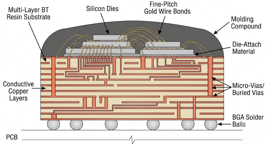
IC Packaging Substrates (BGA, CSP, and SiP)
Modern memory architectures like LPDDR5, UFS, and high-capacity NAND flash chips require extremely thin profiles with fine-pitch Ball Grid Array (BGA) configurations. BT resin serves as the rigid inner core for these multi-layer chip-scale packages (CSP) and System-in-Package (SiP) modules. Its structural stiffness ensures that during high-speed automated flip-chip or wire-bonding assembly, the carrier board resists bending or flexing under high mechanical and thermal pressure.
High-Frequency Communication Modules
In 5G base stations, satellite communication transceivers, and 400G/800G optical transceivers, high-frequency signal paths require pristine structural mediums. The low Dk and Df values of BT resin prevent signal attenuation, reduce parasitic capacitance, and preserve clean signal transitions. This capability allows RF front-end modules and power amplifiers to maintain optimal thermal management alongside minimal power dissipation.
Automotive Electronics Under Harsh Environments
Automotive under-the-hood control units, engine management sensors, and advanced driver-assistance systems (ADAS) millimeter-wave radar units face continuous, intense thermal cycling. Substrates based on BT resin excel here due to their exceptional thermal decomposition profile (Td of 350°C or higher) and robust resistance to electrochemical migration. This ensures that safety-critical automotive systems operate reliably over extended lifespans without localized electrical shorts or mechanical delamination.
Manufacturing Challenges of BT Resin PCBs
While BT resin offers excellent physical and electrical performance, it presents substantial manufacturing difficulties. Its strength, thermal resilience, and brittle nature require highly specialized processing equipment, even for rigid through-hole multi-layer configurations.
Mechanical Drilling Challenges & Solutions
- Mechanical Drilling Hurdles: Because of its dense polymer cross-linking, BT resin is significantly harder and more brittle than standard epoxy-glass (FR4) substrates. Standard drilling bits wear out rapidly or can cause internal micro-fracturing along the hole walls if the feed rate is not perfectly calibrated.
- The Risk of Smear: High-speed mechanical drilling creates immense localized friction and heat, which can generate resilient resin smear across internal copper foil layers, risking open circuits.
- The Solution: Fabricators must utilize ultra-sharp, diamond-coated solid carbide drills combined with optimized spindle speeds and precise chemical desmear operations to guarantee completely pristine, reliable plated through-hole (PTH) interconnects.
Laser Drilling and Microvia Formation
Laser Drilling Challenges & Solutions
- The Danger of Fracturing: Incorrect laser tuning can cause micro-fracturing along the via wall.
- The Risk of Smear: Excessive localized heating can generate resilient resin smear across internal copper interfaces.
- The Solution: Fabricators must use advanced UV/CO2 hybrid laser drilling systems combined with precise plasma chemical desmear operations to guarantee pristine structural integrity for subsequent copper plating.
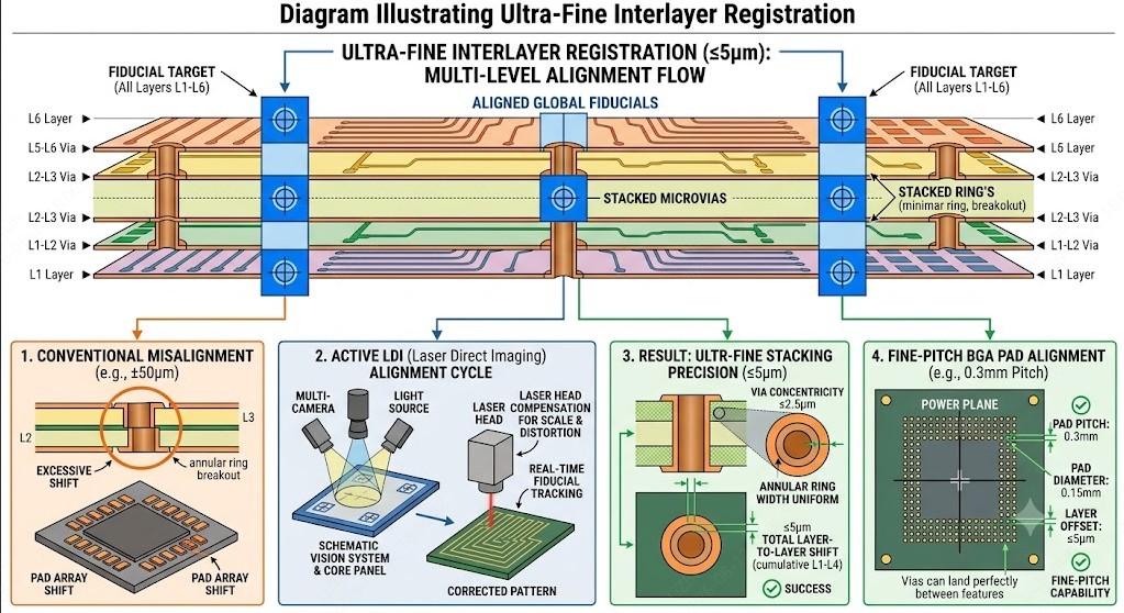
Layer-to-Layer Registration in Multilayer Substrates
With trace configurations moving toward ultra-fine lines and spaces (under 25 microns for high-density IC applications), even minimal dimensional shifts during lamination can cause interlayer misalignments.
BT resin undergoes highly predictable yet significant chemical shrinkage during its high-temperature curing process. Fabricators must use advanced predictive scaling models to compensate for material shifting beforehand, paired with pinless induction lamination systems, to guarantee perfect layer-to-layer registration across multi-layer high-density interconnect (HDI) constructions.
Surface Finish Compatibility for Semiconductor Bonding
An IC substrate must provide an exceptionally flat, coplanar surface for wire bonding or flip-chip solder bumps. Standard Hot Air Solder Leveling (HASL) is entirely unsuited for these tight tolerances.
The substrate requires premium Electroless Nickel Immersion Gold (ENIG) or Electroless Nickel Electroless Palladium Immersion Gold (ENEPIG) surface finishes. Depositing these ultra-thin metallic layers requires precise chemical control systems to prevent hyper-corrosion (often called "black pad") along the nickel interface, which can jeopardize the strength of gold or copper wire bonds.
How JLCPCB Delivers Excellence in BT Resin and High-Reliability PCB Fabrication
Addressing the manufacturing challenges of BT resin requires an ecosystem built on automated high-precision equipment, strict quality assurance protocols, and streamlined production workflows. As a world-class electronics manufacturing partner, JLCPCB has systematically optimized its production lines to process advanced materials with exceptional precision.
State-of-the-Art Production Facilities and Equipment
JLCPCB has deployed major infrastructure investments across its automated smart factories to handle high-tier, low-loss, and high-frequency materials. To achieve the precise alignments required by BT resin designs, JLCPCB uses state-of-the-art Laser Direct Imaging (LDI) systems, replacing traditional film masking. This technology enables ultra-precise trace resolution with tight line/space tolerances.
Furthermore, our automated UV/CO2 hybrid laser drills effortlessly create clean microvias through tough BT resin matrices without causing internal fractures, ensuring robust interconnect pathways for advanced multi-layer stackups.
Equipment Integration Efficiency
- Advanced LDI System: Ensures perfect fine-line trace realization down to precision tolerances.
- Hybrid Laser Drills: Creates clean, smear-free microvias under 75 microns.
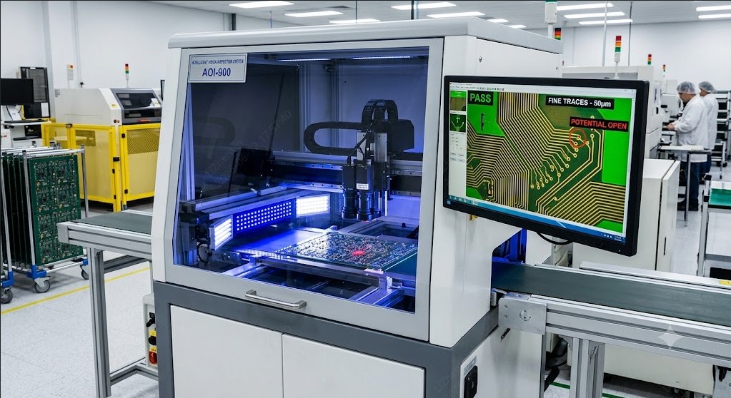
- Automated Line Scan: Real-time defect isolation via in-line automated optical inspection.
Stringent Quality Control and Material Sourcing
Quality at JLCPCB begins with premium, authenticated material sourcing. By partnering exclusively with industry-leading global laminate suppliers, JLCPCB ensures that every batch of BT resin processed meets rigorous Grade-A quality standards with completely uniform Tg, Dk, and Df baselines.
Our quality control framework incorporates several advanced verification steps:
- In-line Automated Optical Inspection (AOI) to scan every layer for trace defects.
- Automated X-ray Inspection (AXI) to analyze internal layer registration with sub-micron accuracy.
- Extensive reliability testing including Thermal Shock Profiling, Interconnect Stress Testing (IST), and Conductive Anodic Filament (CAF) resistance evaluation to validate compliance with IPC Class 2 and Class 3 industrial safety standards.
Seamless Transition from Prototype to Mass Production
Historically, obtaining prototype runs of high-tier BT resin or IC-grade substrates meant dealing with high minimum order quantities (MOQs) and lengthy lead times from traditional specialty fabricators. JLCPCB has transformed this dynamic by introducing an agile, digitalized smart manufacturing architecture.
Engineers, hardware innovators, and enterprise R&D groups can easily upload their high-density designs, configure advanced material stackups, and launch prototype runs with short turnaround times. Once the initial prototype is validated, JLCPCB's highly scalable manufacturing ecosystem seamlessly transitions the project to volume mass production, ensuring consistent yield rates, optimized cost-efficiency, and predictable lead times.
FAQ about BT Resin Packaging
Q: What is BT resin and how does it differ from standard FR4?
BT resin (Bismaleimide-Triazine) is a high-performance thermoset polymer co-polymerized from bismaleimide and triazine cyanate ester. Compared to standard FR4, it offers significantly higher glass transition temperature (180°C–210°C vs. 130°C–140°C), lower CTE (25–30 vs. 50–60 ppm/°C), lower dielectric constant and dissipation factor, and dramatically lower moisture absorption (under 0.05% vs. 0.15%–0.25%). These properties make BT resin essential for high-frequency, high-reliability IC packaging applications.
Q: What are the primary applications of BT resin PCBs?
BT resin PCBs are primarily used in IC packaging substrates including BGA, CSP, and SiP modules for advanced memory architectures (LPDDR5, UFS, NAND flash). They are also critical in high-frequency communication modules such as 5G base stations, satellite transceivers, and 400G/800G optical transceivers, as well as automotive electronics including ADAS millimeter-wave radar and engine management systems that face intense thermal cycling.
Q: Why is BT resin more challenging to manufacture than FR4?
BT resin's dense polymer cross-linking makes it significantly harder and more brittle than FR4, causing accelerated drill bit wear and potential micro-fracturing. High-speed drilling generates localized heat that can create resin smear across copper layers. Manufacturing requires specialized diamond-coated solid carbide drills, UV/CO2 hybrid laser systems, precise chemical/plasma desmear processes, and advanced predictive scaling models for layer-to-layer registration.
Q: What surface finish should be used for BT resin IC substrates?
Standard HASL is entirely unsuitable for BT resin IC substrates due to the stringent flatness and coplanarity requirements for wire bonding and flip-chip bumps. Instead, premium ENIG (Electroless Nickel Immersion Gold) or ENEPIG (Electroless Nickel Electroless Palladium Immersion Gold) finishes must be used, deposited with precise chemical control to prevent "black pad" hyper-corrosion at the nickel interface.
Q: Can JLCPCB support BT resin PCB projects from prototype to mass production?
Yes. JLCPCB's agile, digitalized smart manufacturing architecture supports the full lifecycle — from initial prototype runs with short turnaround times to seamless scaling into volume mass production. The platform features automated LDI systems, UV/CO2 hybrid laser drilling, in-line AOI/AXI inspection, and IPC Class 2/3 reliability validation to ensure consistent quality and cost-efficiency at every stage.
Conclusion: Accelerate Your BT Resin Designs with JLCPCB
As modern hardware demands extreme miniaturization and robust high-frequency paths, material selection directly dictates market success. With its exceptional thermal endurance, ultra-low dielectric loss, and structural resilience against electromigration, BT resin has become irreplaceable for next-generation advanced IC packaging, high-tier telecom modules, and automotive radar systems.
However, realizing the full potential of this brittle, ultra-hard polymer requires a manufacturing partner with elite processing precision. JLCPCB bridges the gap between advanced material science and accessible, high-yield fabrication. By combining automated LDI tracking, specialized hybrid laser micro-drilling, and rigorous IPC Class 3 quality validation, we eliminate traditional high-cost and long-lead barriers for high-tier substrates.
Keep Learning
Choosing the Right CTI Value for Safer High-Voltage PCBs
Key Takeaways Higher CTI (≥600V, Group I) allows shorter creepage distances while preventing surface tracking in high-voltage designs. Standard FR4 (CTI ~175V) is often inadequate for mains voltage — upgrade to high-CTI materials for safety and compactness. Always match CTI material group to your working voltage and pollution degree for IEC/UL compliance. Clean assembly and good layout practices are essential to realize the full benefits of high-CTI laminates. Choose certified high-CTI materials and e......
Why Choosing the Right TG Value Leads to More Reliable PCBs
Key Takeaways Tg is key to PCB reliability — it determines when the material loses rigidity under heat. Choose high Tg (≥170°C) for automotive, industrial, or multilayer boards to reduce expansion stress and delamination. Standard Tg (130–140°C) is sufficient for low-power consumer electronics. Higher Tg delivers better thermal stability, especially during lead-free soldering and thermal cycling. Right Tg choice = fewer failures and lower long-term costs. Did you ever question how it's possible for 2 ......
Choosing the PCB Laminate for Reliable High-Performance Boards
Key Takeaways Choosing the right PCB laminate is the foundation of a reliable high-performance board. Match your material to the application — standard FR4 for basic designs under 5 GHz, high-Tg FR4 for lead-free assembly, low-loss materials for high-speed digital, and Rogers/PTFE for RF and mmWave applications. Always prioritize stable Dk, low Df, high Tg, and low Z-axis CTE while recalculating your stackup for accurate impedance control. Partnering with an experienced manufacturer ensures optimal pr......
Mastering BT Resin Packaging: Technical Insights & JLCPCB Capabilities
Key Takeaways BT resin is a high-performance thermoset polymer with Tg of 180°C–210°C, ultra-low Dk/Df, and under 0.05% moisture absorption — essential for advanced IC packaging substrates (BGA, CSP, SiP). Its dense cross-linked structure provides superior resistance to electromigration, dendrite growth, and chemical degradation, making it ideal for fine-pitch, high-reliability applications. Manufacturing BT resin PCBs requires specialized diamond-coated drilling, UV/CO2 hybrid laser systems, and prec......
Selecting the Ideal Substrate Material for High-Performance PCBs
Key Takeaways Selecting the ideal PCB substrate material—balancing standard FR4 for general use with advanced Rogers or PTFE for high frequencies—is vital to prevent signal loss and thermal failure. Hybrid stackups perfectly optimize performance and cost , while JLCPCB guarantees a reliable, high-quality transition from rapid prototyping to volume production. Ever wonder what's under all those shiny copper traces on a printed circuit board? That layer is the substrate material, and it is probably the ......
PDN Design : Building Stable Power Delivery for High-Performance PCBs
Ever had to boot up a newly-built PCB only to discover that your FPGA won't boot up, your ADC inputs are not as clean as they should be, or your high-speed serial link is producing errors you did not get in simulation? Do not doubt your signal integrity work; just first review your PDN design. In many products that have failed to come to fruition, the problem is not the signal path but the power delivery to the signal path. A successful PCB is built upon a well-designed power distribution network, an ......