FPC Thickness Guide: How to Choose Flexible PCB Thickness
16 min
- What Is FPC Thickness?
- Standard FPC Thickness Range and Specifications
- How FPC Stackup Determines Overall Thickness
- How to Choose the Right FPC Thickness?
- Factors That Affect FPC Thickness Selection
- Thin FPC vs Thick FPC: Which One Should You Choose?
- JLCPCB's FPC Manufacturing Capabilities for Different Thickness Requirements
- Conclusion
- Frequently Asked Questions (FAQ)
Flexible PCB can bend, but how much? And here is why thickness becomes a crucial factor in flex PCB design. If we made the mistake, it would either become too thin and jiggle around inside a ZIF connector, or too thick, fatigue the outer copper and crack traces within a few thousand bend cycles. It is also the number most designers quietly leave to the fab. But today in this guide, we will cover:
- What an FPC thickness includes
- The range you can go up to and order
- How the stackup adds thickness layer by layer
- How to match thickness to bend radius, current, and connector fit
What Is FPC Thickness?
Definition of FPC Thickness
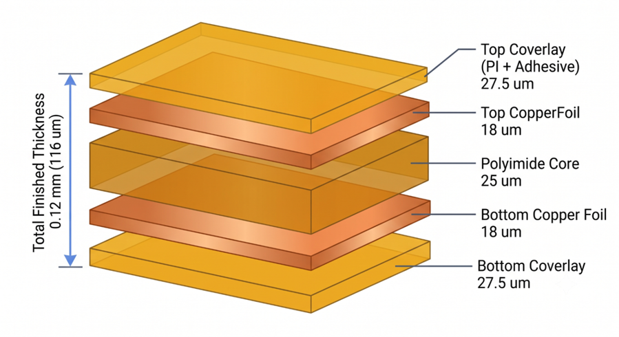
FPC thickness is the finished height of the flexible printed circuit measured through the entire stack-up (top coverlay, top copper, polyimide core, bottom copper, and bottom coverlay). It is measured in millimeters or microns, and usually does not include stiffeners unless a connector or component needs extra support.
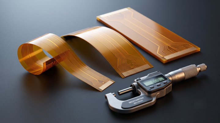
A quoted 0.12 mm two-layer flex describes only the bendable region; a stiffener bonded under the connector tail gives that area its own thickness and tolerance.
Note: Flex uses no liquid solder mask. Its protective layer is a laminated coverlay of polyimide and adhesive, which, at a thin build, accounts for over half of the total stack.
Why FPC Thickness Matters in Flexible Circuit Design
Fold one sheet of paper, and it creases without complaint. Fold ten around the same radius, and the outer sheets tear while the inner ones buckle. Thickness decides how many sheets your flex is being asked to fold.
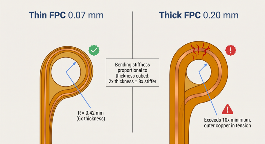
Stiffness is proportional to thickness cubed, so a change in thickness from 0.11 mm to 0.22 mm will increase the stiffness by a factor of 8, not 2. The stress on each trace at the crest of the fold is a linear function of strain in the outer copper scales: doubles the strain, doubles the stress.
A prototype fitness band lost its optical heart-rate sensor after three weeks of wear. The 0.20 mm flex was bent around a 0.6 mm radius, which is a 3x bend ratio when a 10x minimum bend ratio is required for two layers. The hairline fractures were identified by cross-sectioning in the outer 35 µm copper material at the fold crest, then cleared by rebuilding on a 0.11 mm stack with 18 µm copper.
Standard FPC Thickness Range and Specifications
Common Flexible PCB Thickness Options
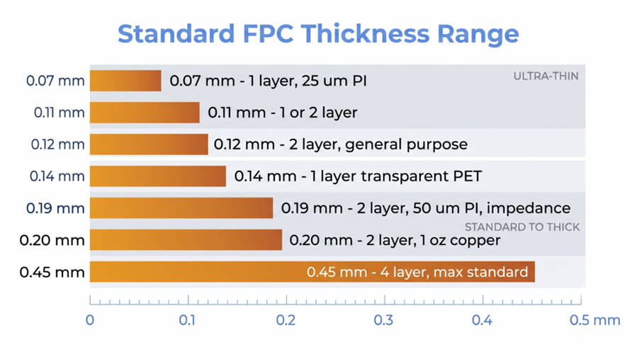
The range of flexible circuits is from 0.05 mm to 1.5 mm and includes heavy multilayer and rigid-flex constructions. For standard one, two, and four-layer FPCs, the working range is 0.07 to 0.45 mm.
| Finished Thickness | Layers | Core Dielectric | Best Suited For |
| 0.07 mm | 1 | 25 µm PI | Tightest dynamic bends, wearables |
| 0.11 mm | 1 or 2 | 25 µm PI | Space-constrained signal routing |
| 0.12 mm | 1 or 2 | 25 or 50 µm PI | General-purpose two-layer flex |
| 0.19 mm | 2 | 50 µm PI | Controlled impedance |
| 0.20 mm | 2 | 25 µm PI | 1 oz copper, higher current |
| 0.14 / 0.24 mm | 1 / 2 | Transparent PET | Backlit panels, light paths |
| 0.20 to 0.45 mm | 4 | 25 µm PI cores | Dense routing with planes |
Ultra-Thin FPC vs Standard FPC Thickness
Ultra-thin FPC means 0.10 mm or below, in practice, a single-layer build on a 25 µm polyimide core. At 0.07 mm, it is thinner than printer paper and conforms to almost any shape you fold it into.
But ultra-thin FPCs come with three critical compromises:
- Current capacity (these builds are only paired with 18 µm copper at most);
- Handling yield (for example, the panel is delicate through etch and test); and
- Impedance control (no second layer to reference).
Standard FPC thicknesses of 0.11 to 0.20 mm are where most designs land, with two copper layers for crossover routing and a ground plane. This is the space where the camera ribbon on a smartphone and the display cable on a laptop lid hinge reside.
How FPC Stackup Determines Overall Thickness
Key Layers That Affect FPC Thickness
The FPC stack-up is an arithmetic problem: each layer of the FPC has a known thickness in microns; the final thickness is the sum of the layer thicknesses:
- Coverlay (on each face): 27.5 - 50 µm of polyimide film and adhesive.
- Copper foil, each face: 12, 18, or 35 µm, set by current demand. The bottom foil mirrors the top, so the stack does not curl.
- Polyimide core: 25 or 50 µm, depending upon the impedance target.
- Stiffener, local and optional: 0.1 to 1.6 mm.
What most designers don't think of is the coverlay pairing. For copper 0.33 oz or 0.5 oz, 12.5 µm of polyimide plus 15 µm of adhesive will suffice. The next step is 1 oz, with the adhesive flowing around the taller traces; coverlay is now 25 µm polyimide plus 25 µm adhesive, a total of 50 µm per side. This is 45 µm before any additional copper is added.
How Layer Count Impacts FPC Thickness
Adding copper layers does not scale thickness linearly because each pair adds its own core and bonding adhesive, with no reduction elsewhere.
Example: A 0.12 mm two-layer flex is 27.5 + 18 + 25 + 18 + 27.5 = 116 µm. Switch to 1 oz copper with the heavier coverlay it demands, and the same stack reads 195 µm, the 0.20 mm option. It is built on a 50 µm core with 18 µm copper, and it comes to 186 µm, the 0.19 mm impedance option. Plating adds copper to the outer layers of a two-layer build, which is why fabs quote a nominal finished thickness.
FPC Stackup Examples for Different Applications
Three builds, each driven by a different constraint:
- Dynamic hinge cable, printer head or laptop lid: One layer, 25 µm PI, 18 µm rolled annealed copper. Finished at 0.07 mm, allowing a bend radius under 0.5 mm and millions of cycles.
- Two-layer sensor interconnects with a ground plane: 25 µm core, 18 µm copper, and 27.5 µm coverlay on both sides. Finished at 0.12 mm with crossover routing and a continuous return path.
- Four-layer flex for a dense module: Two 25 µm cores joined by a bonding layer, 12 µm copper throughout. Finished at 0.20 to 0.25 mm, signals referenced to internal planes.
How to Choose the Right FPC Thickness?
Consider Mechanical Flexibility Requirements
Start with the bend, because it sets a hard ceiling on everything else. Minimum bend radius is a multiple of the total finished thickness:
| Application | Minimum Bend Radius | Practical Note |
| Single-layer, static (bend to install) | 6x total thickness | 0.07 mm flex bends to a 0.42 mm radius |
| Double-layer, static | 10x total thickness | 0.12 mm flex needs a 1.2 mm radius |
| Multilayer, static | 15 to 20x total thickness | Keep four-layer flex out of fold zones |
| Dynamic flexing, continuous motion | 20 to 40x or more | High-cycle designs often need 100x |
A 1.0 mm housing radius with a double-layer static bend at 10x caps you at 0.10 mm, which points straight at the 0.07 mm build. Rolled annealed (RA) copper has elongated horizontal grains that survive repeated folding; electrodeposited (ED) copper has columnar grains that seed cracks.
Balance Thickness and Mechanical Strength
The flex circuit must also withstand pick-and-place, reflow, connector attachment, and the technician's fingers. An unsupported flex will not remain flat on a stencil nor hold components during reflow below approximately 0.10 mm. It is like a thin, rigid board with a thickness of 0.30 mm or more.
The answer is usually not a uniform thickness, but a thin flexible body, with local stiffening where strength is required:
- Under the connector tails, to reach the thickness the connector expects.
- Under component clusters, so reflow does not warp the assembly.
- At mounting holes, so the screw torque does not tear the polyimide.
- At the transition into a bend zone, it is necessary to control where flexing begins.
Consider Electrical Performance Requirements
Thickness drives impedance more strongly on flex than on rigid boards because the dielectric is measured in microns rather than mils. The dielectric constant of polyimide is approximately 3.3. A 50 Ω single-ended microstrip with a 25 µm core requires a trace width of approximately 1.9 mil. This is below the practical minimum of 3 mils; at the actual process limit of 2 mils, the ±20% width window causes the impedance to fall outside any useful operating range.
Moving to the 50 µm core and the same 50 Ω target requires about 96 µm, which is comfortably manufacturable. That is why the 0.19 mm build on 50 µm polyimide exists as a distinct option. When routing, if your flex has USB, MIPI, or LVDS, opt for the 50 µm dielectric first. The same discipline that applies to rigid PCB design rules applies here, but with much narrower margins.
Factors That Affect FPC Thickness Selection
Material Selection
With a headroom of 245-260 °C per IPC-4204 for lead-free reflow, polyimide is the default base material because it is ductile and dimensionally stable.
Thickness is directly controlled by 3 material decisions:
- Core thickness: The 25 µm core provides flexibility; the 50 µm core provides impedance control and robust handling.
- Adhesive vs adhesiveless laminate: Removes an acrylic layer of 12-25 µm from the polyimide and bonds copper without adhesive, providing higher thermal stability at a higher cost.
- Polyimide vs transparent PET: Transparent is built at 0.14 mm single layer, or 0.24 mm double layer (thicker than PI), since PET requires the heavier 25 µm coverlay pairing.
The poorest coefficient of thermal expansion in the stack is that of the acrylic adhesive, which means that the thickness of this adhesive will vary with temperature, and so will the impedance.
Copper Thickness and Current Carrying Requirements
The one factor you have control over, based on your electrical requirements, is copper weight. The options are 12 µm, 18 µm, and 35 µm , with single-layer builds starting at 18 µm. Current capacity is directly proportional to cross-sectional area; if the copper weight is halved, the trace width must be doubled to maintain the same capacity at the same current. A 1.0 mm trace in 35 µm copper will carry 2 to 3 A with an increase of 20 °C in the exposed outer layer, while a 1.0 mm trace in 12 µm copper will carry about 1 A.
Verify those numbers with IPC-2152. A flex cooling in still air inside a plastic enclosure is far worse than the open test coupons the charts were made from, and there are no copper planes to spread the heat. Copper weight cuts both ways. Going to 1 oz adds 34 µm across a two-layer stack directly, then forces the thicker coverlay for another 45 µm. Your 0.12 mm flex becomes a 0.20 mm flex, and its minimum bend radius grows from 1.2 mm to 2.0 mm.
Stiffener Requirements
Stiffeners are the areas where FPC thickness is a mechanical fit and a specific thickness is targeted. The 0.5 mm pitch ZIF connectors require a certain thickness for insertion. Put that tail in direct, and the contacts never get enough normal force: the joint reads fine on the bench and falls off under vibration; it is the Hirose FH12 series that specifies 0.30mm ± 0.05mm; you have a bare two-layer flex that is 0.11mm to 0.20mm.
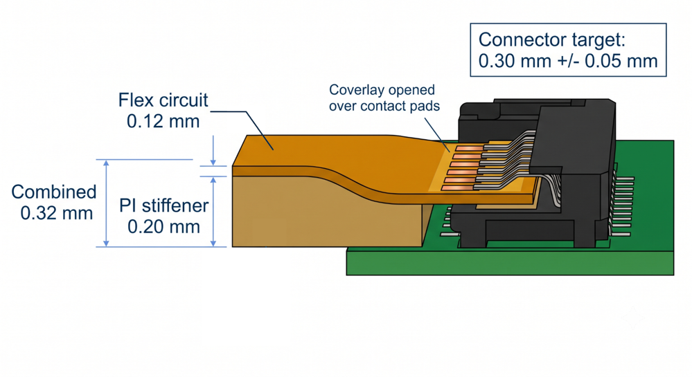
To correct this, glue a stiffener on the other side of the tail so that the pair of thicknesses falls within the connector's window, minus flex. A 0.12mm flex and a 0.2mm PI stiffener will provide 0.32mm, and a 0.2mm flex and a 0.1mm PI stiffener will provide exactly 0.30mm, both within the ±0.05mm window. The polyimide stiffeners are 0.1 to 0.25 mm thick for connector tails; FR4 is 0.1 to 1.6 mm thick for component mounting and screw-down points, and stainless steel is 0.1 to 0.3 mm thick for the highest stiffness in the lowest height.
Thin FPC vs Thick FPC: Which One Should You Choose?
Advantages of Thin Flexible PCB
Thin builds at 0.07 to 0.12 mm win wherever motion or volume is the binding constraint:
- Much smaller bend radius – 0.07 mm static vs 0.42 mm.
- Stiffness that is much less as a function of thickness cubed.
- Extended fatigue life – millions of fatigue cycles versus thousands.
- Reduced mass and volume – applicable to wearables and hearing aids.
- True conformability in 3-D around curved housings and back on itself.
Advantages of Thick Flexible PCB
Thicker builds at 0.19 to 0.45 mm win wherever the circuit has a job beyond bending:
- Thicker gauges, as thickness generally comes with 1 oz copper.
- Practical controlled impedance – a 50 µm dielectric allows manufacturable widths at 50 Ω.
- Improved component support via reflow, reduced warping, and tombstone.
- Additional routing layers for high-density designs with suitable reference planes.
- Better handling and assembly in a volume production.
Thin vs Thick FPC Comparison
Thin flex is 12 to 18 µm copper, has a thin – 0.4 to 1.2 mm static radius, and requires a stiffener before it can support components. Thick flex with 18-35µ copper, 2-4 layers, and a 1.9-9.0mm radius, and an impedance that can be repeated. Use this mapping to convert a requirement into a build:
| If Your Design Needs | Choose This Thickness | Typical Build |
| Dynamic bending, high cycle count | 0.07 mm | 1-layer, 25 µm PI, 18 µm RA copper |
| A tight one-time fold in a wearable | 0.11 mm | 2-layer, 25 µm PI, 12 µm copper |
| Controlled 50 Ω single-ended routing | 0.19 mm | 2-layer, 50 µm PI, 18 µm copper |
| 2 A or more of current | 0.20 mm | 2-layer, 25 µm PI, 35 µm copper |
| Reference planes plus dense routing | 0.25 to 0.45 mm | 4-layer with a bonding layer |
| Direct ZIF connector insertion | 0.30 mm at the tail | Any build plus a PI stiffener |
JLCPCB's FPC Manufacturing Capabilities for Different Thickness Requirements
Flexible PCB Thickness Options and Customization
All the thicknesses featured in this guide are from actual production menus. JLCPCB fabricates 1-layer, 2-layer, and 4-layer flex with thicknesses of 0.07 mm–0.45 mm on 25 µm or 50 µm polyimide and transparent PET at 0.14 mm or 0.24 mm.

The key is the combinations below: copper thickness from 12µm to 18µm to 35µm; coverlay in yellow, black, white, or transparent; adhesive or adhesiveless laminate; and stiffeners from PI to FR4, stainless steel to 3M films, all the way from 0.05 to 1.6 mm. That width allows you to solve the connector fit and bend radius problems independently, in a single build.
Advanced Manufacturing Process Ensuring Thickness Accuracy
If the finished part does not meet the thickness specification, it is of no use. The big deal is vacuum lamination: bonding thin polyimide films and coverlays without trapped air or misregistration keeps the stack straight throughout an entire panel.
Stiffeners up to 0.3 mm are held to ±0.05 mm, 0.3 to 1.0 mm to ±0.1 mm, and above 1.0 mm to ±10%. Trace width has a tolerance of ±20%, which sets the impedance repeatability, while the outline has a tolerance of ±0.1 mm, reduced to ±0.05 mm upon request. The gold finger area is even tighter, ±0.03 mm. This is the number to use to verify a connector target of 0.30 mm, which is where the thickness becomes an electrical contact.
Reliable FPC Manufacturing for Various Applications
Flex doesn't tolerate even the smallest mistakes. A via within a bend zone, a trace parallel to a fold line, or a stiffener that doesn't reach the connector opening passes schematic and then fails in hardware. Automated DFM review identifies bend-zone hazards, spacing violations, and stackups early enough in the CAD design to be corrected, and then manages the prototype through volume. Once you have a validated stackup ready for hardware, request a flex PCB quote and observe the flex PCB thickness, copper weight, stiffener options, and how they affect pricing and lead time.
Conclusion
FPC thickness is not a single number you pick at the end of a design. It is the output of four constraints that pull against each other: the bend radius your housing allows, the current your traces carry, the impedance your signals demand, and the thickness your connector expects. Work each to a number, then find the build that satisfies all four.
The habit worth keeping is arithmetic. Every layer contributes a known thickness, so you can compute a stack before you order it and check it against a 6x or 10x bend ratio. On rigid boards, thickness selection is mostly mechanical; on flex, it is mechanical, electrical, and thermal at once.

Frequently Asked Questions (FAQ)
What Is the Standard Thickness of an FPC?
Ans: Standard FPC thickness runs from about 0.07 mm to 0.45 mm, with 0.11 mm to 0.20 mm covering most two-layer designs. Four-layer builds begin at 0.20 mm. These figures describe the flexible region only and exclude any local stiffener.
What Factors Determine FPC Thickness?
Ans: Five layers make up the total: a coverlay on each face, copper foil on each face, and the polyimide core between them. You choose copper weight and core dielectric directly; coverlay thickness then follows from the copper weight. Stiffeners add thickness locally and are quoted separately.
How Do I Choose the Right FPC Thickness?
Ans: Work backward from your tightest constraint. Divide the bend radius your housing allows by the applicable ratio, 6x for single-layer static, 10x for double-layer, 20x or more for dynamic, to get a maximum thickness. Check that it still supports your current and impedance needs, then size any stiffener as the connector's target minus your finished flex.
Does Copper Thickness Affect FPC Thickness?
Ans: Yes, and by more than the copper itself. Moving from 18 µm to 35 µm copper adds 34 µm directly, then requires a thicker coverlay pairing, adding another 45 µm. A 0.12 mm flex becomes a 0.20 mm flex, and its bend radius nearly doubles.
What Is the Thinnest Flexible PCB Available?
Ans: The thinnest standard production build is 0.07 mm: a single-layer circuit on a 25 µm polyimide core with 18 µm copper and a thin coverlay. It folds to a static radius of roughly 0.42 mm. Specialty processes go below this, but 0.07 mm is the practical floor.

Popular Articles
• Choosing the Right Bend Radius for Durable Flexible PCBs
• Flexible Meets Durable: Understanding Rigid-Flex PCB Technology
• PCB Stiffeners: An Essential Requirement for Flexible Circuits
• The Ultimate Guide to Flexible PCB: Types, Design, and Applications
• 45 Must-Know Flex PCB Design Tips You Can't Afford to Miss!
Keep Learning
Choosing the Right Bend Radius for Durable Flexible PCBs
Key Takeaways Mastering the bend radius is essential for reliable flexible PCB design. Following IPC-2223 guidelines, maintain a minimum of 6× total thickness for static bends and 100× for dynamic applications, while using thinner RA copper, adhesiveless polyimide, staggered traces, and cross-hatched patterns in flex zones. Proper material selection, layer stackup optimization, and adequate clearance from stiffeners can dramatically extend flex life and prevent premature trace cracking or delamination......
Flex PCB Stackup Design Guide: Layers, Materials & Reliability
Key Takeaways A reliable flex PCB starts with the right stackup design. The layer structure, material selection, and copper arrangement directly affect flexibility, bend life, electrical performance, and manufacturing reliability. This guide explains single-sided, double-sided, and multilayer flex PCB stackups, including polyimide materials, coverlay, copper types, and key design considerations for creating durable flexible circuits with JLCPCB. Did you ever wonder how a foldable phone can last for 20......
Flexible Meets Durable: Understanding Rigid-Flex PCB Technology
In the rapidly evolving world of electronics, the demand for smaller, more reliable, and more versatile devices continues to grow. To meet these demands, engineers and designers are increasingly turning to Rigid-Flex PCBs. The circuit boards combine rigid and flexible substrates into a single interconnected structure. This combination allows for complex designs that can bend and flex in specific areas while maintaining rigidity in others. To manufacture rigid flex PCBs, IPC offers advice and best prac......
PCB Stiffeners: An Essential Requirement for Flexible Circuits
A printed circuit board stiffener plays an important role when it comes to offering mechanical support to a PCB. They are particularly helpful for flexible circuit boards, that given their name, are flexible and in need of stiffness in certain places. Stiffeners are particularly required when components are placed in a flex zone & the weight of these components stresses the flex material. These components provide a rigid connection from the flexible portion to the solid board. This solidity makes appl......
The Ultimate Guide to Flexible PCB: Types, Design, and Applications
Key Takeaways JLCPCB 1–4 Layer Flex PCB: Supports 1 to 4-layer FPCs with polyimide (PI) substrates and trace/space down to 3/3 mil. Stiffener Selection: Use PI (0.1–0.25mm) for ZIF connectors, FR4 (0.1–1.6mm) for SMT support, and Stainless Steel (0.1–0.3mm) for high rigidity. Layout Optimization: Use cross-hatched copper ground planes and stagger 2-layer traces to eliminate the "I-Beam effect." Surface & Protection: Combine Immersion Gold (ENIG 1u"/2u") for SMT planarity with flex coverlay to protect ......
Medical Flex Circuits: Manufacturing, Applications, Materials, and Design Guide
Medical flex circuits made to fit inside a 1.0 mm disposable endoscope, wrap around a hearing aid shell, and sit on a patient's arm for ten straight days. When one fails, it is not a warranty return but a device history file and a regulatory conversation. In this guide, you will learn: What separates a medical flex circuit from a consumer one How they are built, tested, and released Polyimide, copper, coverlay, and stiffener choices Fine line, bend radius, and layer count limits What to check before c......