
Everything You Need to Know about BGA Technology in PCB Assembly
10 min
- What is Ball Grid Array (BGA)?
- Types of BGA (Ball Grid Array) Packages
- Advantages and Disadvantages of Ball Grid Array (BGA)
- Typical Applications of BGA Technology
- BGA Applications in PCB Assembly
- BGA Inspection Techniques
- Common BGA Defects and How to Fix Them
- FAQ about BGA (Ball Grid Array)
Ball Grid Array (BGA) is a leadless surface-mount package widely used in high-density and high-speed PCB designs.
It features an array of solder balls on the underside, providing high I/O density, better signal integrity, and thermal performance.
This guide covers what is BGA, different types of BGA packages, advantages and disadvantages, assembly requirements, inspection methods, and common defect solutions, helping engineers make informed decisions in PCB manufacturing.
What is Ball Grid Array (BGA)?
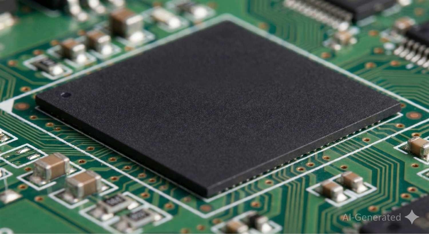
A Ball Grid Array (BGA) is a leadless surface-mount device (SMD) package in which electrical connections are made through an array of solder balls located on the bottom of the package.
Inside the BGA package, a laminated substrate routes electrical signals from the silicon die to the solder balls using fine metal traces. During PCB assembly, these solder balls are reflowed to corresponding pads on the PCB, forming both electrical and mechanical connections.
Compared with traditional leaded packages such as QFP and DIP, BGA packages provide significantly higher I/O density, shorter interconnect lengths, and superior performance in high-speed and high-frequency applications.
Types of BGA (Ball Grid Array) Packages
Ball Grid Array (BGA) packages come in several variants, each designed to meet different electrical, thermal, and mechanical requirements. Below are some of the most common BGA package types used in modern PCB assembly.
1. PBGA (Plastic Ball Grid Array): PBGA uses an organic substrate, typically FR-4 or BT resin, with an epoxy-molded plastic body. It offers a good balance of cost, performance, and manufacturability, making it widely used in consumer electronics and general-purpose ICs.
2. FCBGA (Flip-Chip Ball Grid Array): In a Flip-Chip BGA, the silicon die is mounted face-down onto the substrate using solder micro-bumps. This design shortens signal paths and improves electrical and thermal performance, making FCBGA ideal for high-performance processors, GPUs, and networking chips.
3. CBGA (Ceramic Ball Grid Array): CBGA uses a ceramic substrate, which provides excellent thermal stability and a close coefficient of thermal expansion (CTE) match with silicon. It is commonly used in high-reliability applications such as aerospace, military, and industrial systems.
4. CDPBGA (Cavity-Down Plastic Ball Grid Array): CDPBGA features a recessed cavity in the substrate where the die is mounted closer to the PCB. This structure improves heat dissipation and reduces overall package height compared to standard PBGA designs.
5. TBGA (Tape Ball Grid Array): TBGA uses a flexible polyimide tape substrate instead of a rigid PCB. While it offers low weight and good electrical performance, TBGA is less common today due to mechanical reliability and handling limitations.
6. H-PBGA (High-Thermal Plastic Ball Grid Array): H-PBGA enhances standard PBGA designs by incorporating improved thermal paths, such as a metal heat spreader. It is suitable for devices that require better heat dissipation without moving to ceramic packages.
Learn more: 7 Types of BGA (Ball Grid Array) Packages Explained
Package on Package (PoP)
Package on Package (PoP) is an advanced BGA stacking technology in which multiple BGA packages are vertically stacked and electrically interconnected.
PoP is commonly used to integrate memory devices on top of logic processors, allowing higher functional integration while maintaining a compact PCB footprint. This structure is widely adopted in smartphones, embedded systems, and high-performance computing devices.
Advantages and Disadvantages of Ball Grid Array (BGA)
Advantages of BGA Packages
Highest I/O Density: BGAs support hundreds or even thousands of connections within a compact footprint, far exceeding the pin density achievable with QFN and leaded packages.
Superior High-Speed Performance: Extremely short interconnections between the die and solder balls minimize parasitic inductance and resistance, making BGAs ideal for high-speed devices such as FPGAs, CPUs, and advanced microcontrollers.
Efficient Thermal Dissipation: The solder ball array and substrate structure provide multiple heat transfer paths, improving thermal performance in high-power applications.
High Mechanical and Electrical Reliability: Uniform stress distribution and robust solder joints enhance long-term reliability under thermal cycling and vibration.
Challenges and Limitations of BGA Packages
Complex Assembly Requirements: BGA assembly demands high placement accuracy, controlled reflow profiles, and stable process control to avoid defects such as head-in-pillow and voiding.
Difficult PCB Routing and Fabrication: Escaping signals from dense BGA arrays often requires multi-layer stack-ups, microvias, and via-in-pad (VIP) structures, increasing fabrication complexity and cost.
Limited Visual Inspection and Rework: All solder joints are hidden beneath the package, making optical inspection impossible. X-ray inspection is essential, and rework requires specialized equipment and skilled operators.
Strict Handling and Storage Conditions: BGAs are sensitive to moisture and ESD. Improper storage or baking control may lead to popcorning, delamination, and long-term reliability issues.
JLCPCB can handle complex BGA-based designs with advanced PCB manufacturing and assembly capabilities, including multi-layer PCBs and via-in-pad technology.
Typical Applications of BGA Technology
BGA packages are widely used in industries where space efficiency and signal integrity are key:
1. High-density motherboards: Laptops, servers, and gaming consoles rely on BGA-packaged processors, chipsets, and memory modules.
2. Telecommunication equipment: Routers, base stations, and network switches use BGA devices for high-speed signal processing.
3. Consumer electronics: Smartphones, tablets, and wearable devices benefit from BGAs’ compact size and improved thermal performance.
Typical Devices That Use BGA Packages
BGA Applications in PCB Assembly
Ball Grid Array (BGA) technology has become a cornerstone in modern PCB assembly, especially for products that demand high reliability and compact design. Compared to traditional leaded packages, BGAs enable more I/O connections within a smaller footprint, making them an essential choice in today's high-density electronic systems.
SMT Requirements for BGA Placement
To successfully assemble BGAs, manufacturers must follow strict Surface Mount Technology (SMT) requirements:
1. Stencil design and solder paste selection: The stencil aperture size and solder paste viscosity directly affect solder joint quality. A uniform solder paste deposit is critical to avoid bridging or voids.
2. Pick-and-place precision: BGA packages demand higher placement accuracy compared to other components. Misalignment can lead to hidden soldering defects.
3. Reflow profile control: A well-optimized reflow oven temperature curve ensures proper solder ball wetting without overheating, which could damage the package or PCB.
Key Considerations in BGA Assembly
Engineers must address several challenges during PCB design and assembly to ensure long-term reliability of BGA joints:
1. PCB layout density: Proper pad design and via placement are critical to accommodate escape routing of BGA balls.
2. Solder ball pitch: Finer pitches increase I/O density but also raise manufacturing complexity.
3. Thermal management: BGAs with high power consumption require thermal vias and adequate copper planes to dissipate heat effectively.
By understanding these application requirements and design considerations, engineers can fully leverage the benefits of BGA technology while minimizing assembly risks.
BGA Inspection Techniques
Note
Why AOI Is Not Enough for BGAs?
Automated Optical Inspection (AOI) uses cameras to check component presence. Since BGA joints are hidden, AOI can only inspect the outer row of balls, leaving 90% of the connections unverified.
Automated X-ray Inspection (AXI)
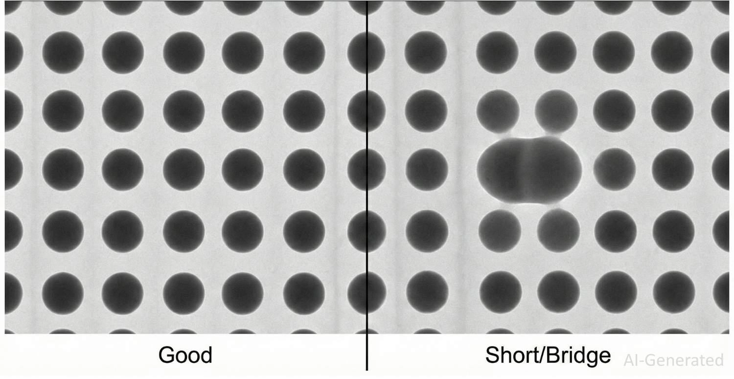
To guarantee assembly quality, JLCPCB performs X-ray inspection on all BGA assemblies. AXI uses X-rays to penetrate the package and generate grayscale images based on material density, allowing hidden solder joints to be analyzed.
This method is essential for detecting defects that cannot be identified through visual inspection.
Electrical Test and Boundary Scan
For functional verification, electrical testing methods such as JTAG boundary scan can be used to confirm proper connectivity of BGA pins. Boundary scan enables engineers to test interconnections electronically without physical probing. However, this method requires specific design considerations, such as dedicated test access points and compatible circuitry.
Common BGA Defects and How to Fix Them
Detaching of components: BGA component faults can be rectified by first detaching the components from the circuit board. It can be done by careful heating of localized components on board, which melts down the solder joints, and we can change the components and fix the solder connections as required.
BGA rework process: BGA rework process is done in a dedicated rework station in the factory., where BGA-PCB components are heated through an infrared heater. Heat level can be checked by thermocouple. To raise the package from the underlyingboard a vacuum device is used along with other equipment.
Localized heating: the heating process is done very carefully and it is limited to the defect area on the board. Localized heating ensures the safety of neighboring components on the board.
FAQ about BGA (Ball Grid Array)
Q: Is it cheaper to use Via-in-Pad on a 4-layer board or upgrade to 6 layers for BGA routing?
Surprisingly, it is often more cost-effective to upgrade to a 6-layer board at JLCPCB. Standard Via-in-Pad (VIP) on 4-layer boards is a premium, complex process. However, JLCPCB offers free POFV (Plated Over Filled Via) specifically on 6-layer and higher stack-ups. This means upgrading the layer count can actually lower your total production cost while simplifying your BGA escape routing.
Q: How should I terminate unused BGA I/O pins?
Unused input pins should never be left floating since they will likely pick up noise and act as antennas. The best way to handle them is to connect them to Ground or VCC, depending on the recommendations in the datasheet. Floating of unused output pins is a normal practice across the board. If we are talking about high-frequency BGAs, configuring unused pins as ground points could provide additional shielding while improving thermal dissipation.
Q: When is "Underfill" recommended for BGA packages?
Underfill, the resin used to fill the gap between the BGA and the PCB, is not a necessity for normal static devices (like routers). But on the contrary, it is highly recommended for mobile devices or car electronics that will undergo mechanical shocks, vibrations, or fall tests. The underfill acts as a stress redistributor and moves the stress away from the solder joints, thus avoiding fatigue cracking.
Q: Can I place decoupling capacitors directly under the BGA on the bottom layer?
Yes, placing capacitors directly underneath (on the bottom side) is excellent for minimizing loop inductance and ensuring power integrity. However, ensure you leave sufficient clearance for the pick-and-place nozzle support if the board undergoes double-sided assembly.
Q: My BGA components have been in loose storage. Will "popcorning" be an issue?
If your BGAs have been exposed to ambient humidity beyond their Moisture Sensitivity Level (MSL) rating, absorbed moisture will turn to steam during reflow, cracking the package (popcorning). If you are supplying parts, you must bake them according to J-STD-033 before assembly. For parts sourced via the JLCPCB Parts Library, strict climate-controlled storage is handled automatically.
Popular Articles
• SMD Diode Code Lookup: Full List, Marking Guide & Identification [2026 Guide]
• SMD Resistor Package Sizes: Complete Size Chart, Footprints & How to Choose
• SMD Capacitor Codes: Identification, Markings, and Polarity
• SMD Capacitor Sizes: Complete Size Chart and Selection Tips for PCB Design and Assembly
• How to Solder SMD Components Like a Pro [2026 Updated]
Keep Learning
PoP Package (Package on Package) Explained: Architecture, Assembly, and SMT Challenges
In the race for miniaturization, fitting more processing power into smaller footprints is the ultimate challenge for PCB designers. Package on Package (PoP) technology answers this by integrating logic and memory vertically, becoming the standard for modern mobile processors. However, this 3D architecture demands advanced SMT assembly capabilities beyond standard fabrication. JLCPCB specializes in the high-precision manufacturing required to master these complex stacks. This guide covers how PoP packa......
What Is a PQFP Package? Plastic Quad Flat Package Design, Footprint, and Assembly Guide
The Plastic Quad Flat Package (PQFP) is a widely used IC package in industrial, automotive, and embedded designs. This article provides a practical, engineering-focused guide to PQFP package. It explains how PQFP is built, when it makes sense to use it, how it compares with newer package types, and what designers should consider in terms of footprint design, thermal performance, signal integrity, manufacturing, and reliability. What Is a PQFP Package (Plastic Quad Flat Package)? A Plastic Quad Flat Pa......
Small Outline Integrated Circuit (SOIC): Package, Specs & Uses
As designs transition from legacy through-hole components to high-density Surface Mount Technology (SMT), the Small Outline Integrated Circuit (SOIC) remains the industry standard for operational amplifiers, flash memory, sensors, and microcontrollers. It stands as a testament to balanced engineering, offering a perfect compromise between the miniaturisation demanded by modern consumer electronics and the ruggedness required for industrial applications. This article serves as a definitive engineering ......
A Complete Guide to Surface Mount Device (SMD)
Imagine holding a smartphone in your hand. Inside that sleek device lies a complex network of thousands of miniature components — resistors smaller than a grain of rice, capacitors thinner than a fingernail, and integrated circuits containing millions of transistors. Without Surface Mount Technology (SMT) and its compact Surface Mount Devices (SMDs), none of this would exist. Just a few decades ago, electronics were bulky. Radios filled desks, computers filled rooms, and assembling a circuit meant dri......
Circuit Breaker Types Explained: MCB, MCCB, RCCB, RCBO, ACB, VCB & SF6 Circuit Breakers
A circuit breaker automatically disconnects power when it detects faults such as overloads or short circuits, protecting equipment and reducing fire risk. Different circuit breaker types are designed for different voltage levels, current ratings, and applications, from household distribution boards to high-voltage substations. This guide explains the most common types - including MCBs, MCCBs, RCCBs, RCBOs, ACBs, VCBs, and SF6 breakers and helps you choose the right one for your application. Figure: Ci......
Quad Flat Package (QFP): The Engineer's Guide to Design, Assembly and Thermal Management
What is QFP Package? The Quad Flat Package (QFP) is one of the most popular surface mount technology (SMT) package formats throughout the history of electronic manufacturing. After it became standard in the 1980s, the QFP has been the industry standard for integrated circuits (ICs) with moderate to high pin counts that typically range from 32 to 304 pins, so it was a good alternative for simple SOIC packages and complex Ball Grid Arrays (BGAs) at the same time. Defined by its "gull-wing" leads extendi......