
BGA Soldering Explained: Complete Guide to Process, Tools, and Best Practices
14 min
- What Is BGA Soldering?
- How BGA Soldering Works in PCB Assembly
- Step-by-Step BGA Soldering Process
- Tools and Equipment for BGA Soldering
- Common Challenges in BGA Soldering
- BGA Rework and Repair Techniques
- BGA Soldering vs Other SMT Soldering Methods
- Professional PCB Assembly and BGA Soldering Services at JLCPCB
- Best Practices for Reliable BGA Soldering
- FAQ about BGA Soldering
- Conclusion
As electronic components require higher pin counts in smaller footprints, the industry relies heavily on the Ball Grid Array (BGA).
A BGA is a surface-mount package that uses an array of tiny solder balls beneath the component, rather than traditional wire leads, to connect to the printed circuit board. Because these joints are hidden under the package body, standard visual inspection is impossible. This makes BGA soldering a highly critical and complex process in Surface Mount Technology (SMT).
For PCB designers and engineers, mastering this assembly method is essential for reliable yields. Consider this your definitive BGA soldering tutorial.
This guide covers the complete BGA soldering process, from reflow fundamentals to the tools required for verification.
What Is BGA Soldering?
If you are wondering what BGA soldering is, it is the specific process of attaching a Ball Grid Array component to a Printed Circuit Board (PCB). Unlike traditional components that use wire leads, BGA package soldering relies on melting a precise array of tiny solder spheres situated under the component to form both electrical and mechanical connections with the board.
Structure of Ball Grid Array Packages
A BGA is a surface-mount package that uses a grid of BGA solder balls - typically eutectic Sn63Pb37 or lead-free SAC305 - as the interface between the component and the PCB. Instead of having fragile leads around the perimeter, the BGA utilizes the entire bottom surface of the component for connections. This structural design maximizes the available space.
Why BGA Packages Are Widely Used in Modern Electronics
Why has the industry embraced this difficult-to-inspect package? The answer lies in three key advantages:
How BGA Soldering Works in PCB Assembly
Before diving into the exact steps, it helps to understand the fundamental BGA soldering technique from a high level on an SMT assembly line.
Placement of the BGA Component
The process relies heavily on automation. Because the pads are hidden beneath the chip, manual placement is nearly impossible for high-volume production. Automated machines map the pads and the component to ensure they align perfectly before any heat is applied.
Application of Solder Paste
Solder paste acts as both an adhesive to hold the BGA in place before heating and as the supplementary metal that will fuse with the BGA solder balls to form a solid joint. The precise application of this paste dictates the ultimate success of the joint.
Reflow Soldering Process
The actual soldering does not happen with an iron; it happens in a massive oven. The board is subjected to a carefully controlled thermal environment in which the temperature rises just enough to melt the solder without damaging the sensitive silicon die inside the BGA package.
Step-by-Step BGA Soldering Process
The reliability of a BGA joint is determined long before the board enters the oven. Here is the step-by-step BGA soldering process utilized in professional SMT environments.
Step 1: PCB Preparation
The process begins with ensuring the PCB pads are clean and correctly designed. Features like filled via-in-pad (to prevent solder wicking) and proper Non-Solder Mask Defined (NSMD) pads are verified so the solder has a flat, reliable surface to grip.
Step 2: Applying Solder Paste
The foundation of a good solder joint is the correct volume of solder paste. For BGAs, the stencil aperture design is critical. Engineers often prefer square apertures with rounded corners over circular ones. A square aperture releases paste better and deposits slightly more volume, which helps form a robust connection.
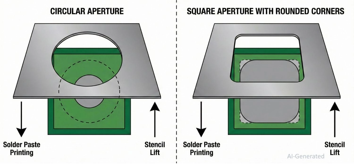
Figure: Comparing circular versus square stencil apertures for BGA solder paste printing.
Step 3: Accurate Component Placement
Once the paste is printed, the pick-and-place machine takes over. Modern machines use vision systems to recognize the array of solder balls on the bottom of the BGA. As the solder melts in the next step, the surface tension of the liquid metal naturally pulls the component into the center of the pad. This self-alignment capability corrects slightly off-center placements.
Step 4: Reflow Heating Process
The PCB travels through a reflow oven. The BGA soldering temperature profile must be tuned specifically for the thermal mass of the component:
Soak Zone: The board is held at a steady temperature (usually 150°C–180°C) for 60-120 seconds. This allows the flux to activate and remove oxides, and crucially, it ensures the entire BGA (center and edges) reaches the same temperature before the spike.
Reflow Zone: The temperature spikes above the melting point (Liquidus).
Time Above Liquidus (TAL): This is the critical parameter. The solder must stay liquid for 45–90 seconds.
- Too Long: The intermetallic layer becomes too thick, making the joint brittle.
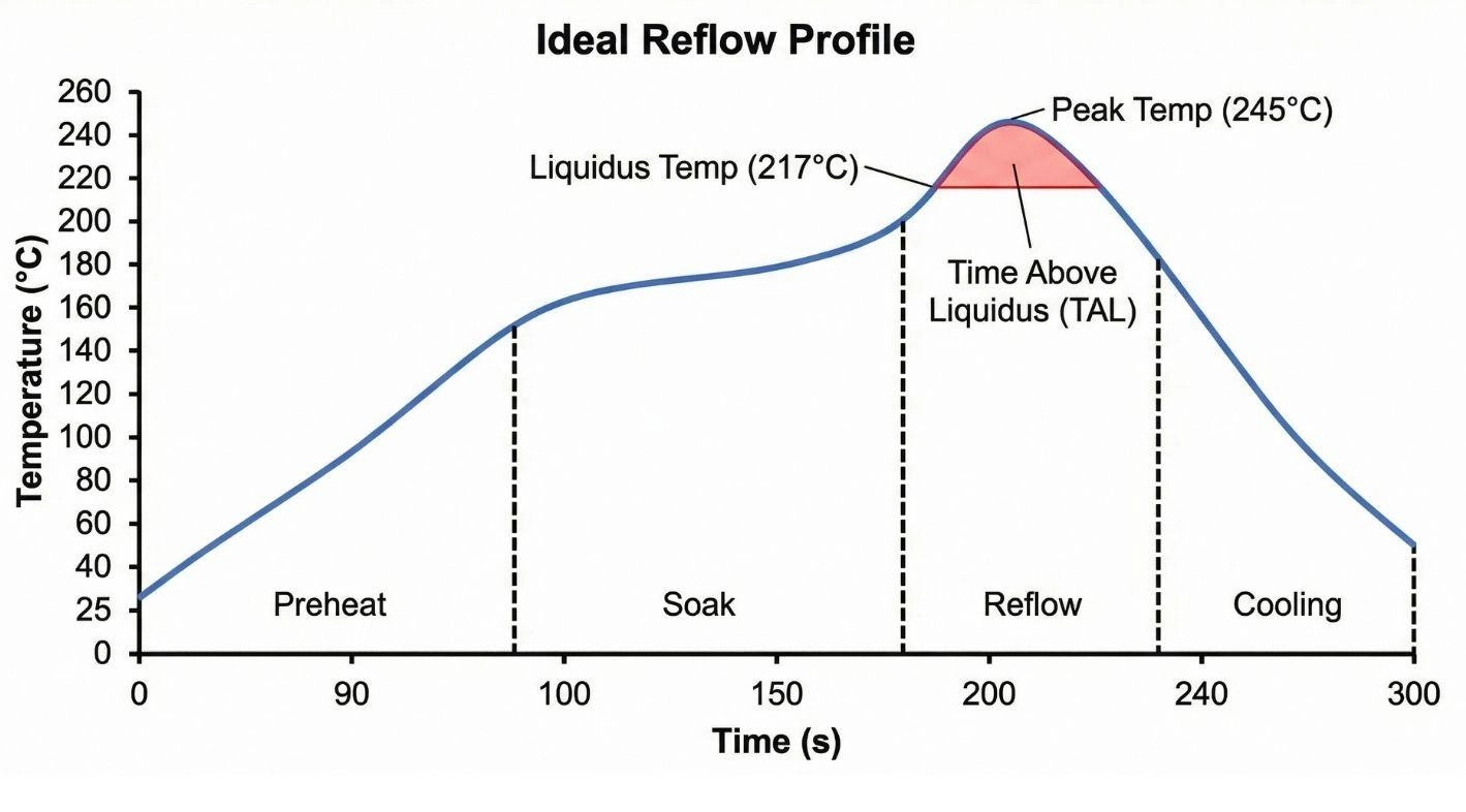
Figure: SMT reflow profile graph highlighting preheat, soak, and reflow zones for BGA soldering.
Step 5: Inspection and Quality Check
Because the joints are hidden, automated systems step in immediately after cooling to verify that the reflow process was successful, ensuring no shorts or voids exist beneath the package.
Tools and Equipment for BGA Soldering
High-quality assembly and repair require specialized BGA soldering tools.
BGA Rework Station
For any manual intervention, you need a dedicated BGA Rework Station. This combines top heating, bottom pre-heating, and precision alignment optics into a single unit, ensuring the exact reflow profile can be mimicked outside the main SMT oven.
Hot Air Rework Tools
A standard soldering iron cannot reach under a BGA. Hot air rework tools provide a focused flow of temperature-controlled air to melt the solder balls evenly. The nozzles used are shaped precisely to match the square footprint of the specific BGA chip being targeted.
Infrared Rework Machines
As an alternative to hot air, some advanced rework stations use Infrared (IR) heating. IR stations heat the component using infrared light waves, which can prevent the surrounding smaller components from being blown away by air currents, a common risk with hot air tools.
X-Ray Inspection Systems
Visual inspection can only verify the outer row of solder balls. To see the hidden rows, you need Automated X-Ray Inspection (AXI). Solder absorbs X-rays and appears dark, while the PCB is transparent, allowing technicians to spot internal defects easily.
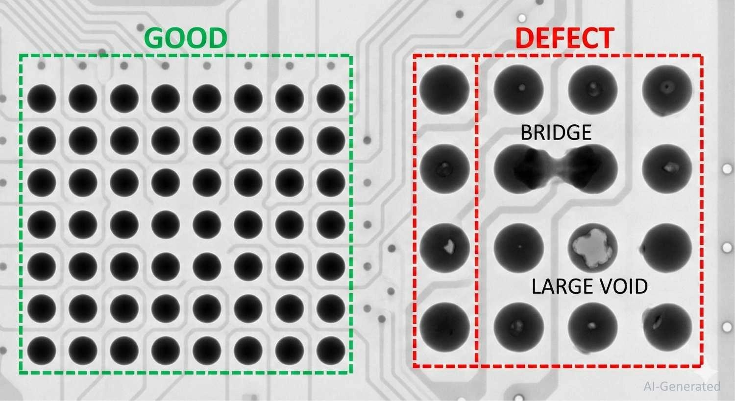
Figure: X-ray inspection image showing BGA solder balls with voiding and bridging defects.
Common Challenges in BGA Soldering
Even with automation, things can go wrong. Identifying these defects is the first step to fixing them.
Solder Voids
Solder voids are essentially air or gas bubbles trapped inside the solder ball.
- The Standard: According to IPC-A-610 Class 2, voids are acceptable if they occupy less than 25% of the X-ray image area of the ball.
- The Cause: Solder voids are often caused by flux outgassing. If the reflow profile ramps up too quickly, the flux solvent boils before it can escape, trapping gas inside the hardening metal.
Head-in-Pillow (HiP)
This is the nightmare of BGA assembly. In a HiP defect, the BGA solder ball melts, and the paste on the PCB melts, but they do not merge. The ball simply rests on top of the pillow of paste, creating an intermittent electrical connection that might pass a quick functional test but fail later.
- Root Cause: Usually caused by component warpage. The BGA corners lift up during heating, separating the ball from the paste. By the time it drops back down, the paste has oxidized and formed a "skin," preventing coalescence.
Bridging Between Balls
Bridging occurs when solder connects two adjacent pads.
- Cause: Often due to excessive solder paste deposition, low stencil tension, or placing the component with too much pressure, which squishes the paste out.
Misalignment During Reflow
Also known as the Head-in-Pillow (HiP) defect, this occurs when the BGA solder ball melts, and the paste melts, but they do not merge. The ball rests on top of the pillow of paste, creating an intermittent connection. It is usually caused by component warpage lifting the ball away from the paste during the heating cycle.
Pad Cratering
This is a mechanical failure where the copper pad is physically ripped out of the PCB laminate. It is rarely a soldering fault and usually a result of mechanical stress (bending the board) or thermal shock.
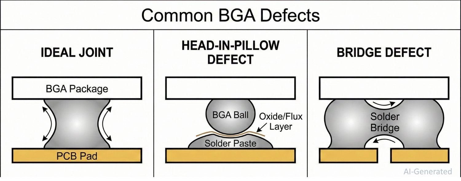
Figure: Showing Head-in-Pillow defect versus healthy solder joint and solder bridging.
Learn More: BGA Void Explained: Causes, IPC Standards, and Prevention
BGA Rework and Repair Techniques
When a defect is found, the component must be repaired using specific BGA soldering techniques.
BGA Reballing Process
If a BGA is removed, it cannot be simply placed back onto a board. It requires reballing - a labor-intensive process of removing old solder, applying fresh flux, and attaching new BGA solder balls using a specialized stencil fixture. Once reballed, the chip is ready to be reused.
Removing and Replacing BGA Chips
Removing a BGA requires applying tacky flux around the edges, setting the rework station to the exact melting temperature, and gently lifting the chip with a vacuum pen once the solder liquefies. After removal, the PCB pads must be carefully cleaned with desoldering braid before new paste is applied for the replacement chip.
Preventing Damage During Rework
Pre-heating is mandatory. You must use a bottom heater to bring the whole board to ~150°C. If you only blast the BGA with top heat, the local thermal expansion will warp the board and likely rip pads off.
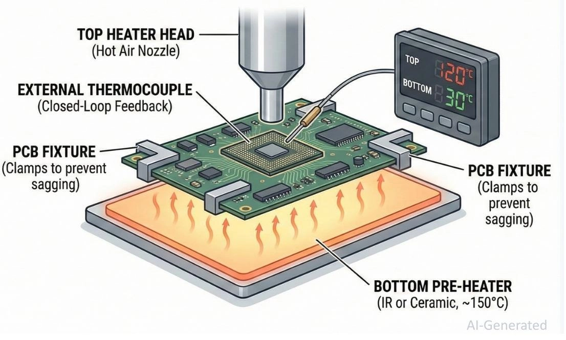
Figure: BGA rework station showing top nozzle, bottom pre-heater, PCB clamps, and temperature sensors.
The Risk: Manual rework puts high thermal stress on the component and the PCB. It is often safer and more cost-effective to order a few assembled prototypes from a professional service like JLCPCB rather than risking an expensive FPGA with a hand-held heat gun.
Learn More: BGA Rework Guide: Process, Tools, and Best Practices
BGA Soldering vs Other SMT Soldering Methods
BGA vs QFN Packages
Quad Flat No-leads (QFN) packages have metal pads around their bottom perimeter and a large thermal pad in the center. While easier to route than BGAs, QFNs are limited in pin count. Once you surpass 100 pins, the BGA structure (which uses the entire bottom area, not just the edges) becomes mandatory.
BGA vs QFP Packages
Quad Flat Packages (QFP) feature fragile "gull-wing" leads extending from the sides. They are easy to inspect visually, but take up massive amounts of board space and suffer from high inductance compared to BGAs.
Feature | Quad Flat Package (QFP) | Ball Grid Array (BGA) |
|---|---|---|
Pin Density | Low to Medium (Peripheral only) | High (Full area array) |
Inductance | High (Long leads) | Low (Short solder balls) |
Inspection | Visual / Optical Microscope | X-Ray Inspection Required |
Advantages of BGA Technology
Ultimately, BGA technology wins because of its unparalleled spatial efficiency, allowing engineers to pack immense processing power into shrinking form factors like smartphones and wearables. The package's natural self-centering abilities during the reflow process also forgive minor pick-and-place alignment errors, leading to higher manufacturing yields.
Furthermore, the robust thermal and electrical performance provided by the short, solid solder balls ensures superior heat dissipation to the PCB ground planes and significantly cleaner signal integrity for high-speed circuits like GPUs, CPUs, and FPGAs.
Professional PCB Assembly and BGA Soldering Services at JLCPCB
While manual rework is possible in a pinch, the reliability of automated assembly is unmatched. Hand-soldering puts high thermal stress on the component and the PCB.
It is always safer and more cost-effective to utilize a professional service.
JLCPCB’s PCB assembly service ensures your fine-pitch components are placed with perfect accuracy. Furthermore, X-ray inspection is not an optional add-on; it is a standard protocol for BGA assembly at JLCPCB, ensuring your high-density designs perform perfectly every time.
Best Practices for Reliable BGA Soldering
Beyond the standard process, here are three pro-tips from the factory floor to ensure success.
Proper Temperature Profiles
Don't guess the BGA soldering temperature. Professional profiling involves drilling a hole through a scrap PCB and attaching a thermocouple directly to a solder ball in the center of the grid. This ensures the innermost balls reach liquidus, not just the ones on the edge.
Accurate Component Alignment
Always place fiducial markers (local fiducials) near the corners of the BGA on your PCB design. This gives the pick-and-place machine a precise local reference to calculate the exact position of the pads, ensuring perfect alignment before reflow.
Using High-Quality Solder Paste
Solder Paste Hygiene is critical. Paste that has been on the stencil too long loses flux activity, which is a leading cause of Head-in-Pillow defects. Regular cleaning and using fresh paste are non-negotiable for reliable joints.
FAQ about BGA Soldering
Q: Is underfill always required for BGA components?
No, underfill - an epoxy injected under the BGA after reflow - is not required for most consumer electronics. It is primarily used for handheld devices (like smartphones) or automotive environments where the PCB is subject to frequent mechanical shock or vibration. Underfill relieves the stress on the solder joints during drops.
Q: Can I place BGAs on both sides of the PCB?
Yes, double-sided assembly is possible, but it adds complexity. Typically, the BGAs on the bottom side are reflowed first. During the second pass (top side), the bottom BGAs are held in place by the surface tension of the molten solder, provided the component weight does not exceed the surface tension limit (usually < 30g/in²).
Q: How do I clean flux residue from under a BGA?
Cleaning under a BGA is difficult because the "standoff height" (the gap between component and PCB) is extremely small. Standard washing often fails to penetrate this gap. For this reason, most BGA assembly lines use No-Clean Flux, which leaves a non-conductive, non-corrosive residue that does not require removal.
Q: Can a desoldered BGA be reused?
Technically, yes, but it cannot be simply placed back onto a board. It requires reballing - a labor-intensive process of removing old solder, applying fresh flux, and attaching new solder spheres using a specialized fixture. For inexpensive chips, it is usually more cost-effective to use a new component.
Q: Does using fine-pitch BGAs increase the bare PCB cost?
Yes. While the assembly cost increases due to X-ray requirements, the bare PCB cost often jumps significantly if the pitch drops below 0.5mm. At this scale, you often cannot route traces between pads on the top layer, forcing the use of HDI (High-Density Interconnect) technology, which involves blind/buried vias and extra lamination cycles.
Conclusion
BGA soldering is a sophisticated dance of chemistry, thermodynamics, and optics. It allows us to build powerful, compact devices, but it demands respect for the process. From designing the correct apertures to fine-tuning the reflow profile and verifying with X-ray, every step matters.
While manual rework is possible in a pinch, the reliability of automated assembly is unmatched. Whether you are prototyping a new IoT device or scaling up production, understanding these principles ensures your high-density designs perform perfectly every time.
Ready to move to high-density designs? Trust your BGA projects to JLCPCB's PCB assembly service, where advanced X-ray inspection and precise reflow profiling come standard.
Popular Articles
• Common PCB Assembly Methods and Soldering Techniques Explained
• What Is BGA Void? Causes, IPC Limits, and Solutions
• SMD Soldering Tools You Need: Complete Guide from Beginner to Pro
• Reflow Soldering: Everything You Need to Know
• SMT Assembly Process Explained and Equipment Used: A Step-by-Step Guide to PCBA Manufacturing
Keep Learning
12 Professional Soldering Tips and Tricks Every Beginner Should Know
Soldering is not merely "gluing" metal; it is a metallurgical process that creates an intermetallic compound (IMC). This molecular bond ensures the electrical and mechanical integrity of your device. A poor joint might pass a quick visual check but will inevitably fail under vibration or thermal stress, leading to "ghost" bugs and hardware failures. These soldering tips and tricks focus on practical, repeatable techniques used in professional electronics soldering—from correct heat transfer and flux u......
Solder Melting Point Guide: Chart, Alloy Types, and Reflow Considerations
In the precise world of electronics manufacturing, a difference of just a few degrees can mean the distinction between a perfect, reliable solder joint and a catastrophic "cold" joint failure. While many hobbyists view soldering simply as "melting metal to stick things together," professional PCB assembly requires a nuanced understanding of thermodynamics. The solder melting point is not simply a single value listed in a datasheet; it is a decisive limit that determines the choice of components, the s......
The Ultimate Guide to Solder Flux: Everything You Should Know Before Soldering PCB
Soldering is needed to make almost all electronic devices. Adding solder alone won't make a joint that is strong, clean, and sound from a metallurgical point of view. Solder flux is a very important part of the process that comes in here. If you want to do your job better and make it more reliable, you need to know a lot about soldering flux, whether you're an engineer, a professional technician, or just a hobbyist. This article goes into a lot of detail about solder flux, including what it is, how it......
Common PCB Assembly Methods and Soldering Techniques Explained
Whether you're designing your first prototype or scaling up to production, understanding PCB assembly methods and soldering techniques is crucial to achieving reliable, high-performance circuit boards. Modern PCBA primarily relies on Surface Mount Technology (SMT) and Through-Hole Technology (THT)—each offering unique advantages for component density, durability, and manufacturability. In this guide, we'll break down the major PCB assembly methods, key soldering techniques such as reflow and wave sold......
Flex PCB Assembly Guide: Process, Challenges, and Solutions
Flexible Printed Circuit Boards (Flex PCBs) are the foundational technology enabling the compact, innovative design of modern electronics. Because of their ability to bend and fold, they power devices from smart wearables to compact medical instruments where traditional rigid printed circuit boards (Rigid PCBs) can't be used. Achieving a functional electronic circuit from the raw plastic film demands special expertise, with flexible PCB assembly (FPCA) representing the crucial final step in this trans......
SMD Rework Guide: Tools, Temperatures, and Techniques That Prevent PCB Damage
From replacing a burned regulator to correcting wrong component values or removing solder bridges on fine-pitch ICs, SMD rework is an essential skill in electronics manufacturing and prototyping. It allows engineers to repair assembly defects, implement design changes, and recover valuable PCBs without the cost and delay of building new boards. In this guide, you will learn: What SMD rework is Common rework scenarios Tools and temperatures Safe removal and installation Package-specific techniques Real......