PCB Component Placement: A Practical Guide to Clean, Routable Layout
10 min
- Introduction
- Top 5 Golden Rules for PCB Component Placement
- PCB Placement Guidelines: Start with Functional Zoning
- A Practical PCB Component Placement Sequence
- PCB Component Placement Guidelines for Signal Integrity
- PCB Layout Component Placement Guidelines for Signal Flow
- Thermal and Mechanical Constraints in PCB Layout
- PCB Component Placement Guidelines for Manufacturability (DFM)
- Common PCB Placement Mistakes That Cause Routing and EMC Problems
- FAQ about PCB Component Placement
Key Takeaways
Functional Zoning First: Group circuits by function (power, digital, analog, RF) before placing any component to minimize interference and simplify routing.
Lock Down Mechanical Constraints: Connectors, mounting holes, and displays are difficult or impossible to reposition later in the design process.
Decoupling Capacitors Close to Power Pins: Even 10 mm of extra trace adds parasitic inductance that degrades high-frequency noise filtering.
Follow a Structured Placement Sequence: Mechanical constraints, key ICs, supporting passives, secondary components, then a placement sanity check before any routing begins.
Separate Noisy and Sensitive Circuits: Keep DC-DC converters, motor drivers, and clock oscillators physically away from ADC inputs, sensor interfaces, and RF receivers.
Align Components Along the Signal Flow Axis: Arrange components from input to output to minimize trace length, reduce reflections, and simplify debugging.
Consider DFM from the Start: Consistent component orientation, adequate spacing for pick-and-place, and clearance for wave soldering improve assembly yield and reduce defects.
Introduction
PCB routing often receives the most attention during board design, but placement decisions usually determine whether a layout will be easy or difficult to route. Component placement influences signal integrity, EMI performance, thermal behaviour, and manufacturability long before the first trace is drawn.
Modern embedded systems frequently combine power converters, microcontrollers, communication interfaces, analog circuits, and RF subsystems on a single PCB. Effective component placement organizes these functions to reduce routing complexity, minimize interference, and improve first-pass design success.
Top 5 Golden Rules for PCB Component Placement
-
Functional Zone Planning Before Component Placement
Plan the circuit according to the logic, power, and analog functions.
-
Placement of Connector and Mechanical Constraints First
Fix the physical constraints of the circuit first.
-
Related Circuits Should Be Placed Close Together
Reduce the physical spacing of the circuits.
-
Decoupling Capacitors Next to the Power Pins
It is very important for power distribution network stability.
-
Validate the Placement Before Starting Routing
Sanity checking needs to be performed to have free routing channels.
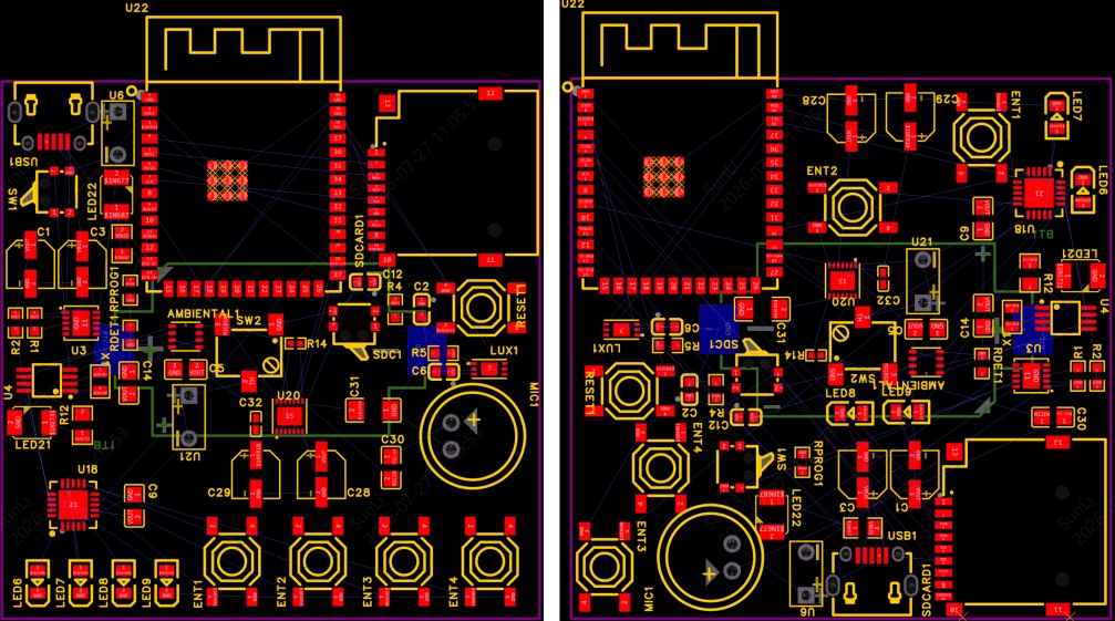
Comparison of organized and poor PCB component placement before routing
PCB Placement Guidelines: Start with Functional Zoning
Before placing individual components, divide the PCB into logical functional areas. This process, functional zoning, creates the foundation for a clean, reliable, and highly routable layout.
Typical zones include:
- Power circuits
- Digital circuits
- Analog circuits
- Communication interfaces
- RF sections, if applicable
Grouping related circuits together minimizes interference and helps maintain a logical signal path throughout the board.
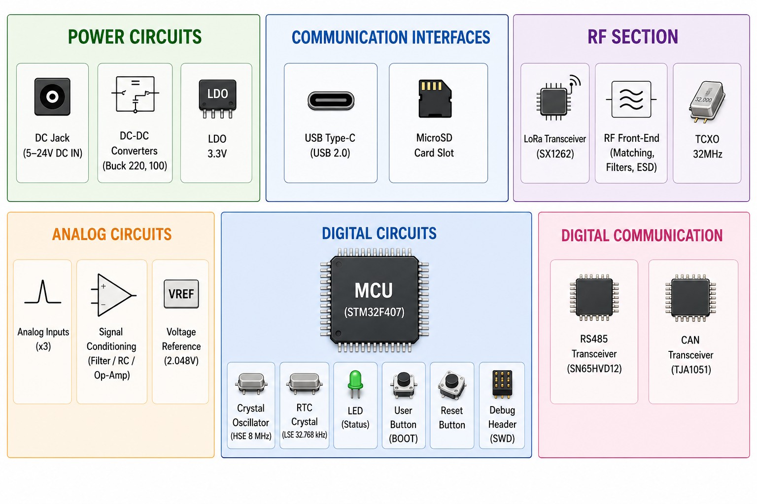
Block diagram showing power, digital, analog, communication, and RF zones
Why Skipping Zoning Creates Problems Later
Without proper segregation of analog, digital and power circuits, design teams will frequently run into the following issues:
- Crosstalk among signals
- Routing congestion
- Grounding return path issues
- Emissions of electromagnetic interference
- Debugging challenges
Placing sensitive analog inputs near switching regulators increases the likelihood of noise coupling and measurement errors. Many signal integrity, EMI, and routing problems originate during placement and become much harder to resolve later in the design process.
How to Define Zone Boundaries
Start by reviewing the schematic and identifying major functional blocks. The goal is to arrange circuits so that power and signals flow naturally through the board.
A practical layout often follows this sequence:
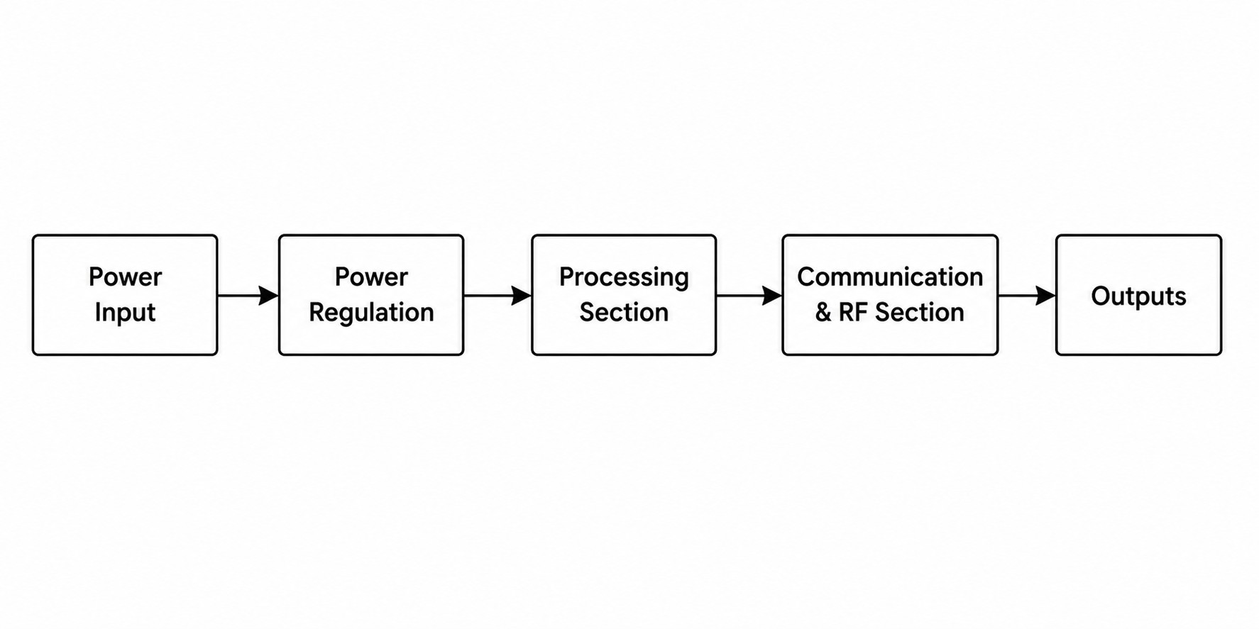
This arrangement minimizes unnecessary signal crossings and simplifies routing between functional blocks.
After establishing the overall flow, place each functional block into its own dedicated zone. This creates clear routing channels and reduces interference between unrelated circuits.
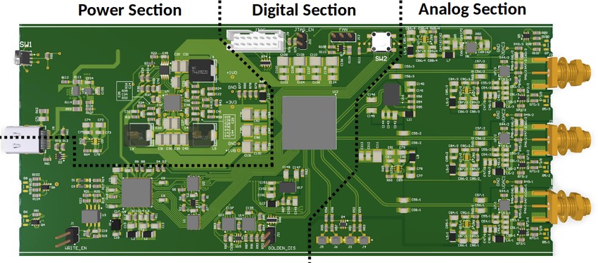
PCB layout separating power, digital, communication, and RF sections
Isolation Distance Between Noisy and Sensitive Circuits
Circuits do not create equal amounts of electrical noise. Some components will inherently generate switching transients and electromagnetic interference, whereas some will need a low-noise environment to function.
Some common sources of noise include:
- DC-DC converters
- Motor drivers
- Clock oscillators
- High-current switching circuits
Sensitive circuits include:
- ADC inputs
- Sensor interfaces
- Precision references
- RF receivers
Whenever possible, maintain physical separation between noisy and sensitive circuits. Increasing physical separation reduces capacitive and inductive coupling between noisy and sensitive circuits.
Once functional zones are established, the next step is determining how components should be arranged within each zone.
A Practical PCB Component Placement Sequence
A structured workflow reduces placement errors and prevents routing difficulties later in the design process.
-
Lock Down Mechanical Constraints First
Begin with components whose locations are fixed by the enclosure or product requirements. These typically include connectors, mounting holes, displays, buttons, and antennas. Because these components are constrained by mechanical requirements, they are usually difficult or impossible to move later.
-
Position Key ICs and High-Power Devices
After mechanical elements are fixed, place the primary active devices. Examples include microcontrollers, processors, FPGAs, power management ICs, and motor drivers. Keep these devices close to the circuits they communicate with most frequently. This reduces trace length, improves signal integrity, and simplifies routing.
-
Place Supporting Passives Around Each IC
Every major IC depends on supporting components such as decoupling capacitors, pull-up resistors, feedback networks, and crystal circuits. Place these components immediately after positioning the IC. Waiting until later often results in longer connections and reduced performance.
-
Fill Secondary and Remaining Components
After critical circuits are complete, place secondary components such as LEDs, test points, configuration jumpers, and optional circuits.
-
Run a Placement Sanity Check Before Routing
Before routing begins, review functional zoning, signal flow, component spacing, thermal considerations, and connector accessibility. A placement review at this stage can prevent costly redesigns later.
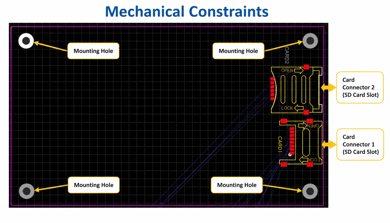
EasyEDA layout showing connectors, mounting holes, and board outline
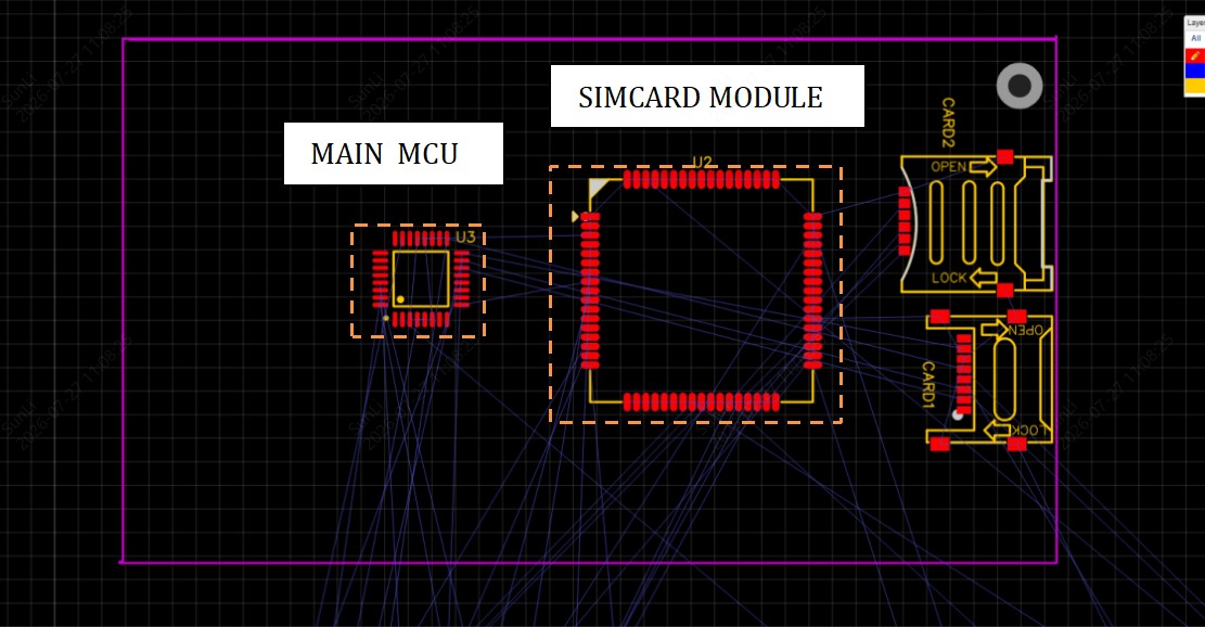
EasyEDA PCB layout showing microcontroller and critical IC placement
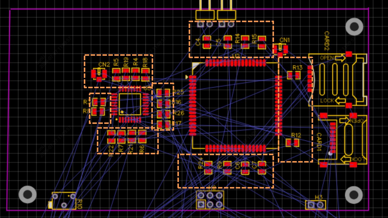
EasyEDA PCB layout with decoupling capacitors and supporting passives
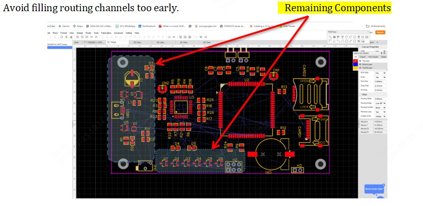
PCB layout showing LEDs, jumpers, and secondary components
By following a structured placement sequence, designers create a layout that is easier to route and more likely to perform correctly on the first revision.
PCB Component Placement Guidelines for Signal Integrity
Good PCB component placement improves signal integrity before routing even starts. A compact power layout reduces noise, lowers impedance, and keeps the power distribution network stable. Placement decisions establish the foundation for signal integrity before routing begins.
Compact Power Layout and the Short-Path Principle
For power traces carrying significant current, conductor width should be selected based on the expected current and allowable temperature rise. IPC-2152 (Standard for Determining Current-Carrying Capacity in Printed Board Design) provides widely accepted guidance for determining appropriate PCB trace widths.
Decoupling Capacitor Placement Strategy
Place every decoupling capacitor beside its power pin. Even a 10 mm trace adds inductance and reduces its effectiveness at high frequencies.
Routing Decoupling Caps to Ground
Give each capacitor a short, direct path to the ground plane. A long ground connection increases loop area and allows more noise to circulate.
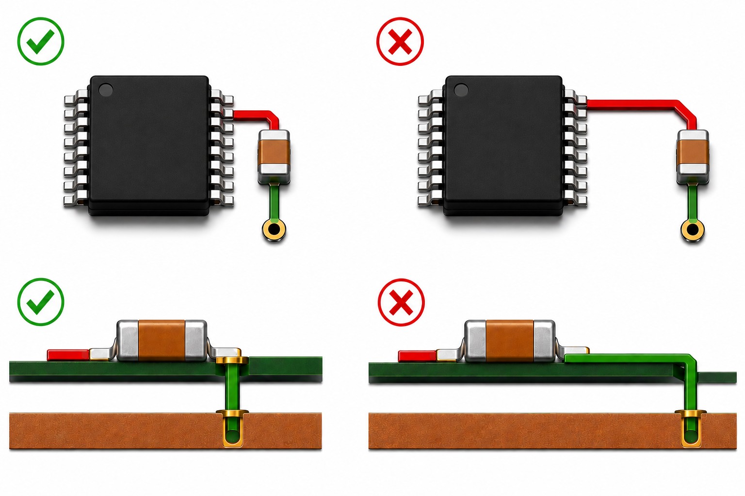
Proper and improper decoupling capacitor placement for stable power delivery
PCB Layout Component Placement Guidelines for Signal Flow
Signal paths should follow a logical flow from input, processing, and output stages. Keeping related components close together shortens trace length, reduces reflections, and makes the board easier to route and debug.
Aligning Components Along the Signal Axis
Arrange components from input to output whenever possible. Straight signal paths are easier to route and improve signal quality.
Distance Control Between High-Speed Connectors and ICs
Keep USB, Ethernet, HDMI, and similar connectors close to the controller or processor. Short traces reduce delay, reflections, and EMI.
Handling Cross-Zone Routing
Avoid routing signals through analog, RF, or power sections unless necessary. Crossing functional zones increases noise and makes debugging more difficult.
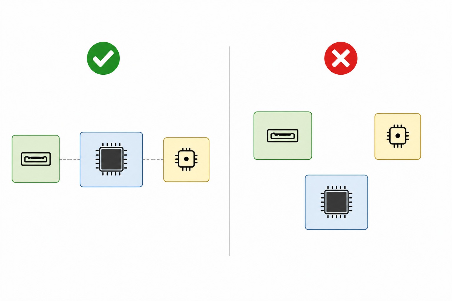
Comparison of optimized and poor PCB component placement based on signal flow and component proximity
Thermal and Mechanical Constraints in PCB Layout
A reliable PCB depends on more than electrical design. Heat, mechanical stress, and safety spacing all affect long-term performance and reliability.
Positioning Heat-Generating Components for Airflow
Place regulators, MOSFETs, and other hot components where airflow is available. Keep them away from temperature-sensitive devices.
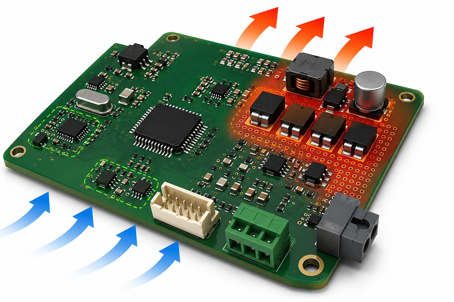
Thermal-aware PCB component placement where regulators and MOSFETs are isolated from sensitive analog and timing circuits to improve reliability
Creepage and Clearance Requirements
Maintain proper creepage and clearance distances between high-voltage circuits to improve electrical safety and reduce the risk of arcing. IPC-2221 (Generic Standard on Printed Board Design) provides design guidelines for determining minimum spacing requirements based on operating voltage and environmental conditions.
Isolating Stress-Sensitive Components
Keep crystals, sensors, and precision references away from mounting holes and board edges. Mechanical stress can affect their accuracy.
PCB Component Placement Guidelines for Manufacturability (DFM)
A good layout should also be easy to manufacture. Proper component orientation, spacing, and placement improve assembly quality and reduce production defects.
Component Orientation for Wave Soldering
Place similar components in the same direction whenever possible. This improves solder quality and simplifies inspection.
Shadow Effect: How Tall Components Block Solder Access
Avoid placing tall components in front of smaller ones during wave soldering. They can block solder flow and create weak joints.
Placement Spacing for Pick-and-Place Efficiency and Reflow Quality
Leave enough space between components for assembly machines. Proper spacing also improves reflow results and makes future repairs easier.
Common PCB Placement Mistakes That Cause Routing and EMC Problems
Many routing and EMC problems begin during placement. Following PCB component placement guidelines early helps reduce noise, improve routing, and avoid unnecessary board revisions.
Misplaced Decoupling Caps and PDN Impedance
A decoupling capacitor should always sit close to the power pin. Long traces increase PDN impedance and reduce noise filtering.
Connector Signal Paths Crossing Functional Zones
Do not force connector signals to cross multiple functional areas. Longer paths increase routing complexity and EMI.
Passive Component Clutter That Blocks Routing
Avoid placing every resistor and capacitor at the beginning. Leave routing space for important signals before filling the remaining areas.
Did You Know?
Nearly 30% of EMI-related layout problems are caused by poor component placement before routing begins. In the JLCPCB Layout Service, DFM checks are performed during the placement stage to catch these issues before they become expensive PCB respins.
Let JLCPCB engineers handle your full layout—from optimal component placement to EMI-free routing.
Get a Quote
FAQ about PCB Component Placement
Q: How should the ground plane be placed?
A continuous ground plane should generally be placed on an inner layer beneath signals to minimize loop area.
Q: Can components be placed on the bottom side?
Yes, but keep in mind that double-sided assembly requires two reflow passes, which increases cost.
Q: What is the biggest mistake in placement?
Ignoring functional zones. Without them, boards end up with spaghetti routing that is impossible to stabilize for EMI.
Q: Does spacing matter for soldering?
Absolutely. Tight spacing leads to bridging and makes solder joint inspection difficult.
Q: Should high-speed traces be placed near the board edge?
In many designs, routing high-speed traces near the board edge is avoided because edge coupling can increase radiated emissions.
Conclusion: PCB Component Placement Guidelines
Successful PCB Component Placement is about short signal paths, compact power loops, good thermal management, and simple routing. Following good placement guidelines improves signal integrity, reduces EMI, and increases first-pass success.
Keep Learning
How to Design a PCB Board: 5 Steps from Schematic to Layout
Designing a PCB board means turning a validated schematic into a manufacturable layout: start with a clean schematic, place components by function and signal flow, route traces with signal integrity in mind, then manage heat and EMI before running design rule checks and exporting Gerber files. Free tools like EasyEDA cover the complete workflow. This guide explains the layout guidelines that matter at each stage, from schematic preparation to thermal management. Introduction Printed circuit board (PCB......
EMI vs EMC: A Full Guide to Detailed Comparison
EMI (electromagnetic interference) is unwanted electromagnetic energy that degrades the performance of electronic devices. EMC (electromagnetic compatibility) is the design discipline that ensures a device works properly in its electromagnetic environment without disturbing other equipment. For PCB designers, the distinction matters because every layout decision — stackup, grounding, component placement, and trace routing — determines how much EMI a board emits and how well it survives it. Introductio......
PCB Design Guidelines 101: Placement and Routing
Welcome to the second article in our PCB design guidelines series. In this article, we will explore the essential PCB design guidelines that are crucial for achieving optimal PCB design performance and functionality. Whether you're an electronics enthusiast, hobbyist, engineer, student, or professional in the field, understanding these guidelines will empower you to create high-quality PCB designs. In this article we will explore foundational principles and best practices in designing printed circuit ......
BGA PCB Design Complete Guide: Layout and Routing Guidelines
Key Takeaways Define pad type first: Always confirm SMD or NSMD pad strategy before routing BGA fanout. NSMD is generally preferred for better solder joint formation, while SMD suits very small pads or tight mask registration. Match the process to the pitch: 0.8 mm BGAs work with dog-bone fanout and standard vias; 0.5 mm BGAs typically need via-in-pad or HDI routing. Picking the right via strategy early saves layers and cost. Place decoupling capacitors on the bottom side: Mount MLCCs directly under t......
The Ultimate Guide to PCB Layout Design
Printed Circuit Board (PCB) layout design is the foundation of any electronic device, from simple gadgets to highly complex systems. PCB layout design is the process of arranging electronic components and routing connections on a board to create a functional and efficient circuit. The goal is to achieve the smallest possible footprint while maintaining signal integrity and ensuring thermal and electrical performance. There is a lot that goes into any engineered circuit board design, from a basic print......
PCB Layout Guidelines for USB Type-C
Introduction to USB Type-C USB Type-C (USB-C) is a universal connection standard used for device connectivity and charging. As the latest evolution of USB interface, USB-C comes with several advantages, including reversible plug orientation, higher data transfer rates, and power output capabilities. Additionally, USB Type-C can transmit audio and video signals and is compatible with various accessories such as monitors, external storage devices, and chargers. Features of USB Type-C Reversible Plug Ori......