5 PCB Board Layout Design Rules for Manufacturing Success
9 min
- Why PCB Board Layout Design Matters for Manufacturing?
- Rule 1: Define Clear PCB Layout Rules Before You Start
- Rule 2: Optimize Component Placement in Layout PCB Design
- Rule 3: Follow Efficient Trace Routing
- Rule 4: Layout PCB Design for Manufacturability
- Rule 5: Validate Your PCB Layout Design Drawing Before Production
- FAQ about 5 PCB Board Layout Design Rules for Manufacturing Success
Key Takeaways
Rule-driven PCB layout: Define layout rules before placement begins to reduce revision cycles and fabrication risk.
Optimized component placement: Group functional blocks, place critical components first, and maintain assembly-friendly spacing for reliable manufacturing.
Efficient trace routing: Keep traces short and direct, control width and spacing, and avoid crosstalk and EMI to ensure signal integrity.
Design for manufacturability: Follow manufacturer limits, add fiducials and test points, and avoid common layout mistakes such as insufficient spacing or incorrect pad definitions.
Final validation: Run full DRC, review Gerber outputs, and prototype before mass production to confirm fabrication readiness.
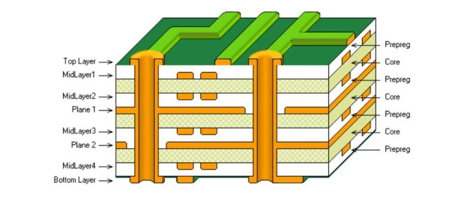
Why PCB Board Layout Design Matters for Manufacturing?
Physical circuit layout determines how an electronic design becomes a manufacturable product. PCB layout translates electrical intent into precise board geometry. It defines copper spacing, drill placement, and assembly alignment, while the distribution of copper across layers influences current handling, thermal balance, and fabrication stability.
Many manufacturing defects originate from layout errors. Poor design can lead to solder defects, impedance mismatches, and assembly misalignment. These layout decisions ultimately impact yield, cost, and production stability. Following a few key rules helps reduce downstream costs during fabrication and assembly by controlling the geometry and volume of conductive material.
From Schematic to PCB Layout Designing
Schematic capture defines electrical relationships between components. Printed circuit layout converts those relationships into physical placement and routing. The spacing, trace geometry, and assembly compatibility is determined by the layout of a PCB design.
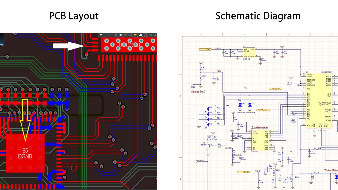
A structured PCB board layout design process reduces iteration cycles and fabrication risk. Professional layout services from JLCPCB align electrical design with manufacturing constraints.
How Poor PCB Design Layout Impacts Production
Poor PCB design layout creates assembly failures and electrical instability. Layout PCB design errors lead to solder bridging, insufficient clearance, and impedance variation. PCB layout designing mistakes increase rework and scrap rates.
The incorrect design layout and PCB geometry disrupt the automated assembly processes. Inconsistent spacing affects pick-and-place accuracy and solder joint formation. Manufacturing yield decreases due to avoidable layout issues.
Rule 1: Define Clear PCB Layout Rules Before You Start
Early rule definition drives the entire PCB layout process—governing spacing, trace width, and placement constraints that ensure electrical performance and manufacturability. Defined upfront, these rules reduce revision cycles, prevent costly redesigns, and maintain a fabrication-ready workflow throughout.
Set Design Constraints Based on Manufacturing Capabilities
Manufacturing limits determine critical parameters such as minimum trace width, spacing, and drill sizes. The layout must align with fabrication tolerances, copper thickness, via dimensions, and layer count requirements.
It should also account for assembly needs, including proper component spacing and pad geometry. Ignoring these constraints often leads to rejected boards or production issues. Aligning design decisions with manufacturer specifications ensures smoother fabrication and assembly.
Use DRC and Stack-up Planning Early
Design Rule Check (DRC) systems automatically enforce layout constraints and help catch spacing, clearance, and connectivity issues early in the process. This reduces errors before generating fabrication outputs.
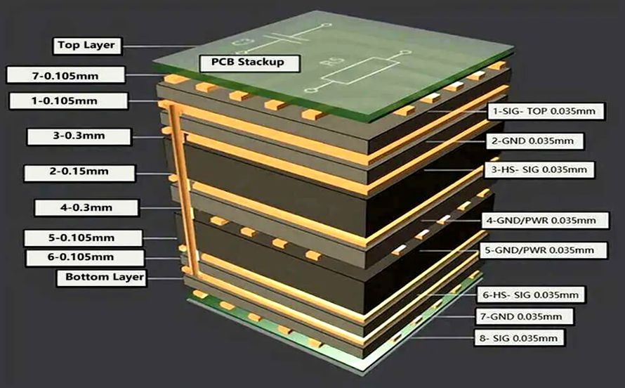
Stack-up planning defines the board’s layer structure and dielectric thickness, which directly impacts impedance control and signal integrity. Establishing the stack-up early improves overall design accuracy and helps avoid performance issues later in development.
Rule 2: Optimize Component Placement in Layout PCB Design
Component placement forms the structural foundation of PCB layout, preceding routing to optimize signal paths, return continuity, and assembly feasibility. Functional grouping and controlled spacing reduce routing complexity, minimize signal coupling, and maintain balanced copper distribution across layers.
Place Critical Components First
Critical components such as processors, memory, and power regulators should be positioned based on signal requirements. High-speed devices are best placed close to their associated circuits to minimise delays.
Keeping interconnect distances short between key nodes improves overall accuracy and performance, while priority-based placement ensures the most important signals are handled efficiently.
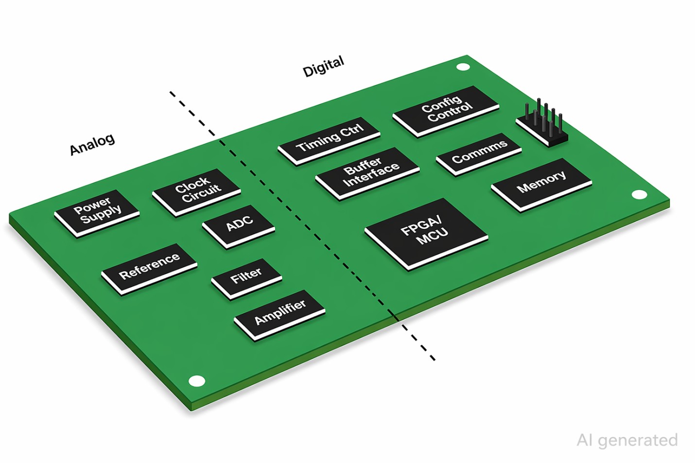
Group Functional Blocks and Separate Noise Sources
Functional grouping organises circuits by their roles, such as analog, digital, and power sections. Clear separation between these zones helps reduce interference.
Isolating noise-generating components from sensitive circuits improves signal integrity and overall system stability. Structured grouping ensures cleaner performance across the board.
Ensure Assembly-Friendly Spacing and Orientation
Component spacing directly affects assembly precision and solder quality. Maintaining consistent spacing supports reliable manufacturing.
Proper alignment and orientation also ensure compatibility with automated placement and soldering processes. Following these practices reduces placement errors and improves overall assembly yield.
Rule 3: Follow Efficient Trace Routing
Trace routing plays a key role in electrical performance and manufacturing reliability. Routing decisions define signal paths, influencing impedance, EMI, and thermal distribution across the board.
Poor routing can lead to signal distortion and electromagnetic interference. Maintaining consistent geometry throughout the layout helps ensure stable signal transmission and overall performance.
Keep Traces Short, Direct, and Consistent
Short traces reduce signal delay and distortion. Minimising unnecessary routing length and keeping paths direct between components improves efficiency.
Avoiding sharp turns and discontinuities further enhances signal integrity. Consistent routing helps maintain stable waveform behaviour across the design.
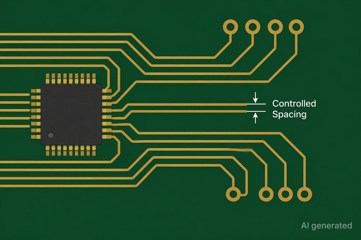
Control Trace Width and Spacing
Trace width determines current capacity and impedance, so it must be calculated based on electrical requirements. Proper spacing is equally important to prevent short circuits.
Avoiding spacing violations ensures manufacturability, while consistent dimensions support reliable electrical performance and proper clearance across layers.
Avoid Crosstalk and EMI Issues
Parallel traces can cause electromagnetic coupling between signals. Reducing parallel routing length and increasing spacing between high-speed traces helps limit interference.
Using ground planes to shield sensitive signals further reduces EMI. Controlled routing and proper isolation improve overall signal integrity.
Rule 4: Layout PCB Design for Manufacturability
Manufacturability determines whether a design can move smoothly into production. The layout must align with both fabrication and assembly processes, as it directly impacts yield and overall cost.
It should also account for equipment capabilities and process limits. Focusing on repeatable manufacturing performance ensures consistent output and reduces the risk of production issues.
Follow Manufacturer Limits and Standards
Manufacturers set limits for trace width, spacing, and drill size, and the design must stay within these boundaries. Aligning with fabrication capabilities is essential for successful production.
Exceeding these limits often leads to failed boards. Following established industry standards ensures reliability and helps maintain consistent, manufacturable geometry.
Add Fiducials and Test Points
Fiducials support accurate alignment during automated assembly, improving placement precision.
Test points enable electrical validation after assembly by providing accessible nodes for measurement. Including them makes debugging and verification more efficient.
Avoid Common Manufacturing Mistakes
Manufacturing defects often originate from layout-level inaccuracies. Design layout pcb decisions influence assembly yield and production repeatability. Error prevention at this stage reduces downstream rework and process instability.
Common Manufacturing Mistakes
- Insufficient Spacing: Tight copper spacing increases the risk of short circuits during soldering. Clearance violations affect solder flow and create bridging defects.
- Missing Solder Mask Clearance: Incorrect mask expansion exposes unintended copper areas. Mask misalignment leads to solder bridging and pad contamination.
- Incorrect Pad And Footprint Definitions: Improper pad geometry affects component seating and solder joint reliability. Footprint mismatch leads to placement errors during assembly.
- Poor Copper Separation: Inadequate isolation between nets increases electrical interference and shorting risk. Controlled separation maintains signal integrity and safety margins.
- Uneven Solder Mask Coverage: Inconsistent mask application exposes traces and reduces protection. Uniform coverage stabilizes solder behavior during reflow.
Structured error prevention improves manufacturability and stabilizes production output. Consistent rule application across layout PCB design reduces defect rates and enhances assembly reliability.
Rule 5: Validate Your PCB Layout Design Drawing Before Production
Final validation confirms fabrication readiness by verifying geometry, connectivity, and manufacturing constraints across the layout. Review of Gerber data, drill files, and layer mapping ensures alignment between physical design and electrical intent, reducing rework and improving yield.
Run Full Design Rule Check (DRC)
DRC verifies spacing, clearance, and connectivity to ensure rule compliance before fabrication.
Issues identified during this stage can be corrected early, improving overall accuracy. Automated checks help ensure the design meets all required constraints.
Review Gerber Files and Manufacturing Outputs
Gerber files represent the final manufacturing data and must be carefully reviewed. This step ensures proper layer alignment and completeness.
Reviewing outputs helps detect missing or incorrect data, including drill and copper layers, preventing errors during fabrication.
Prototype and Iterate Before Mass Production
Prototyping tests the design under real conditions, helping identify both functional and manufacturing issues.
Small batch testing allows for adjustments and refinement before full production. Iteration at this stage reduces risk and improves final output quality.

Build Manufacturing-Ready PCB Layout Designs from the Start
PCB board layout design follows a structured process that links each stage of development. Rule definition establishes constraints that guide placement, routing, and manufacturability decisions. Layout PCB design organizes components and copper distribution for stable electrical behavior. Routing then controls signal paths, impedance, and interference across the board.
Design for manufacturability aligns PCB layout with fabrication limits and assembly processes. Final verification confirms that all outputs match production requirements and electrical intent. These stages form a continuous workflow that reduces errors and stabilizes production yield.
FAQ about 5 PCB Board Layout Design Rules for Manufacturing Success
Q: What Causes PCB Manufacturing Failures Most Often?
Manufacturing failures often originate from PCB board layout design errors. Incorrect spacing, poor routing, and missing constraints lead to defects. Early rule definition reduces these risks.
Q: How Early Should PCB Design Layout Rules Be Defined?
PCB design layout rules must be defined before placement begins. Early constraints guide routing and manufacturability decisions. Late rule definition increases revision cost.
Q: Why Does Component Placement Affect PCB Manufacturing?
Placement determines spacing, routing paths, and assembly alignment. PCB board layout design relies on correct placement for manufacturability. Poor placement leads to solder defects and routing issues.
Q: What Is the Role of Gerber File Verification?
Gerber verification confirms that manufacturing data matches design intent. PCB design layout requires accurate output files for fabrication. Errors in Gerber files lead to production failure.
Q: How Does PCB Layout Designing Influence Cost?
PCB layout design affects material usage and production yield. Poor design increases rework and scrap rates. An efficient layout reduces manufacturing cost.
Keep Learning
Rigid Flex PCB Stackup Design: The Complete Guide 2026
Key Takeaways Adhesiveless Polyimide Cores: Cores should be made from adhesiveless polyimide laminates to eliminate inner-layer separation and plated through-hole (PTH) barrel cracking caused by the high Z-axis coefficient of thermal expansion (CTE) of acrylic adhesives. Rolled-Annealed Copper: Use rolled-annealed (RA) copper anywhere the board is designed to bend. Unlike electrodeposited (ED) copper, RA copper features a lamellar grain structure that withstands approximately 20–40% elongation without......
5 PCB Board Layout Design Rules for Manufacturing Success
Key Takeaways Rule-driven PCB layout: Define layout rules before placement begins to reduce revision cycles and fabrication risk. Optimized component placement: Group functional blocks, place critical components first, and maintain assembly-friendly spacing for reliable manufacturing. Efficient trace routing: Keep traces short and direct, control width and spacing, and avoid crosstalk and EMI to ensure signal integrity. Design for manufacturability: Follow manufacturer limits, add fiducials and test p......
How to Prepare PCB Drawings for Fabrication Services?
You already know the frustration of sending a PCB design for fabrication and having it come back with an "on-hold" notice. The drawing stage is where the real headaches start. You can have a perfect simulation, but if your documentation doesn't translate to the factory floor, it’s just expensive scrap metal. Creating a high-quality PCB drawing is essentially building a bridge. On one side, you have your theoretical circuit. On the other hand, you have a physical, high-performing product. The transitio......
How to Choose the Best Printed Circuit Board Layout Services
A high-quality schematic is just one part of the challenge in electronic design. After the schematic design, you need to convert that schematic into a functioning printed circuit board (PCB). An incorrect layout of the PCB can degrade a design's performance, causing many issues like electromagnetic interference (EMI), signal integrity (SI) issues, overheating, or, if it gets that far, a board that cannot be manufactured. So how does an engineer, hobbyist, or project manager figure out the market and c......
How to Use IPC Standards to Optimize Your PCB Layout
Designing a PCB is more than just connecting components on a board—it’s about creating a robust, reliable, and manufacturable design that meets industry standards. That’s where IPC standards come in. The IPC standards are among the most widely accepted and important standards for PCB design and manufacturing. Whether you work in electronics design, or manufacturing. IPC standards will influence how a designer creates their board and how they will prepare it for production in different industries. Thes......
PCB Board Layout in Modern Electronic Design
Printed circuit board (PCB) layout is crucial to build current electronic design. Among the multiple components affecting the dependability, efficiency, and performance of an electrical circuit is one of them. Apart from connecting several electrical components, the arrangement improves signal integrity, reduces noise, and controls temperature. The value of PCB board layout, the best design techniques, and the most crucial considerations for PCB layout construction will be discussed in this article. W......