Rigid Flex PCB Stackup Design: The Complete Guide 2026
15 min
- Core Materials in Rigid Flex PCB Stackup Design
- Rigid Flex PCB Design Rules for Rigid Flex Stackup
- From Rigid Flex Stackup to Prototype and Assembly
- Rigid Flex PCB Cost Breakdown – How Stackup Decisions Drive Your Budget
- FAQ about Rigid Flex PCB Stackup
Key Takeaways
Adhesiveless Polyimide Cores: Cores should be made from adhesiveless polyimide laminates to eliminate inner-layer separation and plated through-hole (PTH) barrel cracking caused by the high Z-axis coefficient of thermal expansion (CTE) of acrylic adhesives.
Rolled-Annealed Copper: Use rolled-annealed (RA) copper anywhere the board is designed to bend. Unlike electrodeposited (ED) copper, RA copper features a lamellar grain structure that withstands approximately 20–40% elongation without fracturing.
No-Flow Prepreg at Transitions: One may use prepreg between the rigid and flex areas to reduce or eliminate any flows of molten resin in the flex areas that are not necessary.
Mirrored Stackup Symmetry: That is, barring the dielectric value at the center, all other layers (including copper weight) must be mirror images of one another to avoid warpage during lamination and SMT reflow processes.
A rigid flex PCB stackup is a single-structure, multi-layer board. It combines rigid FR-4 substrates with thin, flexible polyimide cores. The flexible circuit bends and folds around the assembly. However, this simple definition hides a massive engineering challenge.
Designing a proper flex PCB layer stackup directly affects dynamic bending life. It also dictates your overall signal integrity and manufacturing lamination yield. A copper foil, a prepreg flow class, or a component oriented incorrectly is fairly easy to avoid, but when encountered, it's horrible to fix during prototyping when traces have burned, delaminated, or warped using these materials. The board then must be re-spun.
This guide is not an introduction but rather a collection of numbers, material selection criteria, hard design rule numbers, and a DFM checklist.

Cross-section of multi-layer rigid-flex PCB stackup.
Core Materials in Rigid Flex PCB Stackup Design
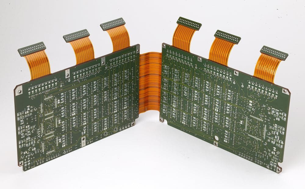
Rigid-flex PCB with polyimide flexible substrate.
Designing materials for a rigid-flex board is a co-engineering process of a system that is mechanically, thermally, and electrically coordinated. All the layers will engage with one another under mechanical stress and at high temperatures.
Flexible Core Materials
The flex section uses industry-standard thermoplastic polyimide (PI) film. Designers often specify adhesiveless polyimide laminates such as DuPont Pyralux AP for high-reliability designs. DuPont Pyralux AP features a glass transition temperature of approximately 220 °C.
When configuring a flex PCB stackup, total thickness is the most critical variable engineers overlook. A smaller composite flex stackup thickness directly ensures a tighter minimum bend radius.
R_min = k × T_composite
The multiplier k depends on application type:
When configuring a flex PCB stackup, total stackup thickness is one of the primary factors that determines the minimum bend radius (Rmin = k × T). According to IPC-2223E, the bend-radius multiplier (k) should be selected based on the exact layer count and application type rather than simplified layer groupings. For static (flex-to-install) applications, IPC-2223E recommends k = 6 for single-layer circuits, k = 12 for double-layer circuits, and higher values for multilayer circuits depending on their construction.
For dynamic (continuous-flex) applications, the recommended thickness multipliers increase significantly to mitigate copper fatigue cracking, with dynamic designs typically restricted to a maximum of 2 layers. Common industry guidelines recommend a multiplier of k = 100 for single-layer circuits, and k = 150 for double-layer circuits. Multilayer constructions should not be used for continuous dynamic flexing. Standard polyimide core thicknesses range from 12.5 to 150 µm, with 12.5 µm and 25 µm cores generally preferred for tight enclosures and dynamic bending because they help achieve smaller minimum bend radii.
Copper foil choice is equally critical. Electrodeposited (ED) copper has a columnar grain structure that cracks under mechanical deflection. Rolled-annealed (RA) copper has a lamellar microstructure that withstands approximately 20–40% elongation without fracturing. RA copper is strongly recommended in all dynamic-flex zones; ED copper is generally suitable for rigid sections and static-flex applications but is not recommended for dynamic bending areas.
1Adhesive vs. Adhesiveless Construction
Adhesive-based cores bond copper to PI via a 12.5–25 µm acrylic layer. Adhesiveless cores cast PI resin directly onto copper via high-vacuum sputtering.
For signal integrity, adhesiveless construction is generally preferred. Acrylic adhesives exhibit $Dk \approx 3.6-3.8$ and a dissipation factor that climbs above ~0.02 at multi-GHz frequencies, increasing dielectric loss and introducing impedance discontinuities. Adhesiveless all-polyimide FCCLs provide a more stable, weave-free dielectric environment with $Dk \approx 3.4$ — and low-loss grades such as DuPont Pyralux AP hold $Df \approx 0.002$ into the GHz range — supporting high-speed, impedance-controlled designs.
Mechanically, acrylic adhesive is a reliability liability: its $Tg$ is only ~100 °C, and its Z-axis CTE is extremely high. During 260 °C lead-free reflow, it generates significant Z-axis expansion via copper barrels, causing barrel cracking and inner-layer separation. Adhesiveless cores eliminate this failure mode.
Design Tip
Use adhesive-less laminates for any design above 5 GHz that requires via reliability through reflow cycles or is rated for dynamic bending.
2Coverlay vs. Solder Mask
Polyimide coverlay is a solid PI film laminated under vacuum and pressure, offering dielectric strength exceeding 5,000 V and reliable performance through repetitive dynamic bending. Its weakness is its loose registration tolerances (±75–100 µm), which require coverlay openings to be expanded by at least 0.1 mm beyond the solder pads.
Flexible LPI solder mask is a photo-defined liquid epoxy with tight registration (±25 µm), ideal for BGA and fine-pitch SMT zones. Its critical flaw is brittleness: it cracks under repeated flexing, exposing copper to corrosion.
Best Practice
Apply coverlay over all bends and dynamic flex regions. Apply LPI solder mask in high-density rigid assembly zones. Position the material transition well away from primary bend zones to avoid stress concentration.
Rigid Flex PCB Design Rules for Rigid Flex Stackup
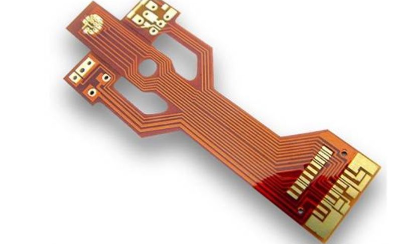
Flexible printed circuit with ENIG gold contacts.
Standard rigid-board DRC rules do not apply to rigid-flex hybrids. The rigid-to-flex interface introduces unique mechanical boundary conditions requiring dedicated rules. Each rule below follows the format:
What it is → why it is necessary → specific values.
Symmetry Rules
All layers, copper weights, and dielectric thicknesses must be mirrored around the stackup's central neutral axis.
The CTE mismatch between FR-4 and polyimide generates massive internal stress during lamination and reflow. An asymmetric stackup causes uneven stress distribution on cooling, producing board warp, bow, and twist that prevent SMT coplanarity and cracked traces.
Match dielectric layer pairs to within ±10% thickness tolerance. Mirror copper weights exactly (e.g., 1/2 oz / 18 µm on all outer flex layers). Neutral axis position:
y_na = Σ(E_i · t_i · y_i) / Σ(E_i · t_i)
Routing in the Bend Zone
Strict geometric rules govern trace orientation and plane treatment in the flex bend region.
Traces shall cross the bend line perpendicularly; any traces running parallel or diagonal to the bend line experience non-uniform tensile and shear stresses, leading to accelerated fatigue failure. Solid copper planes act as rigid hinges that concentrate stress at the transition.
Traces must cross the bend line at 90° using concentric arcs with no sharp corners. Stagger adjacent-layer traces by 12–20 mils to eliminate "I-beam" stiffness. Cross-hatch ground planes at 30–40% coverage (0.2 mm line width, 0.4 mm pitch) and widen traces by +10% to compensate for the resulting 5–16% impedance rise.
Via Placement Restrictions Near the Rigid-Flex Transition Zone
A dedicated keep-out zone shall be maintained for all plated through-holes and vias near the transition line.
Vias are rigid copper stress risers. Near the transition zone, bending concentrates shear stress on the via plating, causing knee fractures and open circuits.
No vias are permitted in the flex bend zone. Minimum keep-out of 50 mils (1.27 mm) from the transition boundary. The industry norm is to use 125 mils (3.175 mm) as the standard. Minimum drill-to-copper spacing: 8 mils (0.20 mm).
| Design Parameter | Minimum | Recommended | Function |
|---|---|---|---|
| Flexible Trace Width | 8 mils (0.20 mm) | 8 mils (0.20 mm) | Minimizes stress cracks |
| Trace-to-Trace Spacing | 5 mils (0.125 mm) | 8 mils (0.20 mm) | Prevents shorts during flexing |
| Via Keep-out from Transition | 50 mils (1.27 mm) | 125 mils (3.175 mm) | Prevents via cracking |
| Coverlay Overlap into Rigid | 40 mils (1.0 mm) | 80 mils (2.0 mm) | Strong lamination bond |
| Stiffener Overlap to Flex Edge | 30 mils (0.76 mm) | 50 mils (1.27 mm) | Eliminates stress concentration |
| Transition Zone Fillet Radius | 1.5 mm | 3.0 mm | Distributes tear forces |
| Copper Shield Coverage | 30% Hatched | 40% Hatched | EMI shielding vs. flexibility |
| Drill-to-Copper Clearance | 6 mils (0.15 mm) | 10 mils (0.25 mm) | Prevents lamination breakout |
From Rigid Flex Stackup to Prototype and Assembly
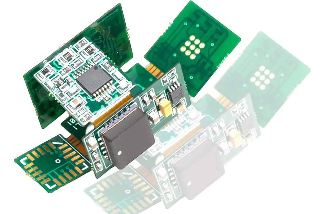
Folded rigid-flex PCBA with SMT components.
Translating a validated stackup into a reliable assembly requires five sequential stages:
-
Document Preparation
Complete engineering package: ODB++ or Gerber databases, a 2D mechanical drawing with transition boundaries, a cross-sectional stackup diagram with layer-level tolerances, and specific material callouts, not generic descriptions.
-
Quote Submission
Highlight the "bikini" coverlay configuration, stiffener placements, and minimum bend radii so that fabricators can accurately estimate panel utilization and lamination cycles.
-
DFM Review
Targets trace-to-edge clearances, via-to-transition compliance, and no-flow prepreg window alignment.
-
Prototype Production
Flex cores are etched and covered first, then low-flow prepregs and rigid caps are cured under high pressure.
-
Issue Analysis
Uses cross-sectional microsectioning, thermal shock cycling, and dynamic bend testing, where required, to validate flex life before full assembly begins.
What to Include in Your Stackup Documentation for Accurate Manufacturer Quoting
Every fabrication drawing must explicitly define: rigid area, flex area, and transition zone boundaries with bend lines and stiffener placements; precise thickness of every layer, full material callouts with manufacturer, grade, and trade name. Selective coverlay overlap distance (40–100 mils / 1.0–2.5 mm) with explicit prohibition of coverlay adhesive in PTH zones; and minimum bend radius, bend angles, cycle life, and static vs. dynamic classification.
DFM Checklist: The 7 Stackup Issues Manufacturers Flag Most Often in Prototypes
1Standard Prepreg Resin Bleed-out at the Transition Boundary
Issue
- Standard high-flow prepregs (1080/7628 glass fabrics) liquefy during secondary lamination and flow onto the flex ribbon. Brittle squeeze-out zones concentrate stress when the flex arm bends, snapping and tearing copper traces.
Solution
Specify high-Tg no-flow or low-flow prepregs (Isola FR406N or Ventec VT-47PP (NF/LF)) with a CNC-routed cutout window matching the rigid boundary.
2Solid Coverlay Acrylic Adhesive in PTH Zones
Issue
- Coverlay and its acrylic adhesive extend continuously through the entire rigid section. Acrylic CTE exceeds 200 ppm/°C. At 260 °C reflow, the acrylic adhesive generates significant Z-axis expansion stress on plated through-hole (PTH) barrels, causing cracking and open circuits.
Solution
Selective "bikini" coverlay terminating 40–100 mils into the rigid section; no PTHs within the overlap zone.
3Vias Placed Inside the Transition Zone Keep-out
Issue
- PTH, blind, or buried vias are placed within the flex bend region or adjacent to the transition line. Mechanical stress concentrates at the transition interface, producing micro-cracks and intermittent electrical failures.
Solution
Enforce a 50-mil (1.27 mm) minimum via keep-out from the transition boundary.
4Asymmetric Lamination and Unbalanced Copper Distribution
Issue
- Flex core offset from center, or mismatched copper weights and dielectric thicknesses on mirrored layer pairs. CTE mismatch causes extreme warp and twist during lamination cooling, preventing SMT coplanarity.
Solution
Mirror all copper weights, core thicknesses, prepregs, and coverlays precisely across the central flex core.
5Vertical Trace Overlap ("I-Beaming") on Multilayer Flex
Issue
- Traces on adjacent flex layers are routed directly on top of each other. Creates I-beam stiffness that prevents bending and causes rapid metal fatigue under minimal flexure.
Solution
Stagger traces horizontally by at least 12–20 mils (0.3–0.5 mm) between adjacent flex layers.
6No Mechanical Stiffeners under Component Assembly Zones
Issue
- Heavy components or connectors are placed on the flex section without a backing stiffener. The flex section bends at pad edges during SMT assembly, causing solder joint fracturing and pad lifting.
Solution
Specify FR-4 (0.2–0.8 mm) or polyimide stiffeners on the reverse side of any flex-mounted components.
7No Pre-baking Specification Before Soldering
Issue
- Sending rigid-flex panels to reflow without a dry-baking procedure. Polyimide and associated adhesives absorb 0.8% to 2.0% moisture. At 260 °C, it flash-vaporizes into steam, causing internal blistering and layer separation.
Solution
Mandate a pre-baking profile of 2–10 hours (depending on design complexity) at 110–120 °C before any thermal assembly process.
The 7 issues above share a common root cause: information gaps between the design team and the manufacturer at the stackup stage. Catching these early before fabrication begins requires close collaboration between layout and manufacturing.
Rigid Flex PCB Cost Breakdown – How Stackup Decisions Drive Your Budget
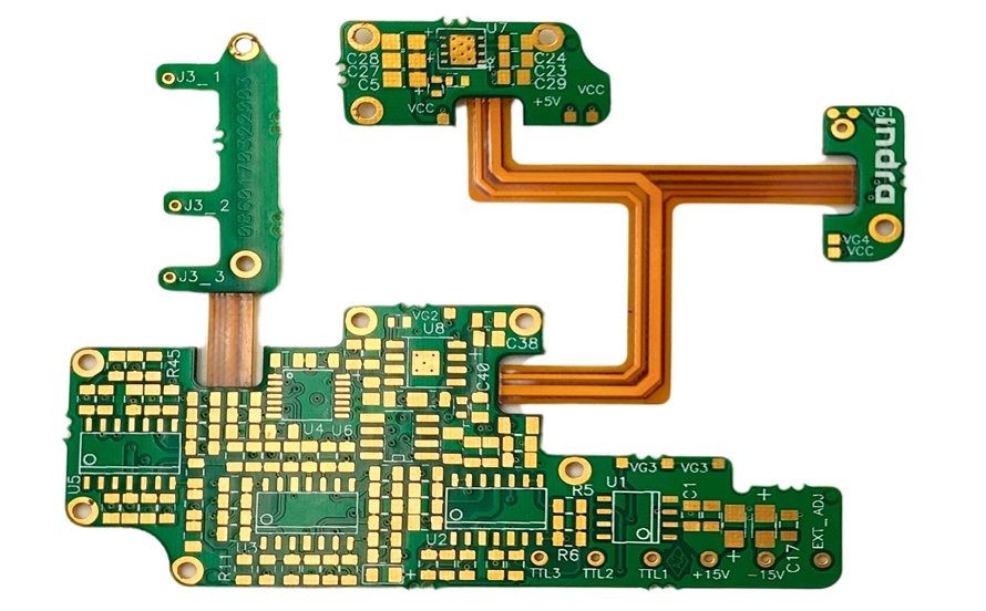
Unpopulated rigid-flex PCB with custom form factor.
Unidentified DFM errors don't just compromise reliability. They force layout rework, duplicate tooling, and complete board re-spins. Understanding how stackup decisions map to cost is the most effective way to prevent those penalties before fabrication begins.
Material Cost Factors
The primary cost driver is the material premium of flexible substrates. High-quality FR-4 costs ~$2 per square foot; high-performance polyimide films like DuPont Pyralux AP range from $6 to $60 per square foot, a 3× to 30× difference before processing. RA copper foil adds a 20–35% premium over ED copper due to multi-step rolling and annealing. Coverlays require selective die-cutting or laser routing to expose rigid assembly areas, a processing step that cannot be eliminated without destroying via reliability.
Layer Count vs. Cost
Cost scales exponentially with layer count. A 2-layer flex PCB costs 1.5–2x more than a single-layer board; each additional layer beyond two escalates fabrication cost by 15–25%. Moving from a 4-layer to a 6-layer rigid-flex stackup typically increases total cost by 20–30%, driven by sequential lamination cycles and compounding misregistration risk that reduces factory yields.
Assembly Cost Considerations
Despite a unit cost ~7x that of an equivalent rigid board and 2–2.5x that of a flex board, rigid-flex eliminates board-to-board connectors, ribbon cables, and manual wire harnesses entirely. The result is lower total system assembly cost, reduced component count, and simplified single-board electrical testing. Assembly tooling costs are higher, custom palletization fixtures are required, and pre-baking must be built into the workflow.
FAQ about Rigid Flex PCB Stackup
Q: How do you prevent trace fractures in dynamic rigid-flex applications?
Route all copper traces perpendicular to the bend line. Do not stack traces directly on top of each other across multiple layers. Staggering the traces avoids the restrictive I-beam effect. Always keep the termination pads away from the transition zone.
Q: Why use cross-hatched reference planes instead of solid copper in the flex area?
Solid copper planes make the flexible region too stiff. This stiffness leads to mechanical fatigue. Cross-hatching provides the necessary electrical shielding for controlled impedance. It also retains the maximum mechanical flexibility of the polyimide substrate.
Q: How do adhesiveless cores improve reliability in rigid-flex stackups?
Standard acrylic adhesives have a high coefficient of thermal expansion. They expand rapidly under heat and stress the plated through-holes. Adhesiveless cores eliminate this unstable adhesive layer entirely. This design prevents via cracking during thermal cycling.
Q: When should you specify FR4 stiffeners versus polyimide stiffeners?
Use FR4 stiffeners to support heavy component placement zones or mechanical connectors. They provide flat, rigid structural reinforcement. Choose thin polyimide stiffeners to increase thickness at Zero Insertion Force (ZIF) connector contact tips.
Q: What is the purpose of a "bookbinder" construction in multilayer flex zones?
Standard stackups use uniform flex layer lengths. This causes the inner layers to buckle when folded. A bookbinder construction progressively steps the length of each flex layer based on its bend radius. This technique prevents inner-layer wrinkling and tension.
Conclusion about Rigid Flex PCB Stackup
A well-designed rigid flex PCB stackup is the foundation of long-term mechanical reliability, stable electrical performance, and efficient manufacturing. By selecting the right materials, maintaining a symmetrical stackup, following bend-zone routing rules, and preparing complete fabrication documentation, you can significantly reduce prototype risks and improve production yield. If you need expert support with rigid-flex stackup planning, PCB layout, or DFM optimization, the JLCPCB PCB Layout team can help turn your design into a manufacturable, reliable product.
Keep Learning
Rigid Flex PCB Stackup Design: The Complete Guide 2026
Key Takeaways Adhesiveless Polyimide Cores: Cores should be made from adhesiveless polyimide laminates to eliminate inner-layer separation and plated through-hole (PTH) barrel cracking caused by the high Z-axis coefficient of thermal expansion (CTE) of acrylic adhesives. Rolled-Annealed Copper: Use rolled-annealed (RA) copper anywhere the board is designed to bend. Unlike electrodeposited (ED) copper, RA copper features a lamellar grain structure that withstands approximately 20–40% elongation without......
5 PCB Board Layout Design Rules for Manufacturing Success
Key Takeaways Rule-driven PCB layout: Define layout rules before placement begins to reduce revision cycles and fabrication risk. Optimized component placement: Group functional blocks, place critical components first, and maintain assembly-friendly spacing for reliable manufacturing. Efficient trace routing: Keep traces short and direct, control width and spacing, and avoid crosstalk and EMI to ensure signal integrity. Design for manufacturability: Follow manufacturer limits, add fiducials and test p......
How to Prepare PCB Drawings for Fabrication Services?
You already know the frustration of sending a PCB design for fabrication and having it come back with an "on-hold" notice. The drawing stage is where the real headaches start. You can have a perfect simulation, but if your documentation doesn't translate to the factory floor, it’s just expensive scrap metal. Creating a high-quality PCB drawing is essentially building a bridge. On one side, you have your theoretical circuit. On the other hand, you have a physical, high-performing product. The transitio......
How to Choose the Best Printed Circuit Board Layout Services
A high-quality schematic is just one part of the challenge in electronic design. After the schematic design, you need to convert that schematic into a functioning printed circuit board (PCB). An incorrect layout of the PCB can degrade a design's performance, causing many issues like electromagnetic interference (EMI), signal integrity (SI) issues, overheating, or, if it gets that far, a board that cannot be manufactured. So how does an engineer, hobbyist, or project manager figure out the market and c......
How to Use IPC Standards to Optimize Your PCB Layout
Designing a PCB is more than just connecting components on a board—it’s about creating a robust, reliable, and manufacturable design that meets industry standards. That’s where IPC standards come in. The IPC standards are among the most widely accepted and important standards for PCB design and manufacturing. Whether you work in electronics design, or manufacturing. IPC standards will influence how a designer creates their board and how they will prepare it for production in different industries. Thes......
PCB Board Layout in Modern Electronic Design
Printed circuit board (PCB) layout is crucial to build current electronic design. Among the multiple components affecting the dependability, efficiency, and performance of an electrical circuit is one of them. Apart from connecting several electrical components, the arrangement improves signal integrity, reduces noise, and controls temperature. The value of PCB board layout, the best design techniques, and the most crucial considerations for PCB layout construction will be discussed in this article. W......