
How to Prepare PCB Drawings for Fabrication Services?
11 min
- What Is PCB Drawing for Fabrication?
- Step 1 – Creating a Printed Circuit Board Drawing from Circuit Requirements
- Step 2 – Converting PCB Design into PCB Layout Design
- Step 3 – Generating PCB Layout Drawing and Manufacturing Files
- Step 4 – Design for Manufacturability (DFM) Checks
- Step 5 – Final Review Before Sending to Fabrication
- Why PCB Design Drawing and PCB Layout Must Work Together?
- FAQ:
You already know the frustration of sending a PCB design for fabrication and having it come back with an "on-hold" notice. The drawing stage is where the real headaches start. You can have a perfect simulation, but if your documentation doesn't translate to the factory floor, it’s just expensive scrap metal.
Creating a high-quality PCB drawing is essentially building a bridge. On one side, you have your theoretical circuit. On the other hand, you have a physical, high-performing product. The transition between the two is where things either work or fall apart. A clean schematic is great, but it doesn't guarantee a manufacturable board.
This guide is about closing the gap and ensuring your design survives the trip to the fabricator.
What Is PCB Drawing for Fabrication?
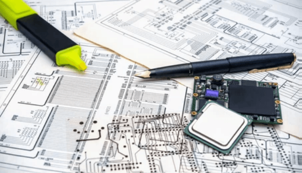
Before anything goes to fabrication, you need to separate three things clearly. In the professional world, a PCB drawing isn't just one file; it’s a full data package. It tells the factory's machines exactly where to etch, drill, and place components with zero room for guessing.
Think of it as three distinct layers of communication:
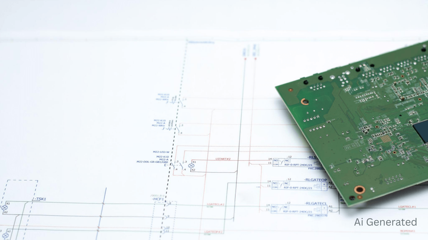
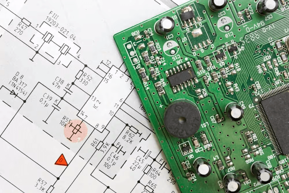
- PCB Design Drawing (The Logic): This is your schematic. It demonstrates the electric connection between things, but is not concerned with physical size or the physical location of a component on the board.
- PCB Layout Design (The Physical): This is the "body." It’s where the schematic logic gets mapped onto a physical board. This is where you decide on trace widths, layer stack-ups, and where that bulky connector is going to go.
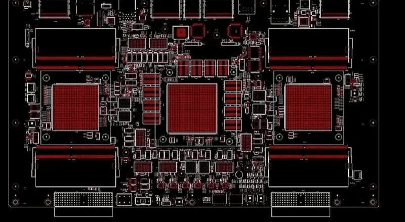
- Fabrication Files (The Instructions): These are the final outputs—your Gerbers and drill files. This is the only thing the machines actually "read."
Accuracy in your PCB drawing is the difference between a high-yield production run and a disaster. I’ve seen designs pass every software check but still fail at fabrication because the pads were just a hair too small for the assembly house's tolerances. It’s a common point of failure that’s easy to miss when you're working fast.
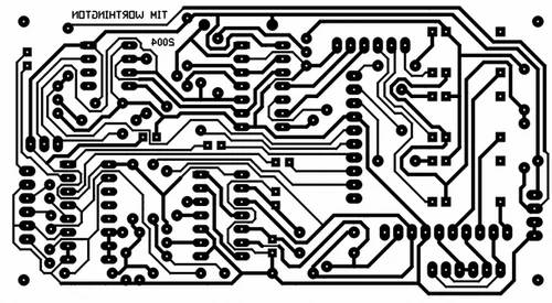
Step 1 – Creating a Printed Circuit Board Drawing from Circuit Requirements
A solid printed circuit board drawing starts long before you open your CAD software. You need a foundation. If you jump straight into routing without a plan, you’ll end up "painting yourself into a corner" where you can’t get your traces to fit.
Defining Functional Blocks
Start by breaking the circuit into blocks. Keep your power management away from your sensitive analog signals. If you mix your high-speed digital lines with your low-level sensor inputs in the PCB design drawing stage, you’re asking for noise issues that are nearly impossible to debug later.
Component Selection: The Real-World Friction
This is where many first-time designs fail. You might find the perfect chip, but if it’s on a 26-week lead time, your project is dead in the water.
- Footprint Accuracy: Never trust a default library 100%. Always double-check the land pattern in my PCB drawing against the manufacturer’s datasheet. A 0.1mm error in a fine-pitch QFN package will ruin your day.
- Thermal Management: When a part will become hot, then you should plan it at this moment. That is, to place thermal vias or copper pours on your PCB design drawing in order to conduct heat off of the silicon.
Common Omissions
Most beginners overlook decoupling. If you don't place your bypass capacitors physically close to the power pins of your ICs, you’ll get voltage ripples that cause "ghost" resets. It is a clichéd error. You must also make sure that your netlist is sound; floating pins are bane to hunt on the real board.
After the schematic has been logically checked, the next hurdle is to convert it into a physical layout that can be produced. That’s where the real work begins.
Step 2 – Converting PCB Design into PCB Layout Design
Here is the engineering rubber to the road. A schematic to a realistic PCB layout design is one of those things to strike a balance between electrical requirements and physical reality.
Why Layout Determines Success
The PCB layout drawing has to respect the factory's limits. For instance, the "Aspect Ratio," which is the board thickness divided by the smallest drill size, is a massive showstopper. If your PCB drawing calls for 0.2mm vias on a thick 2.0mm board, most standard fab houses will kick it back because they can’t reliably plate the inside of that hole.
Placement and Routing Insights
Strategic placement is the heart of a good PCB layout drawing.
- Trace Widths: For general signals, 6–10 mil trace widths are standard. But for power, you need to go wider. It’s better to use a trace width calculator to make sure my copper can handle the current without melting the board.
- Via Sizes: A 0.3mm standard drill is a safe bet for most multi-layer boards. It’s small enough to save space but large enough that every factory can handle it easily.
- Clearance: Stick to a 4–8 mil clearance rule. Going tighter than 4 mils usually moves you into "advanced" manufacturing, which doubles your price.
The Design Rule Check (DRC)
Don't skip the DRC. It’s your safety net. It compares your PCB layout design against the factory's capabilities. It’ll catch things like "acid traps"—those sharp, acute angles in traces that can trap chemicals during etching and eat away your copper.
But that’s only part of the picture. Once the layout looks good, you have to generate the files the factory actually uses.
If you're looking to bridge the gap between a complex circuit and a factory-ready board, you can upload your PCB design to get a manufacturability-optimized layout quote in hours.
Step 3 – Generating PCB Layout Drawing and Manufacturing Files
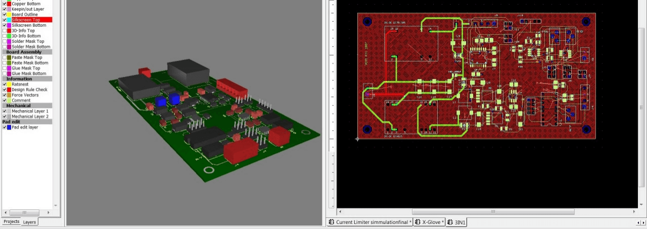
Now we get to the "deliverables." You’ve finished the design, but now you need to speak the factory's language. This is where your PCB layout drawing gets exported into raw data.
The Gerber Standard
Gerbers are the "PDFs" of the PCB world. Your package needs to include:
- Copper Layers: Every single one, from the top to the bottom.
- Solder Mask: This defines where the green (or blue/red) insulation goes.
- Silkscreen: The labels. One pro tip is to make sure your text isn't sitting on top of a solder pad. The factory will just clip it, and you won't be able to read your component labels.
Other Manufacturing File Formats
While Gerbers are the old reliable, high-complexity projects are moving toward "smarter" formats.
- ODB++: This is a much better format because it contains the full intelligence of the PCB drawing—netlists, stack-ups, and component data—all in one zip. It’s harder to mess up.
- IPC-2581: This is the open-standard version of ODB++. If your fab house supports it, use it. It makes the transition from your desk to the factory floor much smoother.
The BOM and Assembly Drawing
Your printed circuit board drawing package isn't done without a Bill of Materials (BOM). I have witnessed numerous projects being put on hold due to the BOM containing the incorrect part number or footprint that was unsuitable for the chip.
Check your reference designators (such as R1, C10) by eye, to ensure that they are the same as what is printed on the silkscreen on the board. After generating the files, you are yet to be fully done. You need a "sanity check" to make sure the board is actually buildable.
Step 4 – Design for Manufacturability (DFM) Checks
Design for Manufacturability (DFM) is concerned with ensuring that your design is not only working on paper, but can be manufactured in large quantities. It is like a difference between a $10 board and a $100 board. Aligning your PCB drawing with factory capabilities is the best way to keep costs down.
Clearance and Annular Rings
You have to account for "drill wander." The machines are precise, yet are not flawless. In case the copper that encircles a hole is too thin (the annular ring), the drill may cut slightly off-center, disconnecting the electricity. This is a common failure point in high-density circuit board drawing projects.
Yield and Cost Factors
Complexity is a price multiplier. If your PCB drawing requires "blind vias" or 10+ layers, your costs will skyrocket. In most professional workflows, we try to stick with through-hole vias and standard 2-to-6 layer stack-ups whenever possible. It keeps the yield high and the headaches low.
This is where the final review comes in. You’ve done the work; now you have to prove it.
Step 5 – Final Review Before Sending to Fabrication
This is the last defense. You have to conduct one last diagnostic test before sending it. Designs that have passed DRC, yet the failure is due to a mere export error.
Schematic-to-Layout Consistency Check
You need to perform a schematic-to-layout consistency check or netlist validation. This is where the software looks at your logic and compares it to your copper. If you accidentally deleted a trace while cleaning up the layout, this is the only way you'll catch it. It’s a vital step that prevents "dead" boards.
Verifying Files for Manufacturing
Download a free Gerber viewer. Don't just trust your CAD software's "export" button. Open the actual Gerber files and look at them.
- Is the board outline on the right layer?
- Are there holes where there should be pads?
- Is the text legible? It only takes ten minutes, and it can save you thousands of dollars in wasted fabrication.
Why PCB Design Drawing and PCB Layout Must Work Together?
The biggest mistake is treating the PCB design drawing and the PCB layout design as separate tasks. They aren't. They are a single, iterative loop. If you find a better way to route a section during layout, you should go back and update your schematic.
The PCB design drawing is the brain, and the layout is the body. Unless they are on track, your project will not be successful.
Each of those stepping out of that initial schematic representation, up to the ultimate netlist verification, is a component of a bigger machine that will guarantee that your board will operate the first time you switch on the switch.
The process of schematic to layout, and DFM checks to final fabrication files is significant to the performance, reliability, and cost efficiency.
Ultimately, PCB layout design does not merely consist of making the prettiest routing. It is the ability to fill the gap between digital theory and mechanical reality.
Get the time to open your final files in a third-party Gerber viewer. It’s the only way to see exactly what the manufacturer sees and catch export glitches that your CAD software might hide. If you want to ensure your next project is 100% production-ready, the right documentation is your best insurance policy.
FAQ:
Q: How do fabrication tolerances impact PCB layout decisions?
Tolerances are the "wiggle room" the factory needs. If you design a PCB drawing with zero tolerance, your boards will fail. As an example, if a trace has a 5 mil thickness and the factory's etching tolerance is ±1 mil, the trace may be only 4 mils thick. That trace will be overheating and breaking in the event that it is already at its current limit.
Q: What file formats do PCB manufacturers prefer besides Gerber?
Most modern houses love ODB++. It’s much more reliable than Gerbers because it automatically includes the layer stack-up and netlist. You don't have to send a separate "ReadMe" file explaining which layer is which. It removes a lot of the human error from the printed circuit board drawing process.
Q: How do you choose the right layer stack-up for a PCB?
It's a trade-off between signal integrity and cost. To the majority of junior engineers, a 4-layer board (Signal-Ground-Power-Signal) is the optimum. It offers a firm ground plane, and your PCB layout will be far more stable and resistant to EMI. Going to 6 or 8 layers will give even better performance, but the cost will increase considerably.
Q: Is auto-routing a good idea for my layout?
Auto-routing is the best, only to a certain extent. Simple, low-speed connections are fine, but anything important (such as power or high-speed data) is still better routed by hand. Most pros will use the auto-router for the "boring" stuff and then spend hours hand-routing the parts that actually matter. Skipping manual routing on critical nets is a mistake you’ll only make once.
Keep Learning
Rigid Flex PCB Stackup Design: The Complete Guide 2026
Key Takeaways Adhesiveless Polyimide Cores: Cores should be made from adhesiveless polyimide laminates to eliminate inner-layer separation and plated through-hole (PTH) barrel cracking caused by the high Z-axis coefficient of thermal expansion (CTE) of acrylic adhesives. Rolled-Annealed Copper: Use rolled-annealed (RA) copper anywhere the board is designed to bend. Unlike electrodeposited (ED) copper, RA copper features a lamellar grain structure that withstands approximately 20–40% elongation without......
5 PCB Board Layout Design Rules for Manufacturing Success
Key Takeaways Rule-driven PCB layout: Define layout rules before placement begins to reduce revision cycles and fabrication risk. Optimized component placement: Group functional blocks, place critical components first, and maintain assembly-friendly spacing for reliable manufacturing. Efficient trace routing: Keep traces short and direct, control width and spacing, and avoid crosstalk and EMI to ensure signal integrity. Design for manufacturability: Follow manufacturer limits, add fiducials and test p......
How to Prepare PCB Drawings for Fabrication Services?
You already know the frustration of sending a PCB design for fabrication and having it come back with an "on-hold" notice. The drawing stage is where the real headaches start. You can have a perfect simulation, but if your documentation doesn't translate to the factory floor, it’s just expensive scrap metal. Creating a high-quality PCB drawing is essentially building a bridge. On one side, you have your theoretical circuit. On the other hand, you have a physical, high-performing product. The transitio......
How to Choose the Best Printed Circuit Board Layout Services
A high-quality schematic is just one part of the challenge in electronic design. After the schematic design, you need to convert that schematic into a functioning printed circuit board (PCB). An incorrect layout of the PCB can degrade a design's performance, causing many issues like electromagnetic interference (EMI), signal integrity (SI) issues, overheating, or, if it gets that far, a board that cannot be manufactured. So how does an engineer, hobbyist, or project manager figure out the market and c......
How to Use IPC Standards to Optimize Your PCB Layout
Designing a PCB is more than just connecting components on a board—it’s about creating a robust, reliable, and manufacturable design that meets industry standards. That’s where IPC standards come in. The IPC standards are among the most widely accepted and important standards for PCB design and manufacturing. Whether you work in electronics design, or manufacturing. IPC standards will influence how a designer creates their board and how they will prepare it for production in different industries. Thes......
PCB Board Layout in Modern Electronic Design
Printed circuit board (PCB) layout is crucial to build current electronic design. Among the multiple components affecting the dependability, efficiency, and performance of an electrical circuit is one of them. Apart from connecting several electrical components, the arrangement improves signal integrity, reduces noise, and controls temperature. The value of PCB board layout, the best design techniques, and the most crucial considerations for PCB layout construction will be discussed in this article. W......