
Stencil Aperture Design: Geometry, Area Ratio & Tips
16 min
- What "Stencil Aperture Design" Really Means
- The Math: Stencil Area Ratio and Aspect Ratio
- Stencil Aperture Geometry – Shape, Walls, and Taper
- Stencil Aperture Reduction Techniques When and Why to Shrink Stencils
- Fine-Pitch Stencil Aperture Design - The Rules Tighten
- Stencil Aperture Design and the Defects Each Rule Prevents
- Why Manufacturing Quality is as Important as Design
- FAQs on Stencil Aperture Design
Key Takeaways
Stencil aperture design controls paste volume, deposit shape, and print registration — it's the key controllable variable in SMT print quality.
IPC-7525B rules are non-negotiable: stencil area ratio ≥ 0.66 and stencil aspect ratio ≥ 1.5.
Aperture geometry is component-dependent: 1:1 with pad for BGA, window-pane splits for QFN/BGA thermal pads, home-plate shapes for 0201/01005 chips, and modest reductions for fine-pitch QFP.
Aperture reductions intentionally decrease the opening relative to the pad to avoid bridging, tombstoning, solder beading, and voiding.
Common print defects such as bridging, insufficient solder, tombstoning, and voiding often trace back to aperture design rules that were not properly followed.
Manufacturing precision matters as much as aperture math — premium stencil services cut to ±0.003 mm, apply engineering review with both default optimization and 1:1 paths, and offer surface treatments for fine-pitch designs.
Each SMT stencil is just a thin sheet of stainless steel with hundreds, sometimes thousands, of laser-cut openings. The steel itself doesn't do anything – it's the openings, the apertures, that determine if solder paste lands on the pad in the right shape and volume for a clean reflow. Industry analyses consistently attribute 60–70% of SMT defects to the solder paste printing process, with many of these issues originating from one upstream decision: stencil aperture design.
This article is a technical reference for the engineer who actually specifies the apertures – PCB designers, SMT process engineers, EMS technicians, and hardware teams that build their own boards. It explains the calculations (area ratio and aspect ratio), the shapes and features (shape, wall taper, wall surface, and alignment), the ways to improve designs (reductions for BGA, QFN, and 0201/01005 components), fine-pitch stencil aperture design for 0.5 mm pitch and below, and how each guideline relates to a specific problem it helps avoid.
Note
This article focuses specifically on stencil aperture design. For broader SMT stencil design topics—including solder paste selection, stencil thickness, frame selection, and printing parameters—refer to JLCPCB's SMT Stencil Design Tips for Improving Solder Paste Deposition. For recommended aperture dimensions, reductions, and component-specific opening standards, see the JLCPCB's Opening Process Standard for Stencils.
What "Stencil Aperture Design" Really Means
The Stencil's Working Surface is the Aperture
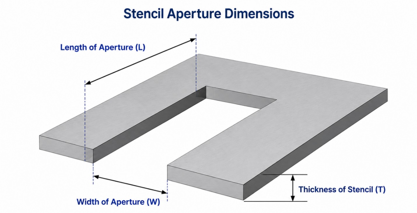
The structural sheet serves as the stencil, and the work is done through the apertures. Aperture size, shape, wall geometry (taper), and positioning in relation to the pad (registration) are the four design variables that are independent of each other. If you get all four right, the paste deposits will be in the right places and volumes.
Why Stencil Aperture Design Is a Discipline, Not A Default
Many designers allow the aperture layer to auto-generate at a 1:1 ratio from the paste/pad layer and do not review it afterwards. That default is fine for about 70% of the components on a typical board — standard 0603/0805 passives and common SOIC and QFP packages. The remaining 30% consists of QFN and BGA thermal pads, 0201/01005 chips, fine-pitch leads, and RF shield frames, all of which require a specific aperture decision rather than the default. This article focuses on the 30% of cases where the default design fails, necessitating a specific design choice.
The Math: Stencil Area Ratio and Aspect Ratio
Stencil Area Ratio Explained (With Formula)
Quick Formula
Area Ratio = area of aperture opening / area of aperture wall
According to IPC-7525B, the figure that is considered acceptable is 0.66 or above. Paste starts to cling to the walls of the aperture rather than being transferred neatly to the pad below that point. No matter the type of paste, whether it has been stencil-treated or not, the print yield below approximately 0.50 is uncertain.
Aspect Ratio and When it Turns into the Limiting Constraint
Quick Formula
Aspect Ratio = opening width / stencil thickness; Target: ≥ 1.5
For square or near-square apertures, stencil area ratio is typically the limiting factor. For narrow rectangular apertures, typical of QFP and QFN leads, aspect ratio becomes the binding constraint.
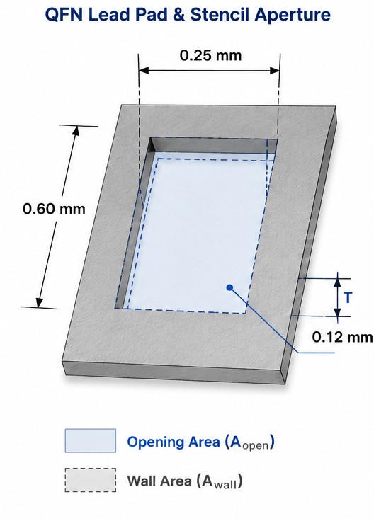
0.4 mm Pitch QFN on a 0.12 mm Stencil – Worked Example
Take a QFN lead pad, about 0.25 × 0.6 mm, on a 0.12 mm stencil.
- Aperture wall area = 2 × (0.25 + 0.6) × 0.12 = 0.204 mm²
- Aperture opening area = 0.25 × 0.6 = 0.15 mm²
- Area ratio = 0.15 ÷ 0.204 ≈ 0.735 — safely above the 0.66 floor
Enhancement of paste release is achieved by reducing the stencil thickness from 0.12 mm to 0.10 mm to further increase the area ratio to about 0.882.
Stencil Aperture Geometry – Shape, Walls, and Taper
The basic rule is that the aperture shape generally follows the pad shape. However, the aperture shape is not always an exact copy of the pad. It may be intentionally modified—for example, using home-plate, reduced, or window-pane designs—to control solder paste volume and prevent defects such as tombstoning, bridging, solder beading, and voiding. These aperture reduction techniques are discussed in the following section.
A laser-cut aperture wall is not perfectly smooth – it has micro-ridges from the cutting process that can trap and retain paste. Electropolishing takes away the ridges and gives the wall a near mirror finish. Nano-coating takes it one step further with a hydrophobic layer on top of the polished surface.
Aperture Registration to Pad
But none of that matters if the aperture doesn't land where it's meant to. Industrial SMT printers are accurate to about ±5 µm, and manual or cheap prototyping setups are often ±50 µm or worse. A perfectly designed aperture that's misregistered by tens of microns will still produce misplaced, smeared, or partial deposits — a reminder that aperture design and print-process control are two separate disciplines that both have to work.
Stencil Aperture Reduction Techniques When and Why to Shrink Stencils
Why Decrease an Aperture Below Pad Size?
The maximum paste volume is achieved with a 1:1 aperture-to-pad ratio and sounds great until it causes a defect. A 1:1 aperture can cause the following primary failure modes:
Failure Modes of 1:1 Aperture
- Bridging – adjacent pads are joined during reflow.
- Tombstoning – chip lifted on one side due to unbalanced surface tension.
- Solder beading – excess paste squeezed out from under the body of the chip during placement.
- Voiding – large solid paste deposit trapping gas under a BGA/QFN thermal pad.
1Home-Plate Reduction for 0201 and 01005 Chips
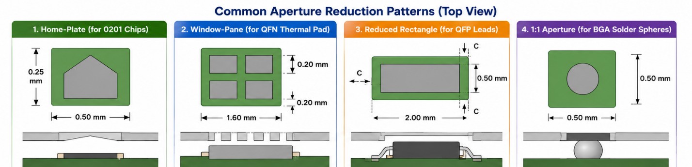
For very small chip components, the aperture takes the shape of a pentagonal "home plate," with the point facing the body of the component. This reduces the amount of paste directly beneath the chip so that the surface tension forces on the two end pads during reflow are balanced and the part does not tombstone. A typical reduction in pad area is 5-10%.
2Standard Aperture Dimensions (Industry Reference) for Chip Components
Most stencil suppliers will by default apply some sort of stencil aperture reduction on chip components rather than cutting a pure 1:1 opening.
3Anti-Solder-Bead Reduction for 0805 and Larger Passives
Solder beading occurs when a chip is placed and squeezes excess paste out from under it, and the paste reflows into a small bead next to the component. This is common with 0805 and larger passives, where the pad area creates more paste than the joint actually requires. The solution is to reduce the aperture on the side of the pad that faces the component body, ensuring that the paste deposit is slightly inset and that excess paste is not pushed out during placement. For passives of 0805 and larger (excluding diodes), JLCPCB defaults to this reduction, but customers can request a 1:1 aperture explicitly when ordering.
4Window-Pane Reduction for QFN/BGA Thermal Pads
Instead of one large opening for a single large thermal pad under a QFN or BGA, it is cut into 4, 6, or 9 smaller apertures separated by narrow stencil "bridges." The spaces between apertures allow trapped gas to escape during reflow. Typical paste coverage for a window-pane split is 60% to 75% of the original pad area.
BGA balls already have their own solder volume. So, the paste deposit job is different than a passive's. It is mainly for wetting, not for primary joint volume. The BGA stencil aperture should be 1:1 with the pad, or very close. Going below around 90% risks starving the joint of paste needed for a good connection.
Fine-Pitch Stencil Aperture Design - The Rules Tighten
What Does Fine Pitch Mean?
Anything at a 0.5 mm pitch and below is considered fine pitch: 0.4 mm BGA, 0.4 mm QFN, 0.5 mm QFP, and 0201 / 01005 chips. At these pitches, the area-ratio margin above the 0.66 floor rapidly shrinks, and aperture dimensional tolerance that is irrelevant on an 0805 pad becomes the difference between a good joint and a defect.
What is Different in 0.4 mm BGA Stencil Aperture Design
BGA pads at a 0.4 mm pitch are around 0.25 mm diameter - small enough that stencil thickness must come down to something like 0.10-0.12 mm just to maintain an acceptable area ratio. BGA stencil aperture should be 1:1 with the pad or a modest 5-10% reduction if voiding is a concern.
Why 0201/01005 Aperture Design Is Unique
These chips are so small that a perfect 1:1 aperture deposits more paste than the joint needs, with excess sitting directly under the component body.
Fine-Pitch Lead Pitch Dependent Aperture Width Standards
JLCPCB publishes some specific aperture width standards by lead pitch, which are a good practical starting reference for fine-pitch QFP, QFN and alike packages.
When to Use a Step Stencil for Mixed Fine + Standard Pitch
A board with a 0.4 mm BGA near a connector or large RF shield needs very different paste volumes in different zones – the fine pitch stencil aperture area needs a thin stencil for area ratio, but the large connector needs a thicker one for enough volume. A step stencil, cut with regions of different thickness on the same sheet, solves that conflict. It does not force a single thickness compromise over the entire board.
Stencil Aperture Design and the Defects Each Rule Prevents
Bridging — Aperture Too Large or Too Close
Cause: An excessive aperture-to-pad ratio, leaving a 1:1 aperture on fine-pitch leads when reduction is needed, insufficient spacing between adjacent apertures or pads, poor stencil registration, or paste smearing during printing can allow excess solder paste to connect neighboring pads during reflow.
Aperture-Design Fix: Reduce the length of the aperture by 5-10%; recheck aspect ratio after.
Insufficient Solder — Area Ratio Too Low
Reason: The aperture is too small in relation to the thickness of the stencil.
Fix: Increase opening, decrease stencil thickness, or both, as long as paste volume is adequate elsewhere on the board.
Tombstoning — Asymmetric Paste Volume
Cause: Equal-sized apertures on both pads, but thermal mass not equal at the two ends of the component during reflow.
Voiding — Gas Trapped Under a Solid Paste Deposit
Fix: Replace a single large aperture with a window-pane split (4, 6, or 9 smaller openings) to provide escape paths for trapped gas during reflow.
Solder Balls — Misaligned or Smudged Paste
Cause: Paste lands outside the pad and reflows into free-standing spheres.
Fix: A tighter aperture for pad registration and verifying the underside of the stencil is clean between prints – a process check, not just a design one.
Why Manufacturing Quality is as Important as Design
A Perfect Aperture Design Needs a Precise Cut
An aperture specified at 0.250 mm but cut to 0.260 mm is no longer the aperture that was designed. At fine pitch stencil aperture, a cutting tolerance looser than about ±0.01 mm changes paste volume by a measurable, defect-relevant amount. At that point, stencil supplier selection is no longer a procurement detail. It is a yield variable.
Surface Treatments to Increase Aperture Design Tolerance
Electropolishing smoothes the roughness of laser-cut walls, typically extending the workable area-ratio floor down to ~0.60 from the IPC baseline of 0.66. Combined with nano-coating, the practical floor can go even lower, to around 0.55, for suitably matched paste types. Neither treatment is a substitute for good aperture design — they both only increase the margin of error therearound.
How Aperture Optimization Works at JLCPCB — Engineering Suggestions, Not Automatic Edits
When you upload a Gerber file to JLCPCB, it's reviewed for engineering before production begins. In that audit, JLCPCB engineers look at the paste layer and, by default, apply the company's published aperture standards for known component types—the chip-component reductions, anti-solder-bead reductions, fine-pitch QFP widths, and thermal-pad bridge patterns described earlier in this article.
-
Automatic optimization applied
JLCPCB applies its published aperture standards when preparing the production file that drives the laser cutter; the customer's uploaded Gerber file itself is not modified. Customers who want this default do not need to take any action.
-
Exact aperture as designed
If the customer wants their aperture design cut exactly as drawn, without any optimization or reduction, they can leave a remark at checkout requesting 1:1 production from the paste layer, and JLCPCB will cut the stencil to match the uploaded paste layer precisely.
In both cases, the JLCPCB engineers do not edit the customer's original source design files. Any optimization is done only in the production file generated from the Gerber data. The default is most useful for customers that haven't computed reductions independently for each chip component or fine-pitch lead - it provides a known-good starting point. We have a 1:1 option for customers who have already done their aperture engineering (fine-pitch, RF, or specialty designs) and want to preserve their exact intent.
Why Do Engineers Order Aperture Optimized Stencils From JLCPCB?
The combination that ensures effective design decisions for apertures actually holds up in production is laser cutting precision around ±0.003 mm, well beyond what most aperture specs require, paired with engineering review on every order and support for both the optimization and 1:1 paths described above. Electropolishing and nano-coating are standard process options and not special requests. Stencils are cut from 304 HTA stainless steel and retain their stencil aperture geometry through repeated cleaning cycles. Prototyping makes it practical to validate and refine stencil aperture designs through multiple design iterations before committing to a final specification, helping improve print quality and reflow performance. As an ordering advantage, JLCPCB offers custom SMT stencils starting at $3, a minimum order quantity (MOQ) of 1, and production in as little as 12 hours, making rapid design iteration both convenient and cost-effective.
What This Article Won't Cover
This article stays deliberately narrow — stencil aperture-level design parameters only: area ratio and aspect ratio math, aperture geometry, reduction techniques, and the defects each one prevents. Broader stencil design topics — paste selection, squeegee pressure and speed, print gap, frame type, and general print-process troubleshooting — are covered in JLCPCB's companion guide, SMT Stencil Design Tips for Improving Solder Paste Deposition.
FAQs on Stencil Aperture Design
Q: Is a better print always associated with a high area ratio?
Not necessarily. A higher area ratio improves paste-release reliability by allowing solder paste to transfer more consistently from the stencil to the pad. However, it does not automatically guarantee better print quality because increasing the area ratio often requires either enlarging the aperture or reducing the stencil thickness, both of which affect the deposited paste volume. A successful stencil design therefore balances area ratio, paste volume, and stencil thickness to achieve reliable paste transfer without introducing defects.
Q: Can I use the same stencil thickness for a board with a 0.4mm BGA and standard 0805 passives?
Often not without a price. Choose a thickness for the ratio of fine pitch stencil aperture areas, and you won't get enough paste on the larger pads; choose a thickness for standard components, and you'll fail the ratio of the fine pitch parts.
Q: What is the real effect of aperture wall taper on yield?
Taper by itself is mostly about consistency at the edges, i.e., boards with tight aspect ratios or long print dwell times will see the most significant gains from adding taper and smoothing walls, while boards with ample aspect ratios all around might show little real difference.
Q: What's the quickest way to confirm that my aperture design will bridge or be void prior to sending files for production?
Determine the area ratio and aspect ratio for each distinct aperture family on the board, not just the tightest-pitch component, and verify that they meet the recommended 0.66 and 1.5 thresholds. To reduce the risk of bridging, also check aperture spacing, pad registration, and aperture reductions on fine-pitch components to ensure solder paste does not spread between adjacent pads. For thermal pads on QFN and BGA packages, verify that the aperture uses a segmented window-pane pattern rather than a single large opening to promote gas escape during reflow and minimize voiding. Evaluating these design features before fabrication helps identify potential bridging and voiding issues before the stencil is manufactured.
Conclusion: Stencil Aperture Design Decides Print Quality, Not Steel Quality
For every stencil aperture design on the board, the absolute minimum requirements are a stencil area ratio of 0.66 and an aspect ratio of 1.5. For example, in the case of BGA, the stencil aperture geometry is 1:1. In the case of thermal pads, they are windowpanes, and in the case of the tiniest chips, they are home plates. Furthermore, stencil aperture reduction techniques are not available as a general precaution but rather for specific identified problems. These are the most important factors affecting SMT print quality, even more than the steel used for cutting. They are not afterthoughts or extras on top of a "good enough" stencil.
Keep Learning
Stencil Aperture Design: Geometry, Area Ratio & Tips
Key Takeaways Stencil aperture design controls paste volume, deposit shape, and print registration — it's the key controllable variable in SMT print quality. IPC-7525B rules are non-negotiable: stencil area ratio ≥ 0.66 and stencil aspect ratio ≥ 1.5. Aperture geometry is component-dependent: 1:1 with pad for BGA, window-pane splits for QFN/BGA thermal pads, home-plate shapes for 0201/01005 chips, and modest reductions for fine-pitch QFP. Aperture reductions intentionally decrease the opening relative......
Solder Paste Stencil Defects: Causes and Fixes for Higher SMT Yield
Usually, the circuit board stencil is responsible for roughly 60% to 70% of all SMT defects. That number surprises people. It shouldn't. The stencil controls paste volume, deposit geometry, and positional accuracy all at once. When it gets wrong, everything downstream pays for it. The shift in thinking that separates good engineers from great ones is simple: stop seeing the PCB stencil as a metal sheet with holes in it. It is a precision fluid delivery system. Every aperture wall, every micron of foil......
SMD Glue & Red Glue: A PCB Assembly Application Guide 2026
The reality of modern PCB assembly is that "mixed-technology" is still very much the norm. When a board hits the wave soldering machine, bottom-side SMD components face a high-velocity river of molten metal. Without a solid mechanical bond, they’ll simply wash away into the solder pot. That’s where the precision application of SMD glue becomes the difference between a successful run and a bin full of scrap. Quick Answer: How to Apply SMD Glue in SMT If you need to configure your SMT stencil for adhesi......
SMT Stencil Cleaning Guide: Process, Frequency, and Tips
Key Takeaways about SMT Stencil Cleaning SMT stencil cleaning removes solder paste residue from aperture walls and the stencil underside, keeping paste transfer efficiency between 80% and 100%. Industry analysis attributes over 60% of SMT defects to the paste-print step — most of which trace back to a stencil cleaning lapse. Two stages matter: under-screen cleaning (between cycles, typically every 5–10 prints) and off-line cleaning (after production completes). IPA handles standard flux residue; dedic......
The Essential Guide to SMT Stencils in PCB Assembly
Introduction In the dynamic world of electronics manufacturing, Surface Mount Technology (SMT) plays a crucial role in achieving efficiency and precision in printed circuit board (PCB) assembly. Central to the SMT process is the SMT stencil, an indispensable tool for the accurate application of solder paste. This ensures solid electrical connections between components and PCBs. This guide delves into the specifics of SMT stencils, examining their types, materials, manufacturing methods, advantages, ch......
Nano-Coatings in PCB Manufacturing: How They Outperform Traditional Stencils
Nano coating is a thin hydrophobic (water repellent) and oleophobic (oil repellent) treatment used on the undersides and edges of solder paste stencils. With this the surface becomes non-stick which reduces the number of cleaning cycles required for the solder paste printing process. Upon application, the less than 5 nanometer coating bonds with the stencil foil at the microscopic level, which does not change the size and shape of the stencil. Nano coating is an industry proven process which shows imm......