
Top 5 Circuit Board Stencil Mistakes & How to Fix Them for Higher SMT Yield
11 min
- Quick Answer: Circuit Board Stencil Mistakes to Avoid
- What Is a Solder Paste Stencil?
- Mistake #1: Guessing Your Solder Paste Stencil Thickness
- Mistake #2: Using 1:1 Apertures on a Solder Paste Stencil
- Mistake #3: Skipping Polishing on Fine-Pitch Stencils
- Mistake #4: Forgetting Fiducials on a Solder Paste Stencil
- Mistake #5: Using Incompatible Glue on a Framed Stencil
- How to Avoid Stencil Mistakes (Decision Checklist)
- How to Order a Flawless Solder Paste Stencil
- Frequently Asked Questions about Circuit Board Stencil:
Usually, the circuit board stencil is responsible for roughly 60% to 70% of all SMT defects. That number surprises people. It shouldn't. The stencil controls paste volume, deposit geometry, and positional accuracy all at once. When it gets wrong, everything downstream pays for it.
The shift in thinking that separates good engineers from great ones is simple: stop seeing the PCB stencil as a metal sheet with holes in it. It is a precision fluid delivery system. Every aperture wall, every micron of foil thickness, every fiducial location is an engineering decision with a direct consequence on yield.
Quick Answer: Circuit Board Stencil Mistakes to Avoid
If you want to ensure high first-pass yield in your SMT assembly, ensure you are not making these five common stencil errors:
-
Guessing Stencil Thickness: Failing to match the foil thickness to the tightest component pitch on the board.
-
Using 1:1 Aperture Ratios: Exporting apertures identical to pad sizes, leading to tombstoning and heavy voiding.
-
Skipping Advanced Surface Finishes: Ignoring electropolishing or nano-coating on fine-pitch designs.
-
Missing Fiducial Marks: Forgetting to include globally asymmetrical optical alignment targets.
-
Using Incompatible Frame Adhesives: Utilizing standard epoxies that degrade during ultrasonic cleaning.
To help you optimize your process, we have prepared this ultimate guide detailing these top 5 mistakes and exactly how to fix them.
What Is a Solder Paste Stencil?
A solder paste stencil is a precision laser-cut stainless steel foil used as a physical template to deposit solder paste with exact volumetric control onto bare PCB pads. The critical word there is volumetric.
The stencil is not a 2D masking tool. It is a 3D engineering instrument where foil thickness and aperture geometry together determine how much paste lands on each pad. Get either dimension wrong, and your defect rate reflects it immediately.
There are two formats to choose from:
-
Frameless (Foil-Only)
This is the kind of stencil that doesn’t come with a supporting frame. It’s a bare laser-cut sheet. These are typically lightweight as well as affordable. For hand printing or rapid prototyping, these work best for their setup time and cost implications.
-
Framed:
The stainless steel foil is permanently tensioned across a rigid cast-aluminum frame using a mesh border and industrial epoxy. This format is required for automated SMT printers in mass production — the frame maintains foil flatness and consistent gasketing under repeated high-speed squeegee strokes.
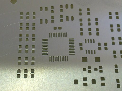
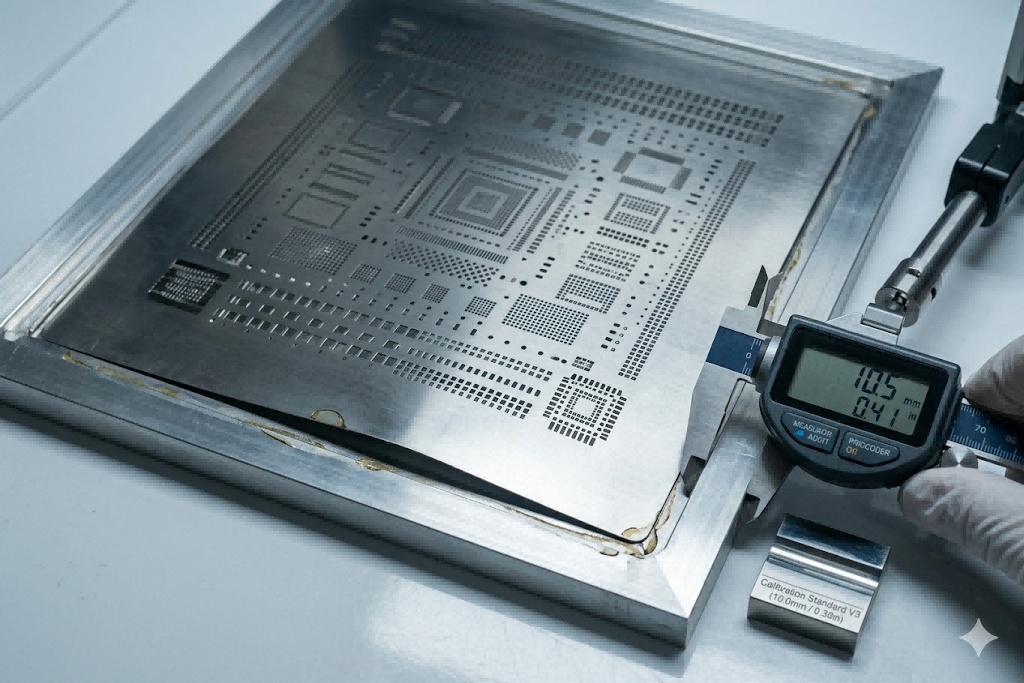
Mistake #1: Guessing Your Solder Paste Stencil Thickness
The most common mistake engineers make is treating thickness as a fixed preference—for example, picking 0.15mm just because it worked on the last board.
If your SMT stencil thickness is too high for a fine-pitch component, you deposit excess paste volume, which becomes bridging during reflow. Too thin, and joints come out lean, mechanically weak, and prone to failure under thermal cycling. The fix is matching the thickness to the tightest component pitch on the board, not the average pitch.
-
0.10mm: For 0.4mm pitch ICs/BGAs and 0.5mm pitch BGAs.
-
0.12mm: For 0402 components, 0.5mm pitch ICs, and 0.65mm pitch BGAs.
-
0.15mm: For larger components (ICs ≥ 0.65mm pitch and BGAs ≥ 0.8mm pitch).
Impact on SMT Yield:
Guessing stencil thickness accounts for up to 60% of volume-related SMT defects, frequently driving bridging reject rates above 15% on fine-pitch boards.
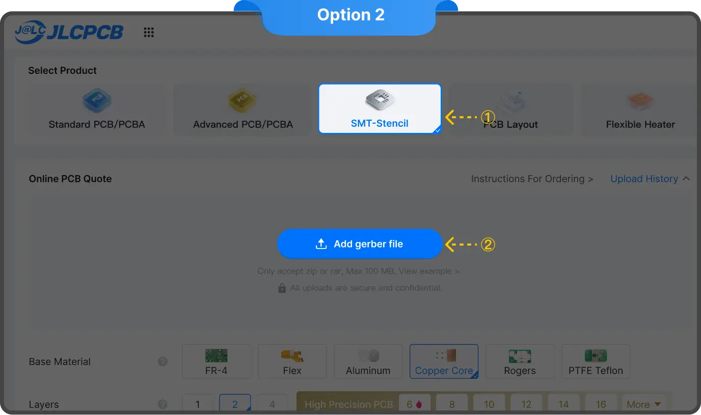
When you custom the stencils, to make things even easier, the "Select by JLCPCB" option eliminates this calculation entirely. It's a feature in the online ordering process, where the customer doesn't need to go through complex thickness calculations. The in-house engineering team gets it done for them.
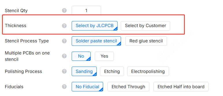
However, if you want to go with your own thickness requirements, you get the manual option too.
Mistake #2: Using 1:1 Apertures on a Solder Paste Stencil
Exporting apertures at an exact 1:1 ratio with the copper pads feels intuitive. The pad is this size, so the aperture should match. In practice, it causes two distinct failure modes that are expensive to diagnose after the fact.
-
On passive components like 0805 or 1206 resistors, excess paste from full-size apertures becomes a problem. It creates unequal surface tension during reflow. One end of the component wets before the other, and the imbalance pulls it upright. The result is tombstoning. The joint is destroyed before the board leaves the oven.
-
On large thermal pads above 4×4mm, a solid 1:1 aperture deposits a continuous block of paste that traps outgassing flux during reflow. The result is massive voiding under the component, which kills thermal performance in power devices and often fails reliability testing outright.
Impact on SMT Yield:
Using 1:1 apertures on passive components can increase tombstoning defect rates by over 12%, and cause unacceptable voiding (>30%) under QFN/BGA thermal pads.
The fixes are well-established. For passive components prone to tombstoning, use home-plate, U-shape, or chamfered aperture geometries. These reduce paste volume at the pad edges, balancing the wetting force during reflow.
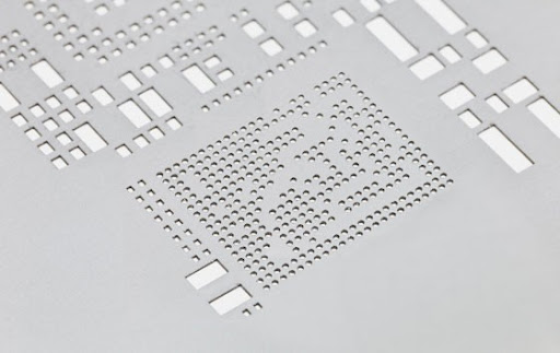
For large thermal pads, apply a windowpane cross-hatch pattern with a minimum gap of 0.3mm, creating a grid that allows flux gases to escape cleanly.
Via tenting matters here, too. Apertures must avoid any PCB vias or plated through-holes within the pad boundary. Paste that enters a via hole will not deposit on the pad, and cleaning it out wastes line time.
JLCPCB's CAM team provides optimization suggestions based on customer designs before laser cutting. So the stencil that arrives is already optimized for high first-pass yield.
Learn more about JLCPCB's opening process standard for stencils.
Mistake #3: Skipping Polishing on Fine-Pitch Stencils
A raw laser-cut foil has a problem that is invisible to the naked eye but shows up immediately in paste transfer data. There are often microscopic thermal burrs along the inner aperture walls that you get from the laser cutting process.
These create friction during snap-off, which ends up gripping the paste instead of releasing it cleanly. As a result, you end up with clogged apertures, missing deposits, and yield loss that looks like a printer calibration issue. You only get to know about this after examining the stencil walls properly.
For standard pitches above 0.5mm, this is manageable. For anything finer, like 01005 components, sub-0.4mm BGAs raw walls make repeatable printing nearly impossible.
Impact on SMT Yield:
Rough aperture walls can reduce paste transfer efficiency by 15-25%, making repeatable printing on 01005 components or sub-0.4mm BGAs virtually impossible.
Electropolishing resolves this by using an anodic dissolution process to smooth the laser scallops to a mirror-like finish. Paste releases cleanly and consistently, and your SPI volume data tightens noticeably. That’s what JLCPCB does to avoid this problem.
For the most demanding applications, JLCPCB's Nano-Coating goes further. It increases steel surface hardness, ensures reliable paste release on ultra-fine apertures, along with extending the under-wipe interval to up to 30 print cycles. This results in a meaningful throughput gain on any volume line.
Mistake #4: Forgetting Fiducials on a Solder Paste Stencil
This one stops production lines cold. Fiducial marks are the visual reference points that automated SMT printer cameras use to align the stencil to the PCB. Without them, the machine is printing blind, and it knows it. Most modern printers will halt and throw an alignment error rather than proceed with a misregistered print.
Even a 50 μm misalignment on a 0.5mm pitch component places paste on the solder mask rather than on the pad. That deposit will not wet properly during reflow. You get balling, poor joint formation, and bridging on adjacent leads. All from a missing fiducial in the Gerber export.
Impact on SMT Yield:
Missing fiducials cause 100% line stoppage on automated equipment, or massive misregistration failures resulting in batch scrapping.
The standard is a minimum of three globally asymmetrical fiducials. Asymmetrical placement prevents the vision system from accepting a 180° rotated stencil as a valid alignment, a subtle but important detail.
And the best part is that JLCPCB offers three fiducial options to match your printer type: No Fiducial, Etched Through, and Etched Half-Into-Board.

Mistake #5: Using Incompatible Glue on a Framed Stencil
Framed stencils are mandatory for automated production lines. But there is a failure mode that rarely gets discussed until it happens: putting a standard framed stencil through an industrial ultrasonic cleaner.
Ultrasonic cleaning uses intense vibration and hot chemical solvents to strip flux residue. Standard yellow frame epoxy was not engineered for that environment. Under repeated exposure, the adhesive degrades, the mesh sags, and the foil loses tension.
Oil-canning follows the foil flexes under squeegee pressure, the gasket seal breaks down, and print quality deteriorates across the entire board. By the time the root cause is identified, a production run has been compromised.
Impact on SMT Yield:
Frame adhesive degradation causes loss of foil tension, leading to unpredictable, inconsistent paste volumes and smearing across the entire production batch.
The fix is specifying the right adhesive from the start. JLCPCB uses an imported ultrasonic-resistant AB epoxy to bond the foil mesh to the aluminum frame. It withstands extreme temperatures, harsh cleaning chemicals, and sustained ultrasonic vibration. It’s built for the cleaning environments that production stencils actually face.
How to Avoid Stencil Mistakes (Decision Checklist)
Before sending your files to manufacturing, run through this quick checklist:
-
Match Thickness:
Did I select thickness based on the smallest component pitch?
-
Optimize Apertures:
Are my passive and thermal pad apertures reduced/cross-hatched (not 1:1)?
-
Select Finish:
Have I specified electropolishing or nano-coating for sub-0.5mm pitches?
-
Verify Fiducials:
Are there at least 3 asymmetrical fiducials included in the design?
-
Check Frame Glue:
If using automated cleaning, is the frame bonded with ultrasonic-resistant AB glue?
How to Order a Flawless Solder Paste Stencil
There's no guessing in perfect SMT assembly. It’s a science that demands thorough planning and execution. All of that starts with the stencil. The five mistakes above are entirely avoidable when the tooling is specified correctly from the beginning.
JLCPCB's stencil ordering workflow is built around eliminating these failure points.
Here's how it works:
-
Upload your Gerbers, let the "Select by JLCPCB" system assign the correct thickness
-
Review the automatically applied aperture modifications
-
Select premium upgrades: Nano-coating or AB glue frame bonding.
-
Offers various fiducial types in under five minutes.
With all these preventive measures, you get custom JLCPCB stencils starting at $3 USD with no minimum order quantity and a build time as fast as 12 hours.
Choose from Framed/Frameless, Electropolishing, Nano-coating, Step-Stencils, SMD Glue Stencil and more. Starting at $3. No MOQ. 12-Hour production.
Get $11 Coupon Now >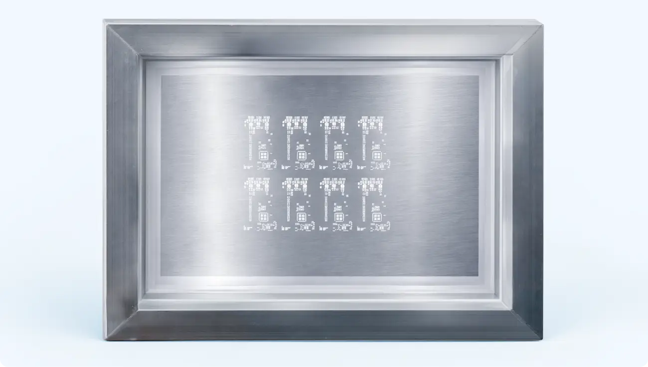
Frequently Asked Questions about Circuit Board Stencil:
How many prints can I get from a stainless steel stencil?
A well-maintained stainless steel stencil typically handles 50,000 to 250,000 print cycles. Inspect aperture edges under magnification every 10,000 cycles on high-volume lines and retire based on measured transfer efficiency rather than visual wear alone.
Do I really need nano-coating for standard assembly?
For pitches above 0.5mm, electropolishing is sufficient. Nano-coating earns its cost at sub-0.4mm pitch and for 0201 or 01005 components, where paste release consistency directly determines yield.
What is the difference between a framed and a frameless PCB stencil?
A framed stencil is permanently bonded to an aluminum frame required for automated SMT printers in production. A frameless foil-only stencil mounts to a reusable universal holder and is more cost-effective for prototyping or low-volume runs.
How does squeegee pressure affect solder paste stencil performance?
Too much pressure forces paste under the foil and drives bridging. Too little pressure leaves residual paste on the surface instead of filling apertures. Start at 0.2 to 0.3 kg per linear centimeter of blade and adjust from SPI data on the first test run. Squeegee speed matters equally above 100mm/s is generally too fast for pitches below 0.5mm.
You have made five mistakes. Guessing stencil thickness, copying 1:1 pad ratios, skipping surface polishing, forgetting fiducials, and using the wrong frame adhesive. Each one introduces a specific, traceable failure mode into your assembly process.
Eliminate them, and the yield improvement is significantly greater. It is the difference between a reliable production line and one that spends its time in rework. All you have to do is stop the guesswork and do things the right way. And if you want to try out some quality stencils, then a $11 stencil coupon by JLCPCB might be the perfect start for you.
Keep Learning
SMT Stencil Cleaning Guide: Process, Frequency, and Tips
Key Takeaways about SMT Stencil Cleaning SMT stencil cleaning removes solder paste residue from aperture walls and the stencil underside, keeping paste transfer efficiency between 80% and 100%. Industry analysis attributes over 60% of SMT defects to the paste-print step — most of which trace back to a stencil cleaning lapse. Two stages matter: under-screen cleaning (between cycles, typically every 5–10 prints) and off-line cleaning (after production completes). IPA handles standard flux residue; dedic......
Top 5 Circuit Board Stencil Mistakes & How to Fix Them for Higher SMT Yield
Usually, the circuit board stencil is responsible for roughly 60% to 70% of all SMT defects. That number surprises people. It shouldn't. The stencil controls paste volume, deposit geometry, and positional accuracy all at once. When it gets wrong, everything downstream pays for it. The shift in thinking that separates good engineers from great ones is simple: stop seeing the PCB stencil as a metal sheet with holes in it. It is a precision fluid delivery system. Every aperture wall, every micron of foil......
How to Apply SMD Glue Using SMT Stencils (Design, Thickness & Troubleshooting Guide)
The reality of modern PCB assembly is that "mixed-technology" is still very much the norm. When a board hits the wave soldering machine, bottom-side SMD components face a high-velocity river of molten metal. Without a solid mechanical bond, they’ll simply wash away into the solder pot. That’s where the precision application of SMD glue becomes the difference between a successful run and a bin full of scrap. Quick Answer: How to Apply SMD Glue in SMT If you need to configure your SMT stencil for adhesi......
The Essential Guide to SMT Stencils in PCB Assembly
Introduction In the dynamic world of electronics manufacturing, Surface Mount Technology (SMT) plays a crucial role in achieving efficiency and precision in printed circuit board (PCB) assembly. Central to the SMT process is the SMT stencil, an indispensable tool for the accurate application of solder paste. This ensures solid electrical connections between components and PCBs. This guide delves into the specifics of SMT stencils, examining their types, materials, manufacturing methods, advantages, ch......
Nano-Coatings in PCB Manufacturing: How They Outperform Traditional Stencils
Nano coating is a thin hydrophobic (water repellent) and oleophobic (oil repellent) treatment used on the undersides and edges of solder paste stencils. With this the surface becomes non-stick which reduces the number of cleaning cycles required for the solder paste printing process. Upon application, the less than 5 nanometer coating bonds with the stencil foil at the microscopic level, which does not change the size and shape of the stencil. Nano coating is an industry proven process which shows imm......
How to Choose an SMT Stencil
What is an SMT stencil? SMT Stencil is a thin metal sheet used in the soldering process for SMT (Surface Mount Technology) and it plays an essential role in the SMT soldering process. Smt Stencil allows the direct placement of solder paste onto the SMD pads of PCB, which can help prevent errors and defects during the reflow soldering process. This results in a precise amount of tin coverage once the work is completed. Types of SMT Stencils Depending on the application of solder paste, there are three ......