
The Complete Stencil Guide for Lead-Free Solder Paste Printing
19 min
- What Is Lead-Free Solder Paste? Composition and Standards
- Lead-Free Solder Paste vs. Leaded Solder Paste: Key Differences
- Lead-Free Solder Paste Melting Point and Thermal Profile
- How to Choose the Best Lead-Free Solder Paste for Your Project
- Applying Lead-Free Solder Paste: Why Your Solder Paste Stencil Is Critical
- Common Lead-Free Solder Paste Defects (and How to Prevent Them)
- FAQs: Lead-Free Solder Paste Printing & Reflow
- Conclusion: Mastering Lead-Free Solder Paste Printing
Key Takeaways
SAC305 is the global standard: Sn96.5/Ag3.0/Cu0.5 offers a near-eutectic melting range of 217–220°C, excellent mechanical reliability, and broad industry acceptance. SN100C (Sn-Cu-Ni+Ge) is the leading silver-free alternative for high-volume cost reduction.
34°C higher melting point shrinks process window: Lead-free alloys melt ~34°C higher than Sn63/Pb37, requiring tight reflow profiles with peak temperatures of 235–250°C and TAL of 45–90 seconds.
Paste storage is non-negotiable: Store at 2–10°C; allow 4–8 hours to warm to room temperature before use. Skipping this step directly causes solder balls and voids.
Your stencil determines yield: For lead-free paste, the solder paste stencil is the single highest-leverage variable. Area Ratio must stay above 0.66 and Aspect Ratio above 1.5 for reliable paste release on fine-pitch designs.
Defect prevention starts at the stencil: Most bridging, insufficient deposits, voids, and tombstoning originate at the print stage — correct stencil thickness, material, and aperture design eliminates them before reflow.
In 2006, the world's electronics sector entered a new era. The Restriction of Hazardous Substances (RoHS) directive was enforced in the EU. This mandate forced a massive transition toward lead-free manufacturing. However, replacing lead was not a simple swap. Modern lead-free solder paste is a complex chemical system. It blends precise metal alloy powders, advanced flux vehicles, and specialized rheology modifiers.
Every single characteristic behaves differently from old tin-lead systems. Liquidus temperatures are significantly higher. Mechanical print release requires far more accuracy. Today, many engineers still struggle with these materials. The paste is less forgiving of process variations. It demands a much narrower thermal process window. It also requires tight precision in both profiling and stencil engineering.
This technical guide provides an exhaustive examination of lead-free printing. We will explore metallurgical compositions, reflow dynamics, and defect mitigation. These factors are important when wishing to get a high-yield production using surface mount technology (SMT).
What Is Lead-Free Solder Paste? Composition and Standards
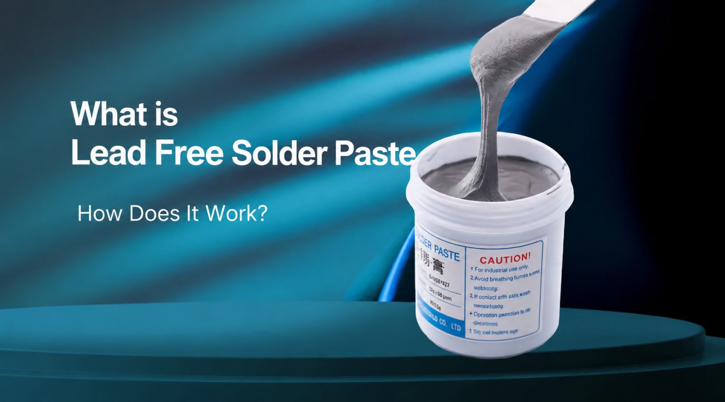
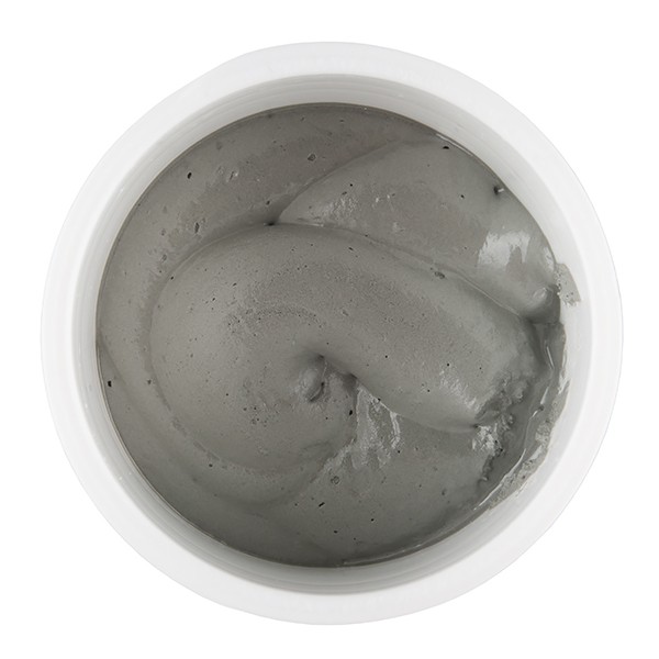
Solder paste is a thixotropic suspension of metal alloy powder in a flux vehicle fluid under squeegee pressure, stable once deposited. Removing lead forces a complete redesign of flux chemistry to handle higher temperatures and the oxidation behavior of tin-rich alloys.
How Lead-Free Solder Paste Is Formulated
The best lead-free solder paste is 88–90% metal alloy powder by weight, with 10–12% flux vehicle. Powder is classified into Types per IPC J-STD-005B. Choosing the wrong one for your finest feature causes aperture-release failures:
| Powder Type | Size Range (μm) | Typical Application |
|---|---|---|
| Type 3 | 25–45 | Standard SMT, >0.5 mm pitch |
| Type 4 | 20–38 | Fine pitch, 0.4 mm BGAs, 0201s |
| Type 5 | 15–25 | Ultra-fine pitch, 01005 chips |
| Type 6 | 5–15 | Jet printing, high-density specialty |
The flux vehicle handles oxide removal and ensures consistent squeegee flow, while surviving 240°C+ reflow without charring — a tougher brief than anything leaded-era flux chemistry had to meet.
SAC305 Solder Paste and Other Common Alloys
The search for reliable lead-free materials led to the tin-silver-copper (SAC) family. Specifically, sac305 solder paste (Sn96.5/Ag3.0/Cu0.5) became the global industry standard. It behaves as a near-eutectic alloy. It provides a reasonable melting range and excellent mechanical reliability.
However, specific industrial applications require alternative alloys:
- High-Silver Options (SAC387, SAC405): These contain 3.8% and 4.0% silver. Both are near-eutectic alloys with a narrow melting range right around 217–218°C. They deliver superior wetting and fatigue life but carry a higher silver cost.
- Silver-Free Alloys (SN100C): This Sn-Cu-Ni+Ge system melts at 227°C. It creates smooth, shiny joints. It completely eliminates the costly "silver tax" in high-volume consumer goods.
- Low-Temperature Alloys (Sn-Bi-Ag): Formulations like Sn42/Bi57/Ag1 melt at just 138°C. They protect ultra-sensitive components and enable safe step-soldering processes.
- Doped Alloys: Modern blends add trace amounts of bismuth (Bi) or nickel (Ni). These additives boost thermal cycling life and drop-shock durability.
Standards You Should Know
Authoritative manufacturing relies on international standards. Compliance ensures safety and reliability:
- RoHS — <0.1% lead by weight in homogeneous materials
- REACH — SVHC chemical disclosure for EU market entry
- IPC J-STD-006 — alloy classification and impurity limits
- IPC J-STD-005B — paste characterization: viscosity, slump, tack life
- IPC-7525C — Stencil Design – Benchmarks of Area and Aspect Ratio
Lead-Free Solder Paste vs. Leaded Solder Paste: Key Differences
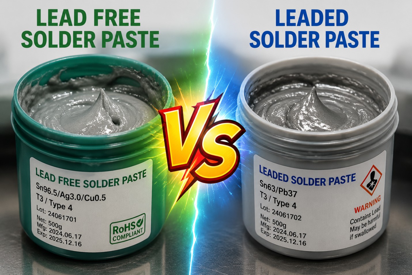
Switching from the old tin-lead (Sn63/Pb37) was not easy. Leaded solder was virtually the ideal material for assembling. It offered superb wetting, a low melting point, and highly ductile joints. Conversely, managing a leaded solder paste alternative requires strict control.
Composition and Material Cost
The economic impact of metal chemistry is substantial. Leaded material uses inexpensive tin and lead. Lead-free options rely heavily on precious silver. In the current commodity market, silver price volatility makes SAC305 roughly two to three times costlier than leaded equivalents. This cost penalty drives mass-production lines to adopt silver-free alloys like SN100C.
Melting Point, Wetting, and Joint Appearance
The traditional combination of Sn:Pb (63:37) has a dramatic 183°C melting temperature at the eutectic point. SAC305 melts higher, between 217°C and 220°C. This 34°C increase shrinks the process window. It leaves less room for error before components suffer thermal damage.
Lead-free alloys also exhibit high surface tension. This slows down wetting performance. While leaded alternatives wick up component leads effortlessly, lead-free variants flow sluggishly.
They often fail to spread to the absolute edge of pads on OSP or lead-free HASL finishes. The resulting joints look naturally dull and grainy. Technicians must be trained not to confuse this satin finish with a defective cold joint.
| Property | Leaded (Sn63/Pb37) | Lead-Free (SAC305) |
|---|---|---|
| Melting Point | 183°C (Eutectic) | 217–220°C (Near-Eutectic) |
| Surface Tension | Low (Excellent wetting) | High (Sluggish wetting) |
| Joint Finish | Highly shiny, smooth | Dull, grainy, satin-like |
| Tensile Strength | Moderate | Higher (But more brittle) |
| Residue Cleaning | Relatively easy | Harder (Baked by high heat) |
| Solderability | Highly forgiving | Sensitive to pad oxidation |
Printing and Process Behavior
Lead-free options display higher viscosity and unique shear behaviors. Their flux formulas are more aggressive to combat high-heat oxidation. Because lead-free materials do not spread significantly during reflow, the printed deposit must be exact. It stays precisely where it lands. This makes perfect gasketing between the PCB and the stencil mandatory to prevent fine-pitch shorts./p>
When You Can Still Use Leaded Solder Paste
Leaded options are not entirely gone. Where joint failure is catastrophic, there are critical exemptions:
- Aerospace and Defense: Pure tin and high-tin lead-free finishes can grow tin whiskers — conductive single-crystal filaments driven by compressive stress in the tin layer. In high-reliability vacuum and high-vibration environments, these whiskers can bridge adjacent leads and cause shorts. Adding even 3–5% lead suppresses whisker formation, which is why aerospace and defense remain exempt from RoHS for these applications.
- Medical Implants: Lead joints are used in life-critical hardware, such as pacemakers, and have been proven to be extremely ductile.
- High-Power Systems: For some power dies with higher melting points (those with >85% lead content), alternatives are being tested. Until then, these types of systems remain exempt.
- Legacy Repairs: Restoration of legacy non-RoHS equipment requires matching historical materials.
Here's a quick comparison of the two different types of solder paste.
| Property | Leaded (Sn63/Pb37) | Lead-Free (SAC305) |
|---|---|---|
| Melting Point | 183℃ (Eutectic) | 217-220℃ (Near-Eutectic) |
| Surface Tension | Low (Excellent wetting) | High (Sluggish wetting) |
| Joint Finish | Highly shiny, smooth | Dull, grainy, satin-like |
| Tensile Strength | Moderate | Higher (But more brittle) |
| Residue Cleaning | Relatively easy | Harder (Baked by high heat) |
| Solderability | Highly forgiving | Sensitive to pad oxidation |
Lead-Free Solder Paste Melting Point and Thermal Profile
The thermal reflow profile acts as your process recipe. With lead-free chemistry, the stakes are elevated. Reflow peaks sit dangerously close to the destruction point of standard PCB substrates and components.
Melting Points by Alloy
Every soldering alloy has its distinctive temperature characteristics required to obtain good soldering with quality results. The table below shows the precise lead-free solder paste melting point.
| Solder Alloy | Melting Point (°C) | Alloy Classification |
|---|---|---|
| Sn-Bi-Ag | ~138 °C | Low-Temperature Lead-Free |
| Sn-Pb37 | 183 °C | Traditional Leaded (Reference) |
| SAC387 | 217–218 °C | Eutectic Lead-Free |
| SAC305 | 217–220 °C | Near-Eutectic Lead-Free |
| SN100C | 227 °C | Silver-Free Lead-Free |
Thermal properties vary significantly across these distinct material groups. The composition of the liquidus and solidus lines is an important parameter for engineers to consider with special care to avoid defects in sensitive components in the reflow oven.
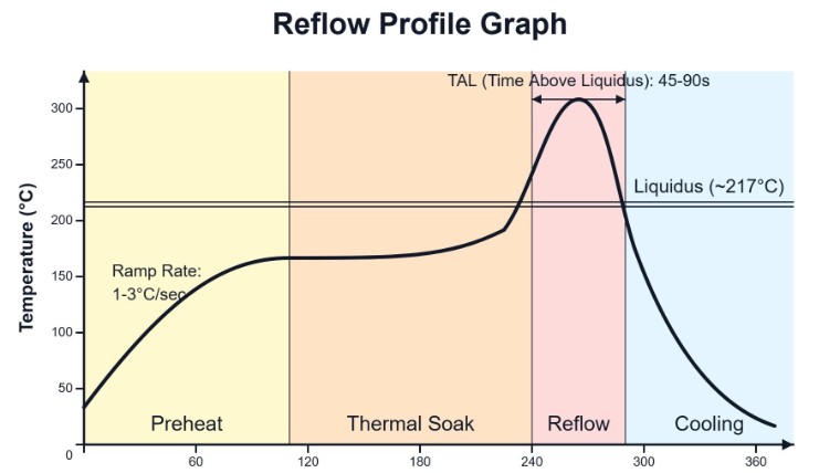
Building a Reflow Profile for Lead-Free Solder Paste
A dependable profile for SAC305 consists of four essential thermal zones:
Preheat Zone
A linear heating zone that takes the assembly from room temperature to 150°C. Avoid a ramp rate in excess of 1.5–3.0°C/s to prevent "thermal shock".
Soak Zone
Soak between 150°C–200°C for 60 to 120 seconds. This stage equalizes the temperature difference (ΔT) between small-sized passives and large-sized ICs.
Reflow Zone
Heat to a maximum of 235°C to 250°C. Maintain a critical Time Above Liquidus (TAL) of 45 to 90 seconds. This duration ensures the proper formation of the tin/copper intermetallic compound (IMC) layer.
Cooling Zone
Rapidly cool the board at a rate of 3–4°C/s. Fast cooling refines the grain boundaries, producing stronger joints.
Why a Higher Melting Point Matters Downstream
Bumping reflow peaks to 245°C strains the entire system. Substrates are at risk of delamination, warpage, and measling. Component buyers must ensure all parts carry a lead-free compatibility rating.
Legacy electrolytic capacitors and plastic connectors will deform at these temperatures. High heat also accelerates pad oxidation, demanding robust flux performance.
How to Choose the Best Lead-Free Solder Paste for Your Project
When choosing the paste, you'll need to take into account the design density, long-term operating conditions, and financial costs. Finding the best lead-free solder paste involves checking four core parameters.
Match the Alloy to the Application
-
Standard Prototyping:
Stick to SAC305. It features the largest operational dataset and global availability.
-
Mass Consumer Goods:
Deploy SN100C to reduce the cost of silver and retain high joint cosmetics.
-
Sensitive Flex-Rigid Work:
Low-Temperature Sn-Bi-Ag is designed for use with heat- and/or work-sensitive substrates.
-
Harsh Environments:
Use high-silver SAC Alloys or Doped Alloys for extreme mechanical and thermal stress and cycling conditions.
Choose the Right Powder Size (Type)
Match your powder sphere diameter to the tightest feature spacing on your PCB layout:
-
>0.5mm Pitch: Use Type 3 25-45m. It is highly economical.
-
0.4-0.5mm Pitch: Step up to Type 4 20-38m. This is the modern SMT baseline.
-
<0.4mm Pitch: Leverage Type 5 15-25m for micro-BGAs and fine components.
No-Clean vs Water-Soluble Flux
-
No-Clean (NC):
Eliminates expensive washing processes. The remaining residue is conductive and stable, but may cause problems with automated circuit testing.
-
Water-Soluble (WS):
Organic acid (highly aggressive) is soluble. An easy method of removing oxides, but the remaining residue is corrosive.
Shelf Life, Storage, and Working Life
Always store paste containers inside a dedicated refrigerator at 2°C to 10°C. This stops the active flux from attacking the metal spheres early. When pulling paste from cold storage, let it warm up naturally for 4 to 8 hours.
Never force-heat it. Open the tub only when it reaches room temperature. Otherwise, humidity will condense inside, causing severe voiding and solder balls. Limit on-stencil working life to 4–8 hours.
Applying Lead-Free Solder Paste: Why Your Solder Paste Stencil Is Critical
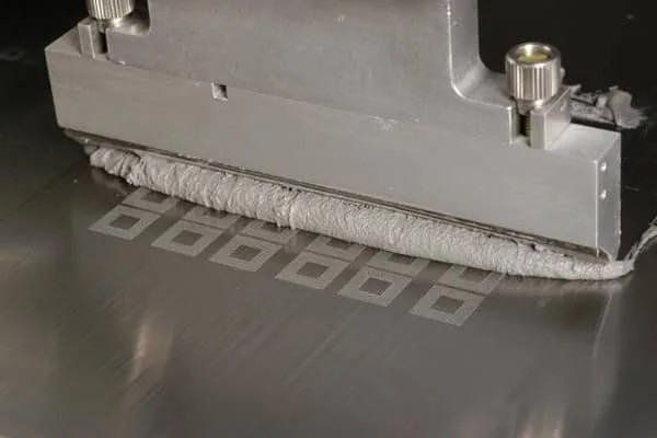
Because lead-free options flow sluggishly, your solder paste stencil determines your ultimate yield. It acts as the primary barrier against SMT printing defects.
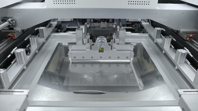
The Stencil's Role in the SMT Printing Process
The foil sets the X-Y boundaries and controls the Z-axis volume of your deposits. For fine-pitch designs, paste release becomes a mechanical challenge. If your aperture walls have rough surfaces, the paste stays stuck inside the slot rather than transferring cleanly to the circuit pad.
Aperture Design and Area Ratio for Lead-Free Paste
Two critical variables, Area Ratio and Aspect Ratio, should be calculated by engineers based on those defined in IPC-7525C formulas:
Key Formulas
Area Ratio = Aperture Base Area / Aperture Wall Area
Aspect Ratio = Aperture Width / Foil Thickness (L/W)
(Where L is length, W is width, and T is foil thickness)
For clean release, always target an Area Ratio ≥ 0.66 and an Aspect Ratio ≥ 1.5. If a tiny 0.4mm-pitch QFN pad falls below these limits, reduce your stencil thickness or request specialized wall treatments.
Stencil Thickness for Lead-Free Solder Paste
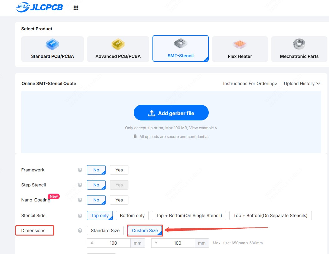
The total solder amount depends on the foil's thickness. JLCPCB offers standard choices including 0.10, 0.12, 0.15, 0.18, and 0.20 mm at no extra charge. They also provide special foils down to 0.03 mm for special applications:
- Standard Passives 0805+ Products: Use a 0.15mm foil.
- Superior Fine Pitch ICs 0.5mm: Shrink the size to 0.12mm foil.
- Ultra-Fine Components 0.4mm: Use a 0.10mm foil.
Stencil Material, Finish, and Coatings
The stainless steel is of high-grade 304 HTA for long-lasting tension stability.
-
Precision Laser Cutting:
Advanced facilities such as JLCPCB control 0.003mm aperture accuracy by means of an industrial laser cutting system.
-
Electropolishing:
A chemical process that removes any microscopic rough edges caused by the laser's cut.
-
Nano-Coating:
This premium hydrophobic treatment makes paste easy to shed. It drops your under-stencil wiping frequency from every 5 prints down to every 50 prints.
Step Stencils for Mixed-Volume Boards
Standard stencils feature a uniform thickness across the entire foil. This single-thickness approach fails when a circuit board combines ultra-fine-pitch components with massive, bulky connectors.
Fine-pitch pads need a thin foil to prevent bridging. Meanwhile, heavy power components require a thick foil to deposit sufficient solder volume. Step stencils resolve this mismatch by altering the foil thickness in targeted zones.
The Mechanics of Solder Volume and Paste Release
Foil thickness directly dictates theoretical solder volume: Volume = Aperture Area × Foil Thickness
The Area Ratio compares the aperture opening area to the total area of the aperture walls: Area Ratio = Area of Aperture Base / Area of Aperture Walls
For a clean paste release, this ratio must remain above 0.66. When you decrease foil thickness in a targeted zone, you reduce the surface area of the aperture walls — boosting the Area Ratio and enabling sticky solder paste to release cleanly onto tiny pads instead of clogging the stencil.
Squeegee Dynamics and Keep-Out Requirements
Varying foil thickness introduces physical, vertical steps on the squeegee side of the stencil. This transition modifies how the squeegee blade deposits paste.
As the rubber or metal squeegee passes over a step, it must deflect and adapt to the new height. If an aperture sits too close to a step edge, the squeegee cannot seal properly against the foil.
This lack of compliance causes two major defects:
Two major defects
- Paste Scooping: The blade digs too deeply, removing the required paste.
- Solder Skipping: The blade bridges over the area, leaving insufficient paste.
To prevent this, engineers must maintain strict keep-out zones around step transitions. A common industry rule is a clearance slope ratio of 20:1 to 30:1 relative to the step height, with up to 36:1 used as a conservative upper bound for sensitive fine-pitch designs. For example, a 1-mil (0.025 mm) change in foil thickness typically requires 20–30 mils (0.5–0.75 mm) of clearance between the step boundary and the nearest component aperture. This gap ensures full squeegee compliance and a proper gasket seal./p>
Primary Configurations: Step-Up vs. Step-Down
There are two primary ways to distribute volume across intricate layouts:
-
Step-Up Stencils:
These use a thin base foil (e.g., 4 mils) across the board to protect fine-pitch components. The manufacturer adds electroformed or welded thicker sections (e.g., 6 mils) around large connectors. This delivers the high solder volume needed for mechanical strength without flooding nearby micro-components.
-
Step-Down Stencils:
These utilize a thick base foil (e.g., 6 mils) for bulk components. Chemical milling or laser etching reduces the thickness (e.g., to 4 mils) near fine-pitch BGAs or QFNs. This limits paste volume, completely eliminating the risk of shorts and bridging.
Achieving this delicate balance is straightforward with the right manufacturing partner. JLCPCB supports custom step stencils, allowing you to optimize volume distribution across intricate, mixed-technology layouts.
Why Engineers Choose JLCPCB Stencils for Lead-Free Printing
JLCPCB supports over 6 million engineers globally by rendering advanced SMT tooling accessible:
- Instant Online Quoting: Skip the endless email back-and-forth. Simply upload your Gerber or DXF files to receive an immediate pricing quote.
- Rapid 12-Hour Turnaround: Keep your tight production schedules on track. Advanced production lines can complete your stencil build in as fast as 12 hours.
- Prototyping-Friendly Terms: Budget-conscious projects are welcome. Pricing starts at just $3 with a minimum order quantity of a single piece.
- Industrial-Grade Materials: Durability comes standard. Each stencil is crafted from premium 304 HTA stainless steel and mounted to high-tension aluminum frames.
- Micro-Level Accuracy: Avoid alignment issues on fine-pitch components. High-end laser systems cut apertures with a tight precision of 0.003mm.
- Advanced Custom Upgrades: Protect your yields on complex layouts. You can easily add optional electropolishing, nano-coating, ultrasonic-resistant adhesives, or step stencils.
-
Symptoms: Pads show dry spots or severely shortened volumes.
-
Causes: Paste crusting blocks the openings, or the Area Ratio is below 0.66.
-
Prevention: Follow the 5-ball rule. Apply electropolished or nano-coated stencils, and replace old paste every 4 hours.
-
Symptoms: Unwanted solder bridges cause short circuits, or tiny metal spheres scatter across the soldermask.
-
Causes: Excess print volume or poor gasketing lets paste bleed underneath the foil.
-
Prevention: Shrink aperture windows by 5% to 10% relative to pad size. Maintain solid stencil tension and reduce squeegee pressure.
-
Symptoms: Large internal gas bubbles are visible on X-ray.
-
Causes: Volatile flux gets trapped beneath large, solid ground planes during reflow.
-
Prevention: Replace solid stencil openings with a window-pane cross-grid pattern. This breaks up the paste mass and opens escape vents for gas.
-
Symptoms: Small passives stand upright on one terminal, or joints display deep cracks.
-
Causes: Uneven heating or fast ramp rates cause one pad to melt before the other.
-
Prevention: Extend your thermal soak duration to 90 seconds. Keep your apertures perfectly symmetrical and verify a minimum TAL of 60 seconds.
Choose from Framed/Frameless, Electropolishing, Nano-coating, Step-Stencils, SMD Glue Stencil and more. Starting at $3. No MOQ. 12-Hour production.
Get $11 Coupon Now >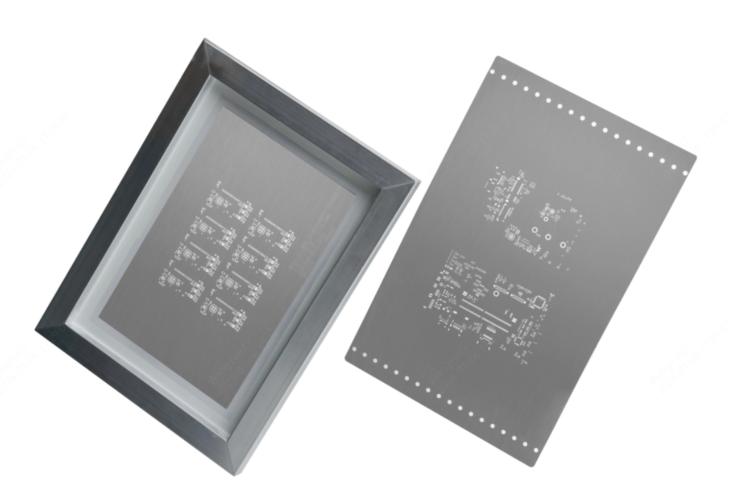
Common Lead-Free Solder Paste Defects (and How to Prevent Them)
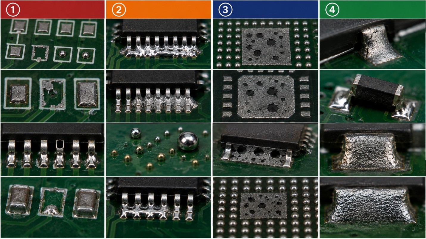
Lead-based processes are less sensitive to printing anomalies. Resolving these defects requires balancing stencil attributes and paste handling.
1Insufficient Solder Deposits and Skips
2Bridging, Smearing, and Solder Balling
3Voiding Under BGA and QFN Thermal Pads
4Cold Joints, Tombstoning, and Grainy Joints
FAQs: Lead-Free Solder Paste Printing & Reflow
Why are my lead-free joints dull and grey?
Normal. SAC305 and SN100C naturally form a satin crystalline finish. A dull joint isn't a cold joint. Look for non-wetting at pad edges or cracks in the fillet, not color, as failure indicators.
What's the difference between ROL0 and ROL1 flux?
ROL0 is halide-free (<0.05%), the safest choice for high-reliability no-clean applications. ROL1 allows up to 0.5% halides for better wetting on oxidized pads. At lead-free temperatures, that activator difference can visibly affect yield on difficult pad finishes.
Is SAC305 compatible with leaded solder?
Mixed joints have unpredictable melting points and an increased risk of early fatigue failure. More critically, any lead contamination renders the board non-RoHS-compliant — legally unmarketable in the EU and most regulated markets.
What is the five-ball rule for stencil apertures?
Minimum aperture ≥ 5× largest powder particle diameter. Type 4 powder (max 38 μm) needs a minimum aperture of 190 μm. Otherwise, paste bridges across the opening instead of transferring to the pad.
How do bottom-side components stay attached during a second reflow pass?
They hold on through pure surface tension. When a double-sided board is flipped for its second pass, the bottom-side solder actually remelts completely into a liquid state. However, the high surface tension of lead-free alloys acts like an invisible clamp. It pulls the component leads upward, easily counteracting gravity for lightweight parts like resistors and small ICs.
Conclusion: Mastering Lead-Free Solder Paste Printing
Managing lead-free assembly requires a strict discipline rooted in materials science. Success depends on selecting your materials wisely — balancing the field-proven reliability of SAC305 with the cost savings of SN100C.
While tuning your thermal reflow profile protects sensitive components, printing precision remains your strongest tool. A high-quality stencil designed to strict IPC area ratios eliminates most assembly defects before the board ever reaches the oven.
By working with manufacturing partners like JLCPCB, you gain access to industrial laser-cut stencils featuring 0.003 mm accuracy and 12-hour turnaround times. This precision lets you overcome lead-free processing challenges and deliver robust electronics to the global market.
Keep Learning
The Complete Stencil Guide for Lead-Free Solder Paste Printing
Key Takeaways SAC305 is the global standard: Sn96.5/Ag3.0/Cu0.5 offers a near-eutectic melting range of 217–220°C, excellent mechanical reliability, and broad industry acceptance. SN100C (Sn-Cu-Ni+Ge) is the leading silver-free alternative for high-volume cost reduction. 34°C higher melting point shrinks process window: Lead-free alloys melt ~34°C higher than Sn63/Pb37, requiring tight reflow profiles with peak temperatures of 235–250°C and TAL of 45–90 seconds. Paste storage is non-negotiable: Store ......
SMD Assembly vs THT Assembly: A Practical Guide
Every PCB design eventually faces the same fork: should this part be SMD or THT, and what does that choice actually mean for the manufacturing line? The distinction between SMD and THT assembly extends far beyond component selection. It requires two completely separate manufacturing toolchains and introduces entirely distinct defect modes. For mixed-technology layouts, a critical intermediate step is the bottom-side adhesive process. This stage involves dispensing precise dots of thermosetting epoxy t......