
PCB Troubleshooting : How to Diagnose Issues and Prevent Failures Through Professional Manufacturing
14 min
- Common PCB Problems Engineers Face
- Step-by-Step PCB Troubleshooting Process
- Diagnosing Root Causes: Beyond the Symptoms
- Preventing PCB Problems at the Manufacturing Stage
- Common PCB Failures and Professional Prevention
- When to Troubleshoot vs. When to Redesign
- How JLCPCB Helps Reduce PCB Troubleshooting
- PCB Troubleshooting Checklist
- Frequently Asked Questions (FAQ)
Modern PCBs can pass bench tests yet still fail later due to subtle defects. Faulty PCBs are unavoidable from time to time, which makes knowing troubleshooting techniques useful. Often, human error in manufacturing can cause problems from a slightly shifted trace to a tiny solder void. Identifying and fixing these issues early saves money and time because defective PCBs result in increased rework costs and delayed production. If a defect is caught in the early stages of prototyping, it can save thousands for a fab. In practice, troubleshooting is a systematic process of symptom analysis and targeted tests. The key insight is to combine careful diagnosis with preventive design. Best to catch errors either in layout or assembly before they become production headaches.
Why Issues Emerge Post-Testing or in Production
Some defects are latent and thus, the errors may come out after the first testing or even in the field. Minor manufacturing defects are unlikely to cause instant death of the board, but will lead to intermittent failures in the product when stressed. Other design oversights, like the omission of decoupling capacitors or inadequate voltage margins, can similarly be revealed only by real loads. Failures that were not detected during lab tests can also be caused by environmental factors and rough treatment. Concisely, a PCB can exit the factory in a clean state. However, there may be latent weaknesses that will show up after the board has been powered, heated, or put under actual operational conditions.
Costs of Troubleshooting: Reworks, Delays, and Risks
The financial and schedule impact of PCB troubleshooting can be steep. Every defective board that must be reworked or scrapped wastes materials and labor. For example, even a 5% defect rate on a 10,000‑board run can cost thousands of dollars in wasted boards and repair time. Repairing boards ties up technicians and delays deliveries, a serious risk if time‑to‑market is critical. Hidden costs include disrupted supply chains and even loss of customer trust if failures slip out. Put simply, a single bad solder joint can cascade into a major bottleneck. Finding and fixing errors early lowers the possibility of expensive changes and prevents whole batches from stalling factory lines.
Key Insight: Diagnosis Combined with Prevention
Troubleshooting is like detective work and analysis of engineering. The most effective fixes are those that occur when you recognize the symptom and narrow down to the cause of the symptom. Practically, that would imply the re-check of design specifications and production procedures, even prior to the shipment of the boards. According to studies conducted by industry players, poor PCB quality has the potential to cost you 10-20 percent of revenue in case you allow it to go to waste. On the other hand, design with DFM tools and adherence to IPC rules gives you the opportunity to identify a significant number of issues early on. The majority of PCB failures are a result of human mistakes during the manufacturing process, however, with the ability to identify those errors and eliminate them, you can in fact save time and save a fortune.
Common PCB Problems Engineers Face
Power and Signal Issues Like Instability or Noise
Power and signal integrity problems are frequent culprits. Unstable or noisy power rails can cause erratic operation. Inadequate decoupling capacitors or broken ground planes let voltage droop and noise ripple through logic. Decoupling capacitors must be placed right at each IC’s supply pins to stabilize fast transients. Without good decoupling, large digital ICs draw surges of current that show up as voltage glitches or brown-outs.
On the signal side, high-speed lines suffer from crosstalk and EMI. Parallel traces running too close together couple noise between nets, corrupting data. Fortunately, design rules can minimize this by keeping sensitive lines over a solid ground plane. Impedance mismatches cause reflections and high-frequency ringing. In summary, power/signal issues manifest as random resets, data errors, or reduced noise margins. Engineers should check the supply voltage levels and stability, ground plane continuity, and critical signal waveforms.
Soldering Defects, Component Failures, and Thermal Problems
In that way, a significant number of PCB failures are experienced at the assembly stage. In case reflow or wave soldering fails, to reach the correct temperature or timing, cold joints, solder bridges, tombstoned parts, or voids occur. These ones are visible with dull or grainy solder fillets and components that appear tilted or tombstoned on one side. The good news? Most of such bugs can be avoided by using the IPC-A-610 workmanship standards. Even automated inspection such as AOI and X-ray is already used to pick up a ton of solder defects before the boards even ship.
Overheating and component malfunctions are also quite prevalent. Burn marks or bulging on the board surface is the characteristic of overheated ICs or capacitors. Fractures inside leads and packages can occur due to high temperature. Actually, one of the largest causes of failure of the circuit boards is overheating. Burnt parts, broken substrates, or sensors that drift out of spec will be spotted by engineers when under stress.
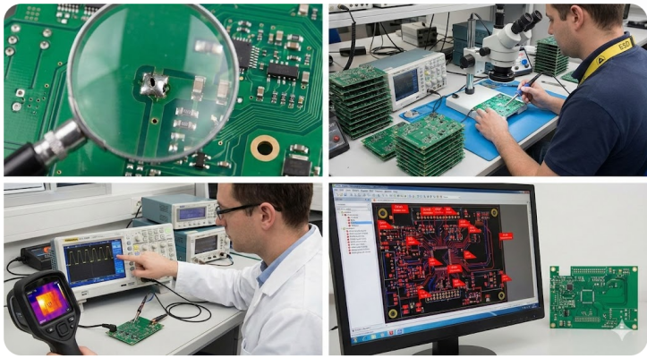
Step-by-Step PCB Troubleshooting Process
Visual Inspection for Damage and Misalignment
You start with the visual inspection of the board - just a flick of the eye in good light to identify the obvious damage. Look at broken parts, floating pads, or ugly solder bridges. Burn marks normally indicate something that overheated. Check bloated or broken electrolyc caps, deteriorated ICs, lost or misaligned bits and any smudged or bridged solder. Cold joints are usually dull or grainy. Ensure that the polarization of each part is corresponding to the silkscreen and schematic. In case you can not see something with the naked eye, use a microscope to identify hairline cracks or solder voids. Notice to the copper by tilting the board. And scribble/silkscreen typo, sometimes, suggests a mismatch.
Electrical and Functional Testing Methods
Once the visual material is done, you are now ready to boot it up or spin up a simulation. Begin with a multimeter to test the supply rails - measure those voltages, drop to continuity mode and ensure that the grounds are only contacting what they are supposed to, and that there is no accidental short between the power nets. All the connector pins and nets you are hoping will be continuous should not be on all the other pins. The next step is to check probe signals using an oscilloscope or logic analyzer- verify that waveforms at important test points are correct as per the datasheet. In the case of clocks, buses, and analog, an oscilloscope (or any other waveform-capture equipment) will reveal you edges and shape. A thermal camera has the ability to detect hot spots on the board. You should use a soldering iron or rework station when you strike a bad joint. And in case you have to check off-board LCR meter to read passive values.
Diagnosing Root Causes: Beyond the Symptoms
Design and Manufacturing-Related Issues
A symptom often has a deeper root. One must ask, is it a layout/design flaw or a build defect? Common design culprits include incorrect footprints, insufficient clearance, or wrong layer stack. Violating the manufacturer’s DFM rules, such as using trace widths below the fab minimum or spacing that is too tight and invites yield issues. Always cross-check the PCB against design rules and component datasheets (see JLCPCB’s design guidelines).
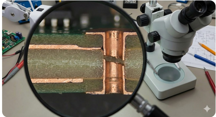
Manufacturing faults can hide even in a perfect design. For instance, incomplete plating or lamination can lead to open vias or even layer separation. Misalignment in layer registration might shorten adjacent planes. Contamination during fabrication can cause intermittent shorts or solderability issues.
Handling and Assembly Problems Like ESD or Stress
Hence, in addition to chips and solder, how you handle a board may actually make it fail. ESD during assembly or testing can silently kill ICs resulting in bizarre glitches in the future. Traces can be snapped off by mechanical stress or the plated through holes can be worn out. One of the classic indications of mechanical damage is a board that is functional until you bend it or bang it; at which point it loses its head. BGAs can popcorning under the influence of moisture taking up, resulting in the peeling off of layers or the pitting of solder balls when the board is heated.
Ensure that you use ESD-safe mats and tools, adhere to thermal soak profiles such that you do not shock the board with moisture, and ensure that the board is well supported when assembling it. Tune the conditions of your tests when debugging: a component that was stuck may start working after you cool or clamp it, and the guilty party may be mechanical.
Preventing PCB Problems at the Manufacturing Stage
DFM Optimization and Process Controls
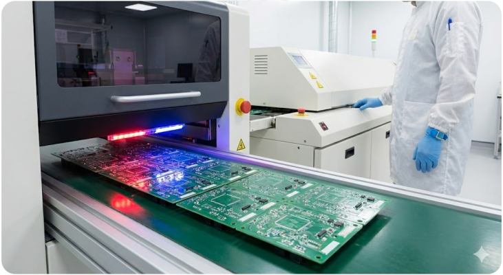
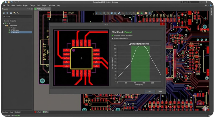
A robust design for manufacturability (DFM) is the best preventive measure. During layout, engineers should follow IPC and fab-specific rules: set proper trace/space, pad size, via dimensions, and consider thermal reliefs. Applying DFM guidelines avoids common fab defects. Tools like JLCPCB’s free online DFM analyzer can automatically flag violations before fabrication. Rule-checkers should also enforce correct solder mask clearances and component spacing (for pick-and-place). At the fab, process controls ensure those DFM choices become reality. Every board typically goes through AOI and X-ray inspection to catch assembly defects. Reflow ovens follow tightly controlled profiles to achieve reliable solder joints.
Material Selection and Cleanliness Standards
The choice of materials and their cleanliness impact on reliability tremendously. Proven PCB substrates with the correct glass transition (Tg) and CTE values are used to ensure that the board can withstand all those thermal cycles and high frequency signals. An illustration is that JLCPCB selects resins that exceed the UL94 V 0 flammability standard. Simply, you select the PCB finish that suits your project.
In the production and assembly, it is important to maintain cleanliness. Flux residue, dust or metal particles may absorb moisture or spit out under bias, giving rise to leakage or shorts. The IPC standards are quite rigid and provide that you must clean following the process of soldering: post-reflow PCBs must be devoid of any form of conductive residues. Once you have to add the final coating or conformal layer, you must do it without trapping any air or contaminants. To pull out moisture, solid manufacturers do pre-assembly bake-outs to maintain their cleanrooms spotless for stencils and reflow.
Common PCB Failures and Professional Prevention
Solder Defects Prevented by DFM and Profiles
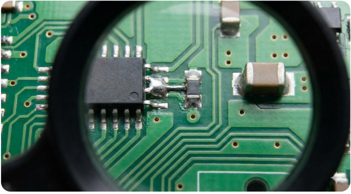
Common pain points in the everyday struggle in the laboratory are typical heavy-metal headaches such as solder bridges, insufficient solder, and tombstoning. DFM-aware footprints and right reflow profile are the initial step in the cure. It is important to have pads of the necessary size, apertures of the paste aligning correctly, a uniform distribution of solder, and so on. Through the addition of thermal chokes or balancing resistors to either side of a pad, fundamentally, components are prevented from turning over. IPC-A-610 defines it as follows: the solder joints must be concave, smooth and free of any voids or bridges. Practically, that would be heating and immersing the board in such a way that the solder fully wets the pads. Engineers must maintain a tight contact with fabricators to pin the temperature profiles of whatever mix we are using.
At the assembly stage, we defend with a quick hand check and AOI scan. One trick is simply to push component pads a bit out of center on the pads so that the solder wick can be reflowed flat. Preemptively, the design reviews should check thermal pads and ground vias between the components to wipe out tombstoning potential and ensure the solder fills all the spots.
Delamination and Via Issues Prevented by Qualification
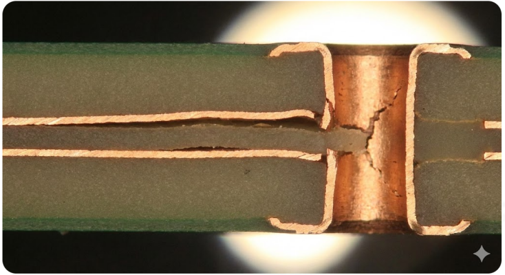
Layer separation and via/copper issues often stem from material or process faults. Delamination can occur if moisture-laden boards are heated too rapidly or if the resin cure is incomplete. Using qualified materials and validated lamination processes prevents this. Via failures are avoided by sticking to aspect ratio rules and design guidelines. Sufficient annular ring around vias and holes is critical. JLCPCB’s DFM tool explicitly flags if the ring is too thin. In design, try to keep via aspect ratio within recommended limits and use via-in-pad plating where needed. In summary, preventing delamination and via cracks is largely a matter of using certified board materials and following IPC qualification processes.
When to Troubleshoot vs. When to Redesign
One of the major decisions is the fixes vs redesign. The notion of quick fixes is rational in the case of minor board runs or prototypes. A technician can usually fix one net at the lab bench, or even a component, when it is incorrect or open. The causes of redesign triggers are multiple board failures, frequent low yields, or any defect that does not meet end-use requirements. Likewise, when assembly indicates that tombstoning occurs on a high percentage of joints, the PCB footprint or reflow profile must be re-worked, and not repaired over and over again.
Practically, it is guided by the rule of thumb: in case repair needs more than two site-specific interventions, redesign the PCB. Huge volume production implies that it has to be reliable by design; failure of at least one in thousands may not be tolerated. The red lines of mass production could be specified by the IPC class of the product.
How JLCPCB Helps Reduce PCB Troubleshooting
Free DFM Feedback and Inspections
JLCPCB provides tools to catch issues before manufacturing. Designers can use JLCPCB’s free online DFM checker or consult its guidelines to verify that trace widths, drill sizes, spacing, and annular rings meet the fab’s limits. The DFM tool instantly finds typical design flaws including component placement concerns, trace width violations, and clearance issues. This automated review means many potential failures are flagged early, avoiding respins.
AOI checks will catch a half-masked pad or insufficient solder volume. JLCPCB also performs flying-probe or X-ray tests as needed to verify nets and internal connections. In essence, their pre-production inspection is a safety net: known trouble spots like annular ring clearances are checked against the chosen stack-up, and assembly is checked by standards.
PCB Troubleshooting Checklist
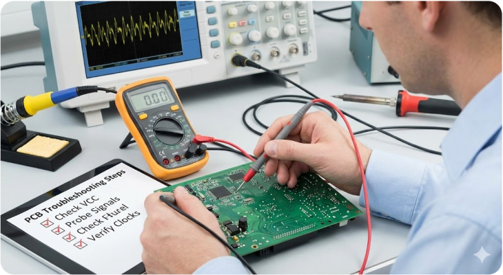
With a multimeter, confirm that each supply voltage is at its nominal level before powering sensitive parts. Check for shorts by measuring resistance between VCC and GND. If a rail reads 0 V, investigate possible short circuits or missing components. Use the DMM’s continuity mode on crucial nets. Ensure grounds are common and that nets which should be isolated indeed have no shorts.

Once powered, measure actual voltages at regulators, references, and ADC/DAC pins. Unexpected drops or noise here indicate decoupling issues. Use an oscilloscope to probe clocks, data buses, and analog signals. Compare waveforms against expected reference shapes. For digital signals, verify correct logic levels. For high-speed edges, look for ringing or reflections. Check decoupling caps with an LCR meter if in doubt. Faulty caps often have much higher impedance or outright open failure.

Frequently Asked Questions (FAQ)
Q: What tools are essential for PCB troubleshooting?
A: A digital multimeter (DMM) is fundamental for checking continuity and voltages. An oscilloscope is crucial for examining signal waveforms and noise. Others include an LCR meter, a thermal camera, and a logic analyzer for digital buses.
Q: How can I quickly locate a short or broken trace?
A: First, with the board powered off, use the DMM in continuity mode to find unexpected connections. An open circuit on a net that should be continuous signals a break. Power on briefly and measure each rail voltage and a rail stuck at 0 V often means a short.
Q: What design practices help avoid these issues?
A: Follow strict DFM rules and IPC guidelines. Always include decoupling capacitors close to IC power pins and maintain adequate spacing on high-speed traces to prevent crosstalk.
Q: How does JLCPCB’s DFM tool and inspection help me?
A: JLCPCB offers a free online DFM checker that analyzes your Gerber files before fabrication. It instantly flags design errors.
Q: What IPC standards should I follow for solder quality?
A: The IPC-A-610 standard is the benchmark for solder joint acceptability. It specifies criteria for SMT and through-hole joints.
Keep Learning
Etched FPC: Manufacturing Process, Advantages, Applications, and Selection Guide
Ever noticed that thin, amber-coloured ribbon running between the boards in a smartphone camera module or a notebook's lid? That ribbon is almost surely an etched FPC, a flexible printed circuit that's created by chemically removing the unwanted copper to create a precise conductive pattern. It's one of the workhorses of modern electronics, and most people are unaware of the amount of engineering that goes into it. There are more than one flavor of flexible circuit, and the method of manufacture affec......
The Critical Role of Copper Peel Strength in Durable PCB Performance
Key Takeaways Standard Test: Measured via the IPC-TM-650 90° pull test in N/mm. Core Function: Prevents pad lifting and delamination under thermal stress and CTE mismatch. Foil Types: ED foil provides higher adhesion; RA foil yields lower signal loss. Material Benchmarks: Standard FR4 averages 1.0–1.4 N/mm, while High-Tg FR4 achieves 1.2–1.6 N/mm. Design Tips: Add teardrops, eliminate unsupported copper slivers, and perform DFM checks. Ever wonder what's making the copper stay put on your circuit boar......
How Modular PCB Design Simplifies Complex Electronics Projects
Key Takeaway Modular PCB design simplifies complex electronics by breaking boards into independent, reusable functional blocks with clear interfaces. It boosts reusability, speeds up debugging, enhances team collaboration, and reduces errors.Shift from flat to modular design for faster development and more scalable, reliable PCBs. Ever seen a 400+ component schematic and got your head scrambled before even beginning routing? You are not alone. With the ever-increasing density of electronics combined w......
Your Ultimate Guide to PCB Rulers
In the world of PCB design and manufacturing, having the right tools is crucial for achieving accuracy and precision. One such tool that has gained popularity among professionals and hobbyists is the PCB ruler. This specialized measuring tool is designed to provide accurate measurements, reference information, and component footprints, assisting designers, engineers, technicians, and assemblers in various stages of PCB development. In this guide, we'll explore what a PCB ruler is, the features and mea......
Understanding the Materials Used in PCBs: Selection, Types, and Importance
Key Takeaways FR-4 is the go-to material for most cost-effective and reliable PCBs. Use Rogers for high-frequency and RF applications to reduce signal loss. Higher copper weight (2oz) improves current and heat handling. Choose High-Tg substrates for better thermal stability in multilayer boards. Green LPI soldermask offers the best balance of performance and inspection. Printed circuit boards (PCBs) are an essential component of modern electronics. These boards connect and support electronic component......
How to Select Tg of PCB ?
What is the Tg of PCB? In PCB manufacturing, "Tg" stands for Glass Transition Temperature. It is the temperature at which the PCB substrate material transitions from a rigid, glassy state to a soft, rubbery state. PCBs are flame-retardant (UL94 V-0) and do not burn easily; instead, they soften above Tg. The Critical Correlation Between Tg and Z-Axis CTE (Coefficient of Thermal Expansion) When the temperature exceeds the Tg point, the PCB substrate material (such as standard FR-4) undergoes a physical ......